CN100429509C - FET type sensor - Google Patents
FET type sensorDownload PDFInfo
- Publication number
- CN100429509C CN100429509CCNB028225392ACN02822539ACN100429509CCN 100429509 CCN100429509 CCN 100429509CCN B028225392 ACNB028225392 ACN B028225392ACN 02822539 ACN02822539 ACN 02822539ACN 100429509 CCN100429509 CCN 100429509C
- Authority
- CN
- China
- Prior art keywords
- input
- sensor
- substrate
- potential
- fet
- Prior art date
- Legal status (The legal status is an assumption and is not a legal conclusion. Google has not performed a legal analysis and makes no representation as to the accuracy of the status listed.)
- Expired - Lifetime
Links
Images


Classifications
- G—PHYSICS
- G01—MEASURING; TESTING
- G01N—INVESTIGATING OR ANALYSING MATERIALS BY DETERMINING THEIR CHEMICAL OR PHYSICAL PROPERTIES
- G01N27/00—Investigating or analysing materials by the use of electric, electrochemical, or magnetic means
- G01N27/26—Investigating or analysing materials by the use of electric, electrochemical, or magnetic means by investigating electrochemical variables; by using electrolysis or electrophoresis
- G01N27/403—Cells and electrode assemblies
- G01N27/414—Ion-sensitive or chemical field-effect transistors, i.e. ISFETS or CHEMFETS
- G01N27/4145—Ion-sensitive or chemical field-effect transistors, i.e. ISFETS or CHEMFETS specially adapted for biomolecules, e.g. gate electrode with immobilised receptors
Landscapes
- Health & Medical Sciences (AREA)
- Life Sciences & Earth Sciences (AREA)
- Chemical & Material Sciences (AREA)
- Molecular Biology (AREA)
- Physics & Mathematics (AREA)
- Analytical Chemistry (AREA)
- General Health & Medical Sciences (AREA)
- Engineering & Computer Science (AREA)
- Chemical Kinetics & Catalysis (AREA)
- Electrochemistry (AREA)
- Spectroscopy & Molecular Physics (AREA)
- Biochemistry (AREA)
- Microelectronics & Electronic Packaging (AREA)
- General Physics & Mathematics (AREA)
- Immunology (AREA)
- Pathology (AREA)
- Investigating Or Analyzing Materials By The Use Of Electric Means (AREA)
- Apparatus Associated With Microorganisms And Enzymes (AREA)
- Measuring Or Testing Involving Enzymes Or Micro-Organisms (AREA)
- Semiconductor Integrated Circuits (AREA)
Abstract
Translated fromChinese
Description
Translated fromChinese技术领域technical field
本发明涉及在MOS场效应晶体管(FET)的栅极绝缘膜上,形成感应离子的传感部,检测出基于该传感部表面电位变化的沟道电位电平变化量,来检测离子浓度的FET型传感器构造和利用此传感器构造的离子浓度检测方法和碱基序列检测方法。The present invention relates to forming a sensor portion for sensing ions on a gate insulating film of a MOS field effect transistor (FET), and detecting the amount of change in channel potential level based on a change in surface potential of the sensor portion to detect ion concentration. A FET type sensor structure and an ion concentration detection method and a base sequence detection method using the sensor structure.
背景技术Background technique
至今为止,作为利用集成电路技术的化学传感器,开发出利用FET原理的种种传感器。该FET型传感器是检测电化学电位变化的传感器,作为一例,叫做检测氢离子浓度的离子敏感FET(ISFET)。Various sensors utilizing the FET principle have been developed so far as chemical sensors utilizing integrated circuit technology. This FET-type sensor is a sensor that detects a change in electrochemical potential, and is called, for example, an ion-sensitive FET (ISFET) that detects a hydrogen ion concentration.
ISFET是在MOS FET的栅极绝缘膜上,形成感应离子的传感部的ISFET,把该ISFET浸在水溶液,检测出基于传感部电位变化的沟道电导的变化量,来求出水溶液中的氢离子浓度的构成。ISFET is an ISFET that forms a sensing part for sensing ions on the gate insulating film of the MOS FET. The ISFET is immersed in an aqueous solution to detect the change in channel conductance based on the change in the potential of the sensing part to obtain the value in the aqueous solution. The composition of the hydrogen ion concentration.
可是,ISFET存在:灵敏度低(能斯脱公式来求出的理论最大灵敏度为59mV/pH)、随时间的输出不够稳定、不能高精度地检测离子浓度等的问题。另一方面,在生化学测定领域中,只要能够提高ISFET的灵敏度,有希望:检测出低聚核苷酸的杂交(核酸杂种分子形成)发生的有无,从而,用于确定检体的碱基序列等。However, ISFETs have problems such as low sensitivity (theoretical maximum sensitivity obtained by the Nernst formula is 59mV/pH), insufficient stability of output over time, and inability to detect ion concentration with high precision. On the other hand, in the field of biochemical measurement, as long as the sensitivity of the ISFET can be improved, it is expected to detect the presence or absence of hybridization (nucleic acid hybrid molecule formation) of oligonucleotides, thereby determining the base of the sample. base sequence etc.
所谓杂交分析是指:准备与鉴别、检测和应分离的核酸(靶核酸)互补的单链核酸(探针),检测出试料的单链核酸是否与探针杂交,或测定出杂交的双链核酸的量的分析。The so-called hybridization analysis refers to: preparing a single-stranded nucleic acid (probe) complementary to the nucleic acid (target nucleic acid) to be identified, detected and separated, detecting whether the single-stranded nucleic acid of the test sample hybridizes with the probe, or measuring the double-stranded nucleic acid of the hybridization. Analysis of the amount of strand nucleic acid.
在该杂交分析上,应用凝胶电泳,作为研究核酸的碱基序列的方法,有萨瑟恩印迹法。在萨瑟恩印迹法中,首先,将规定长度的双链DNA片段进行凝胶电泳,把凝胶浸在碱性液体里,将利用电泳分离的双链,以保持带(band)的状态下,变为一条链。把该转移到DNA结合用的片材上。然后,将上述的片材浸在杂交形成液里,加上具有辐射能的探针,加温而杂交。由此,判断哪一个带和哪一个探针结合,由此,可以检测出对探针具有互补性的碱基序列的带。可是,该方法存在:处理繁杂、消耗时间和需要成本高的本质性的问题。从而,如上所述,探索出提高ISFET的灵敏度并应用在杂交分析等的生化学测定的方法是当务之急。In this hybridization analysis, gel electrophoresis is applied, and as a method for studying the base sequence of nucleic acid, there is a Southern blotting method. In the Southern blotting method, first, gel electrophoresis is performed on a double-stranded DNA fragment of a specified length, the gel is immersed in an alkaline liquid, and the double-strands separated by electrophoresis are kept in a band state. , becomes a chain. Transfer this to a DNA binding sheet. Then, the above-mentioned sheet is immersed in a hybridization solution, and probes with radiant energy are added, heated and hybridized. In this way, it is judged which band binds to which probe, whereby a band having a base sequence complementary to the probe can be detected. However, this method has the essential problems of complicated processing, time-consuming and high cost. Therefore, as described above, it is urgent to find a method for improving the sensitivity of ISFETs and applying them to biochemical measurements such as hybridization analysis.
发明内容Contents of the invention
本发明是鉴于这样的情况而进行的,其目的在于提供:离子型传感器构造和利用此传感器构造的离子浓度检测方法;其原理是:将基于ISFET传感部的表面电位变化的传感部正下方的势井深度的变化,作为漏极电荷来反复转送,其电荷应该积累在漏极上的构成,可以可靠地检测出传感部的表面电位的微量变化,从而可以高灵敏度地检测出离子浓度的变化。The present invention has been made in view of such circumstances, and its object is to provide: an ion-type sensor structure and an ion concentration detection method using the sensor structure; The change in the depth of the potential well below is repeatedly transferred as the drain charge, and the charge should be accumulated on the drain, so that a slight change in the surface potential of the sensing part can be reliably detected, and ions can be detected with high sensitivity. change in concentration.
如上所述,从源极向漏极转送n次而积累电荷时,漏极电位的变化量变为n倍而噪音为随机的值,只增加√n倍,因此,S/N之比变为n/√n=√n倍,而相应地提高灵敏度。由此,即使是基于传感部的表面电位变化的其正下方的势井深度的变化为微量,对其进行累积而可靠地检测出,从而可以高灵敏度地检测出离子浓度的变化。As mentioned above, when charge is transferred from the source to the drain n times to accumulate charge, the amount of change in the drain potential becomes n times and the noise is a random value, which only increases by √n times. Therefore, the S/N ratio becomes n /√n=√n times, and correspondingly improve the sensitivity. Thereby, even if the change in the depth of the well directly below the surface potential of the sensor part is slightly changed, it is accumulated and reliably detected, and a change in ion concentration can be detected with high sensitivity.
对上述的电荷积累原理的ISFET的基本构造,在以前,本发明人等已经发明,于平成12年9月27日,以「累积型化学·物理现象检测装置」的名称,提出申请(特愿2000-293669号)。该申请中公开的构造,是在上述的MOSFET的栅极绝缘膜上的栅极分割为两个、在其分割间隔上、插入离子感应膜(传感部)的构造的ISFET中,组合复位漏极电位的复位·晶体管的构造。The basic structure of the above-mentioned ISFET based on the principle of charge accumulation has been invented by the present inventors before, and an application was filed on September 27, 2012 under the title of "accumulation type chemical and physical phenomenon detection device" (patent request 2000-293669). The structure disclosed in this application is to combine a reset drain in an ISFET having a structure in which the gate on the gate insulating film of the above-mentioned MOSFET is divided into two, and an ion-sensitive film (sensing part) is inserted at the division interval. Potential reset and transistor structure.
因此,本发明的一个目的在于提供:在ISFET传感部上,通过固定与检体反应或结合的物质或固定检体的反应催化剂的物质,而正确地检测出基于所述反应或结合的离子浓度的变化,可以正确地检测出试料中的检体的有无或含量的FET型传感器和离子浓度检测方法。Therefore, an object of the present invention is to provide: on the ISFET sensor part, by immobilizing a substance that reacts or binds to a sample or a substance that immobilizes a reaction catalyst of the sample, and accurately detects ions based on the reaction or binding. A FET-type sensor and ion concentration detection method that can accurately detect the presence or absence or content of a sample in a sample due to changes in concentration.
并且,本发明的另一个目的在于提供:在ISFET传感部上,通过对与靶核酸互补的单链核酸进行固定,即使是基于传感部表面电位变化的传感部正下方的半导体基板表面电位变化为微量,也可以正确地检测出变化,可以高灵敏度地检测出试料中的核酸与单链核酸之间有无杂交,通过PCR法不增加DNA量,而可以简便、短时间、低成本来确定碱基序列的FET型传感器和碱基序列检测方法。Furthermore, another object of the present invention is to provide: on the ISFET sensor part, by immobilizing single-stranded nucleic acid complementary to the target nucleic acid, even the semiconductor substrate surface directly below the sensor part based on the change in the surface potential of the sensor part The potential change is small, and the change can be accurately detected, and the presence or absence of hybridization between the nucleic acid in the sample and the single-stranded nucleic acid can be detected with high sensitivity. FET-type sensors and base sequence detection methods for determining the base sequence at a cost.
另外,本发明的其他目的在于提供:通过包含多个所述ISFET,可以一次性地检测出有无多个杂交发生,可以简便、短时间内确定试料中的碱基序列的离子传感器。Another object of the present invention is to provide an ion sensor capable of detecting the presence or absence of a plurality of hybridizations at one time by including a plurality of ISFETs and determining the nucleotide sequence in a sample simply and in a short time.
另一方面,ISFET利用n沟道来流动电子的传递速度和利用p沟道来流动空穴相比,其传递速度快,所以,本发明采用npn构造,其结果,可以克服:在输入/输出栅极间的传感部下方的生成势井的深度,依赖于作用在传感部的相对的正离子/负离子浓度大小,正离子浓度低或负离子浓度优势时,井深变浅或不能形成的所谓ISFET构造上的缺点。On the other hand, ISFET utilizes n-channel to flow electron transmission speed and utilizes p-channel to flow hole to compare, and its transmission speed is fast, so, the present invention adopts npn structure, as a result, can overcome: The depth of the generation potential well under the sensing part between the grids depends on the relative positive ion/negative ion concentration acting on the sensing part. When the positive ion concentration is low or the negative ion concentration is dominant, the well depth becomes shallow or cannot be formed. Disadvantages of ISFET construction.
为了解决第一问题,本发明的FET型传感器包括:In order to solve the first problem, the FET type sensor of the present invention includes:
隔规定间隔形成在P型或N型半导体基板的表面一侧的、由与基板反极性的扩散区域组成的输入二极管部和浮游扩散部;An input diode portion and a floating diffusion portion formed at a predetermined interval on the surface side of a P-type or N-type semiconductor substrate and composed of a diffusion region with a polarity opposite to that of the substrate;
在分别对应于从所述输入二极管部到浮游扩散部之间应该形成的接通沟道道的始端和终端的基板表面上的位置,通过绝缘膜固定的输入栅极和输出栅极;an input gate and an output gate fixed by an insulating film at positions on the substrate surface respectively corresponding to the start and end of the connection channel that should be formed from the input diode part to the floating diffusion part;
在对应于所述沟道的中间部的基板表面上的位置,通过绝缘膜固定的由离子感应膜所组成的传感部At a position on the substrate surface corresponding to the middle portion of the channel, a sensing portion composed of an ion-sensitive film fixed through an insulating film
在所述浮游扩散部的、远离所述沟道一侧的连续的所述基板表面的位置上,通过绝缘膜固定的复位栅极;a reset gate fixed by an insulating film at a position of the floating diffusion part, away from the continuous surface of the substrate on the side of the channel;
形成于所述复位栅极的远离所述浮游扩散部一侧的所述基板表面部的、由与基板反极性的扩散区域组成的复位二极管部,a reset diode portion formed on a surface portion of the substrate on a side of the reset gate away from the floating diffusion portion and composed of a diffusion region having a polarity opposite to that of the substrate,
在所述传感部上通过固定与检体反应或结合的物质或固定检体的反应催化剂的物质,其结果,作为电位变化检测出:根据对应于作用在所述传感部的离子浓度而相应变化的势井的深度和其势井的汲出次数、在电位复位后的所述浮游扩散部积累的电荷量。By immobilizing a substance that reacts or binds with the sample or a substance that is a reaction catalyst of the sample on the sensing part, as a result, it is detected as a change in potential: The depth of the potential well and the number of times the potential well is drawn out correspondingly change, and the amount of charge accumulated in the floating diffusion part after the potential is reset.
本发明为了解决第二问题(杂交检测),将具有与检体互补的单链核酸作为固定在传感部的物质。由此,在PCR法等中,不增加DNA量,简便、短时间和低成本来检测出试料中的靶核酸的存在,由此,可以容易确定碱基序列。In the present invention, in order to solve the second problem (hybridization detection), a single-stranded nucleic acid complementary to a sample is used as a substance immobilized on the sensing part. Accordingly, in the PCR method or the like, the presence of the target nucleic acid in the sample can be detected simply, in a short time, and at low cost without increasing the amount of DNA, and thus the nucleotide sequence can be easily determined.
本发明作为解决第三问题(多个杂交检测)的机构,在同一基板上,多个并列FET型传感元件而形成;该FET型传感元件包括:As a mechanism for solving the third problem (multiple hybridization detection), the present invention forms a plurality of parallel FET-type sensing elements on the same substrate; the FET-type sensing elements include:
隔规定间隔形成在P型或N型半导体基板的表面一侧的、由与基板反极性扩散区域组成的输入二极管部和浮游扩散部;An input diode portion and a floating diffusion portion formed at a predetermined interval on the surface side of a P-type or N-type semiconductor substrate, composed of a diffusion region with a polarity opposite to that of the substrate;
在对应于从所述输入二极管部到浮游扩散部之间应该形成的接通沟道道的始端和终端的基板表面上的位置,通过绝缘膜固定的输入栅极和输出栅极;an input gate and an output gate fixed by an insulating film at positions on the substrate surface corresponding to the start and end of the connection channel that should be formed from the input diode part to the floating diffusion part;
在对应于所述沟道的中间部的基板表面上的位置,通过绝缘膜固定的由离子感应膜所组成的传感部;a sensing portion composed of an ion-sensitive film fixed through an insulating film at a position on the substrate surface corresponding to a middle portion of the channel;
在所述浮游扩散部的、远离所述沟道一侧的连续的所述基板表面的位置上,通过绝缘膜固定的复位栅极;a reset gate fixed by an insulating film at a position of the floating diffusion part, away from the continuous surface of the substrate on the side of the channel;
形成于所述复位栅极的远离所述浮游扩散部一侧的所述基板表面部的、由与基板反极性的扩散区域组成的复位二极管部,a reset diode portion formed on a surface portion of the substrate on a side of the reset gate away from the floating diffusion portion and composed of a diffusion region having a polarity opposite to that of the substrate,
其特征在于:各传感元件的输入栅极、复位栅极和复位二极管是由延伸在这些全元件间的单一的输入栅极、单一的复位栅极和单一的复位二极管通用地形成。It is characterized in that the input gate, reset gate and reset diode of each sensing element are commonly formed by a single input gate, a single reset gate and a single reset diode extending between all elements.
作为解决第四问题(克服n沟道型FET构造上的制约)的机构,本发明的FET型传感器包括:As a mechanism for solving the fourth problem (overcoming the restriction on the n-channel type FET structure), the FET type sensor of the present invention includes:
隔规定间隔形成在P型或N型半导体基板的表面一侧的、由与基板反极性扩散区域组成的输入二极管部和浮游扩散部;An input diode portion and a floating diffusion portion formed at a predetermined interval on the surface side of a P-type or N-type semiconductor substrate, composed of a diffusion region with a polarity opposite to that of the substrate;
分别对应于所述输入二极管部到浮游扩散部之间应该形成的接通沟道道的始端和终端的基板表面上的位置,通过绝缘膜固定的输入栅极和输出栅极;An input gate and an output gate fixed by an insulating film respectively corresponding to the positions on the substrate surface of the start and end of the connection channel that should be formed between the input diode part and the floating diffusion part;
在对应于所述沟道的输入端的基板表面上的位置,通过绝缘膜固定的由离子感应膜所组成的传感部;a sensing part composed of an ion-sensitive film fixed through an insulating film at a position on the substrate surface corresponding to the input end of the channel;
在所述浮游扩散部的、远离所述沟道一侧的连续的所述基板表面的位置上,通过绝缘膜固定的复位栅极;a reset gate fixed by an insulating film at a position of the floating diffusion part, away from the continuous surface of the substrate on the side of the channel;
形成于所述复位栅极的远离所述浮游扩散部一侧的所述基板表面部的、由与基板反极性的扩散区域组成的复位二极管部,a reset diode portion formed on a surface portion of the substrate on a side of the reset gate away from the floating diffusion portion and composed of a diffusion region having a polarity opposite to that of the substrate,
其特征在于,作为电位变化检测出:根据对应于作用在所述传感部的离子浓度而相应变化的势井的深度和其势井的汲出次数、在电位复位后的所述浮游扩散部积累的电荷量。It is characterized in that, as the potential change is detected: according to the depth of the potential well corresponding to the ion concentration acting on the sensing part and the number of pumping out of the potential well, the accumulation of the floating diffusion part after the potential reset amount of charge.
在上述的FET型传感器中,稳定形成在输入栅极下方的势井入口(电荷的刮平电平)高度,是由位于该栅极与输入二极管(电荷供给部)之间的传感部的电势来赋予的机理中,设定其势井深度。In the above-mentioned FET type sensor, the height of the well entrance (scratch level of charge) stably formed under the input gate is determined by the sensing part located between the gate and the input diode (charge supply part). In the mechanism that the potential is given, set the depth of the potential well.
即使在基于试料离子浓度的势井的深度,不是由如基本形的底面电平确定,而是由入口电平所确定的FET型传感器中,在所述传感部上,固定与检体反应或结合的物质或固定检体的反应催化剂的物质时,只要利用与检体互补的单链核酸作为其固定体,当然也可以检测出试料中的核酸与其单链核酸之间的杂交的有无。此时,作为带负电荷的核酸之间的结合,可以更高精度地检测出负离子浓度变高的杂交的发生。Even in the FET type sensor in which the depth of the potential well based on the ion concentration of the sample is not determined by the level of the bottom surface such as the basic shape, but by the level of the entrance, on the sensing part, the reaction with the sample is immobilized Or when combining substances or substances that immobilize the reaction catalyst of the sample, as long as the single-stranded nucleic acid complementary to the sample is used as its immobilizer, the existence of hybridization between the nucleic acid in the sample and its single-stranded nucleic acid can of course be detected. none. In this case, as the binding between negatively charged nucleic acids, the occurrence of hybridization in which the concentration of negative ions is increased can be detected with higher accuracy.
另外,即使在上述的FET型传感器中,只要在同一半导体基板上,形成并列多个的构造,各传感元件的输入栅极、复位栅极和复位二极管是由延伸在这些全传感元件间的单一的输入栅极、单一的复位栅极和单一的复位二极管通用地形成的,则由此可以测定试料中的核酸构造。In addition, even in the above-mentioned FET type sensor, as long as a plurality of structures are formed in parallel on the same semiconductor substrate, the input gate, reset gate, and reset diode of each sensing element are formed by extending between these sensing elements. If a single input gate, a single reset gate, and a single reset diode are commonly formed, the nucleic acid structure in the sample can be determined thereby.
另外,本发明还提供一种如下构造,即,将基本构造的累积型ISFET和作为用于解决上述的第四问题的传感部中规定势井入口电平构造的累积型ISFET并列布置在同一基板上,作为可以测定正离子和负离子的测定范围广的FET型传感器,在P型或N型半导体基板表面一侧,隔规定间隔形成由与基板反极性的扩散区域组成的输入二极管部和浮游扩散部,同时,将所述浮游扩散部二分为第一漏极和第二漏极的同时,使所述输入二极管部作为具有对应于所述两分割部分的共同源极,在这些源极漏极间的基板表面部,形成互相并列的第一和第二沟道;In addition, the present invention also provides a structure in which the accumulation type ISFET of the basic structure and the accumulation type ISFET of the predetermined well entrance level structure in the sensing part for solving the above-mentioned fourth problem are arranged in parallel on the same surface. On the substrate, as a FET-type sensor that can measure positive ions and negative ions in a wide range, on the surface side of the P-type or N-type semiconductor substrate, an input diode part composed of a diffused region with a polarity opposite to the substrate and The floating diffusion part, while dividing the floating diffusion part into a first drain and a second drain, makes the input diode part as having a common source corresponding to the two divided parts, between these sources The surface portion of the substrate between the drains forms first and second channels juxtaposed to each other;
在构成所述第一和第二漏极的浮游扩散部的、与所述两个沟道背反的一侧,与该部隔离小的间隔,形成由与基板反极性的扩散区域组成的共同复位二极管,同时,通过绝缘膜,在所述小间隔内的基板表面上,固定共同复位栅极;On the side of the floating diffusion part constituting the first and second drains, opposite to the two channels, a small space is isolated from this part, and a common diffusion region composed of a diffusion region with a polarity opposite to that of the substrate is formed. Resetting the diode, and at the same time, fixing a common reset gate on the surface of the substrate in the small interval through an insulating film;
在对应于所述第一沟道两端的基板表面上的位置,分别通过绝缘膜固定输入栅极和输出栅极,同时,在对应于该沟道中间部的基板表面上的位置,通过绝缘膜固定离子感应膜所组成的传感部;At the positions on the substrate surface corresponding to the two ends of the first channel, the input gate and the output gate are respectively fixed through the insulating film, and at the same time, at the position on the substrate surface corresponding to the middle part of the channel, the insulating film Sensing part composed of fixed ion-sensing membrane;
在分别对应于所述第二沟道的中间部和终端部的基板表面上的位置,通过绝缘膜分别固定输入栅极和输出栅极,同时,在对应于该沟道的始端部的基板表面上的位置,通过绝缘膜固定离子感应膜所组成的传感部;At the positions on the substrate surface corresponding to the middle part and the terminal part of the second channel, respectively, the input gate and the output gate are respectively fixed by an insulating film, and at the same time, on the substrate surface corresponding to the beginning part of the channel The position on the top, the sensing part composed of the ion-sensing film is fixed through the insulating film;
作为电位变化检测出:根据对应于作用在所述第一沟道和第二沟道上的各传感部的离子浓度而相应变化的势井深度和从该势井汲出的次数,所述浮游扩散部的第一和第二漏极在电位复位后所积累的电荷量。Detected as a potential change: according to the depth of the potential well corresponding to the ion concentration of each sensing part acting on the first channel and the second channel and the number of pumping times from the potential well, the floating diffusion The amount of charge accumulated by the first and second drains of the part after the potential is reset.
本发明还在同一半导体基板上形成多个上述的复合型传感器,由此,可以有效检测出检体中的多个互补性核酸构造。In the present invention, a plurality of the above-mentioned composite sensors are formed on the same semiconductor substrate, whereby a plurality of complementary nucleic acid structures in a sample can be efficiently detected.
本发明通过利用上述构成的离子传感器,在生化学领域,判断所测定的试料中是否包含规定细菌或病菌特有的碱基序列核酸,容易、可靠地检测出细菌或病的有无和细菌含量等,并且,在测定环境荷尔蒙或二恶英关联物质上,开辟新的道路。In the field of biochemistry, the present invention judges whether the sample to be measured contains a specific base sequence nucleic acid of a predetermined bacterium or a pathogen in the field of biochemistry, and easily and reliably detects the presence or absence of a bacterium or a disease and the content of the bacterium. etc., and open up a new way in the determination of environmental hormones or dioxin-related substances.
本发明还提供一种检测方法,其所利用的FET型传感器包括:在半导体基板上,隔规定间隔形成由与该基板反极性扩散区域组成的输入二极管部和浮游扩散部;在应该形成在其间隔内的基板表层部的接通沟道道中间或对应于始端的基板表面位置,通过绝缘膜固定并露出在表面的离子感应膜所组成的传感部,在所述接通沟道中间,形成根据作用在所述传感部离子浓度而相应变化其深度的势井;在所述浮游扩散部中,测定其对应于势井汲出量的电荷量;从所述电荷量的测定值来检测出关联固定在传感部的单链核酸与检体之间有无杂交和关联固定在传感部的抗原或抗体与检体之间的适合性等。The present invention also provides a detection method, wherein the FET type sensor used includes: on a semiconductor substrate, an input diode part and a floating diffusion part composed of an opposite polarity diffusion region to the substrate are formed at regular intervals; In the middle of the connection channel on the surface of the substrate in the interval or at the position corresponding to the beginning of the substrate surface, the sensing part is composed of an ion-sensitive film fixed by an insulating film and exposed on the surface, in the middle of the connection channel, Forming a potential well whose depth is correspondingly changed according to the concentration of ions acting on the sensing part; in the floating diffusion part, measuring the amount of charge corresponding to the amount drawn out of the potential well; detecting from the measured value of the amount of charge Whether there is hybridization between the single-stranded nucleic acid immobilized on the sensing part and the sample, and the suitability between the antigen or antibody immobilized on the sensing part and the sample are determined.
本发明还提供一种利用FET型传感器的碱基序列检测方法,其利用的该FET型传感器包括:在半导体基板上,隔规定间隔形成由与基板反极性扩散区域组成的输入二极管部和浮游扩散部;在对应于应该形成在其间隔内的基板表层部的接通沟道中间或始端的基板表面位置,通过绝缘膜固定并具有露出在表面金膜的传感部,在所述接通沟道中间,形成根据作用在所述传感部离子浓度而相应变化其深度的势井;在所述浮游扩散部中,测定对应于从该势井汲出量的电荷量,The present invention also provides a method for detecting a base sequence using a FET-type sensor. The FET-type sensor used includes: on a semiconductor substrate, an input diode portion composed of a diffused region having a polarity opposite to that of the substrate and a floating Diffusion part; in the substrate surface position corresponding to the middle or beginning of the connection channel of the substrate surface part that should be formed in its interval, the sensing part that is fixed by the insulating film and has a gold film exposed on the surface, in the connection In the middle of the channel, a potential well whose depth is correspondingly changed according to the concentration of ions acting on the sensing part is formed; in the floating diffusion part, the amount of charge corresponding to the amount drawn from the potential well is measured,
其中,在所述传感部附近的基板表面,通过绝缘膜固定至少一个的比较电极;Wherein, on the surface of the substrate near the sensing part, at least one comparison electrode is fixed through an insulating film;
在所述金膜上,固定具有与DNA检体互补的单链核酸的末端基,同时,在含有所述传感部和比较电极的区域,支持同一试料溶液;On the gold film, a terminal group having a single-stranded nucleic acid complementary to the DNA sample is immobilized, and at the same time, the same sample solution is supported in the region containing the sensing part and the comparison electrode;
所述比较电极的电位作为基准,测定所述势井汲出的电荷量;由检测所述单链核酸与检体之间有无杂交。The potential of the comparison electrode is used as a reference to measure the amount of charge drawn from the potential well; by detecting whether there is hybridization between the single-stranded nucleic acid and the sample.
本发明还提供一种利用FET型传感器的碱基序列检测方法,其利用的该FET型传感器包括:在半导体基板上,隔规定间隔形成由与基板反极性扩散区域组成的输入二极管部和浮游扩散部;在对应于应该形成在其间隔内的基板表层部的接通沟道中间或始端的基板表面位置,通过绝缘膜固定并具有露出在表面金膜的传感部,在所述接通沟道中间,形成根据作用在所述传感部离子浓度而相应变化其深度的势井;在所述浮游扩散部中,测定对应于从该势井汲出量的电荷量,The present invention also provides a method for detecting a base sequence using a FET-type sensor. The FET-type sensor used includes: on a semiconductor substrate, an input diode portion composed of a diffused region having a polarity opposite to that of the substrate and a floating Diffusion part; in the substrate surface position corresponding to the middle or beginning of the connection channel of the substrate surface part that should be formed in its interval, the sensing part that is fixed by the insulating film and has a gold film exposed on the surface, in the connection In the middle of the channel, a potential well whose depth is correspondingly changed according to the concentration of ions acting on the sensing part is formed; in the floating diffusion part, the amount of charge corresponding to the amount drawn from the potential well is measured,
其中,在所述金膜上,固定具有与DNA检体互补的单链核酸的末端基,同时,在所述传感部中,支持试料溶液;Wherein, on the gold film, a terminal group having a single-stranded nucleic acid complementary to the DNA sample is immobilized, and at the same time, in the sensing part, a sample solution is supported;
在所述传感部的上方中,设置:位于所述金膜正上方的测定电极和错开对金膜上的固定核酸不给予电影响的距离而配置的比较电极;同时,使这些两个电极下降,没入到所述试料溶液中,并且,在这些两个电极上施加所述测定电极可以吸附所述金膜上的、杂交在固定核酸的DNA末端基程度的电位;以流过比较电极的电流为基准,测定出测定电极与接地电位之间通过的电流;In the upper part of the sensing part, set: the measurement electrode positioned directly above the gold film and the comparison electrode arranged at a distance that does not give an electrical influence to the immobilized nucleic acid on the gold film; meanwhile, make these two electrodes drop, submerged in the sample solution, and, on these two electrodes, apply the potential that the measuring electrode can absorb on the gold film and hybridize to the DNA end group of the immobilized nucleic acid; to flow through the comparison electrode The current is used as a reference to measure the current passing between the measuring electrode and the ground potential;
由此检测所述单链核酸与检体之间有无杂交。In this way, it is detected whether there is hybridization between the single-stranded nucleic acid and the sample.
本发明还提供一种利用FET型传感器的碱基序列检测方法,其利用的该FET型传感器包括:在半导体基板上,隔规定间隔形成由与基板反极性扩散区域组成的输入二极管部和浮游扩散部;在对应于应该形成在其间隔内的基板表层部的接通沟道中间或始端的基板表面位置,通过绝缘膜固定并具有露出在表面金膜的传感部,在所述接通沟道中间,形成根据作用在所述传感部离子浓度而相应变化其深度的势井;在所述浮游扩散部中,测定对应于从该势井汲出量的电荷量,The present invention also provides a method for detecting a base sequence using a FET-type sensor. The FET-type sensor used includes: on a semiconductor substrate, an input diode portion composed of a diffused region having a polarity opposite to that of the substrate and a floating Diffusion part; in the substrate surface position corresponding to the middle or beginning of the connection channel of the substrate surface part that should be formed in its interval, the sensing part that is fixed by the insulating film and has a gold film exposed on the surface, in the connection In the middle of the channel, a potential well whose depth is correspondingly changed according to the concentration of ions acting on the sensing part is formed; in the floating diffusion part, the amount of charge corresponding to the amount drawn from the potential well is measured,
其中,在所述传感部附近的基板表面,通过绝缘膜固定试料固定用金电极,同时,在金电极,固定具有与DNA检体互补的单链核酸的末端基;Wherein, on the surface of the substrate near the sensing part, a gold electrode for fixing the sample is fixed through an insulating film, and at the same time, on the gold electrode, a terminal group having a single-stranded nucleic acid complementary to the DNA sample is fixed;
在包含所述传感部和金电极的区域中,支持同一试料溶液,同时,在该金电极上的固定核酸中添加用于侵入在杂交而应该形成的DNA检体双螺旋之间的插入剂;In the area including the sensing part and the gold electrode, the same sample solution is supported, and at the same time, an insertion for intrusion into the double helix of the DNA sample to be formed by hybridization is added to the immobilized nucleic acid on the gold electrode. agent;
通过在所述金电极上施加规定电压,使基于所述DNA双重螺旋间的插入剂与其金电极之间所通过的氧化·还原电流来改变试料溶液的PH值;By applying a prescribed voltage on the gold electrode, the pH value of the sample solution is changed based on the oxidation-reduction current passing between the intercalator between the DNA double helix and the gold electrode;
以所述比较电极的电位为基准,测定出成为对应于所述PH变化深度的、从势井汲出的电荷量;由此检测所述单链核酸与检体之间有无杂交。Based on the potential of the comparison electrode, the amount of charge drawn from the potential well corresponding to the depth of the pH change is measured; thus, the presence or absence of hybridization between the single-stranded nucleic acid and the sample is detected.
本发明还提供一种可以正确地检测出检体与靶物质之间适合性的检测方法,即,在实施上述的四种方法时,在同一个半导体基板上,并设一对FET型传感器,并设置:一揽子包围该一对FET型传感器边缘的、电化学惰性的外周壁和隔开这些传感器间的、两端内接外周壁的隔壁,由此使收容在各传感器的试料溶液不能互相通过,仅在同一基板上的邻接的两个传感器中的一个上,固定与检体反应的靶物质;在另一个传感器上,不固定任何物质,利用同一试料溶液和该另一个传感器来测定溶液·物质等的经时变化之后,从该一个传感器的测定值减去;由此能够正确地检测检体与靶物质之间的适合性。The present invention also provides a detection method that can correctly detect the suitability between the sample and the target substance, that is, when implementing the above four methods, a pair of FET type sensors are arranged on the same semiconductor substrate, And set: the electrochemically inert peripheral wall surrounding the edge of the pair of FET type sensors in a package and the partition wall between these sensors and connected to the peripheral wall at both ends, so that the sample solutions contained in each sensor cannot interact with each other. By immobilizing a target substance that reacts with a sample only on one of two adjacent sensors on the same substrate; without immobilizing any substance on the other sensor, it is measured using the same sample solution and the other sensor The time-dependent change of the solution, substance, etc. is subtracted from the measured value of the one sensor; thereby, the compatibility between the sample and the target substance can be accurately detected.
附图说明Description of drawings
图1是表示本发明的实施方式1的FET型传感器剖面图(A)和表示电势状态的模式图(B)。1 is a cross-sectional view (A) showing an FET sensor according to
图2是表示对本发明的FET型传感器的各部施加电压且检测输出电位的时间的电压波形图。Fig. 2 is a voltage waveform diagram showing the time when a voltage is applied to each part of the FET sensor of the present invention and an output potential is detected.
图3是表示本发明的实施方式1的FET型传感器的电势状态推移的模式图。FIG. 3 is a schematic diagram showing the transition of the potential state of the FET sensor according to
图4是表示本发明的实施方式2的FET型传感器剖面图(A)和表示电势状态的模式图(B)。4 is a cross-sectional view (A) showing an FET sensor according to
图5是表示本发明的实施方式2的FET型传感器的电势状态推移的模式图。FIG. 5 is a schematic diagram showing the transition of the potential state of the FET sensor according to
图6是表示本发明的第一和实施方式2的FET型传感器的复合形式的模式性的水平剖面图。Fig. 6 is a schematic horizontal cross-sectional view showing a composite form of the FET-type sensors of the first and second embodiments of the present invention.
图7是表示本发明FET型传感器应用方式的基本构造的大体平面图和电路图。Fig. 7 is a schematic plan view and a circuit diagram showing the basic structure of an application of the FET type sensor of the present invention.
图8是表示作为应用方式的传感器构造所构成的、电极悬挂下降方式的局部剖面图。Fig. 8 is a partial cross-sectional view showing an electrode suspension and lowering method in which the sensor structure is constituted as an applied method.
图9是表示作为离子感应膜利用氮化膜或五氧化钽,在传感部周边的金凸块的至少一个上,固定具有与检体互补的单链核酸的末端SH基,并且作为PH计使用传感器的方式的局部剖面图。Fig. 9 shows that using a nitride film or tantalum pentoxide as an ion-sensitive membrane, on at least one of the gold bumps around the sensing part, immobilize the terminal SH group with a single-stranded nucleic acid complementary to the sample, and as a pH meter A partial cross-sectional view of how the sensor is used.
图10是概略表示在同一个半导体基板1上,并设一对FET型传感器,并设置一揽子包围该一对FET型传感器周边的、电化学性惰性的碱性玻璃外周壁和隔开这些传感器间的两端内接外周壁的隔壁的构造的俯视图。Fig. 10 schematically shows that on the
发明的具体实施方式Specific Embodiments of the Invention
下面,结合表示实施方式的图,具体说明本发明。Hereinafter, the present invention will be specifically described with reference to drawings showing embodiments.
(实施方式1)(Embodiment 1)
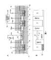
图1是表示本发明的实施方式1的FET型传感器剖面图(A)和表示电势状态的模式图(B);图2是动作状态的按顺序表示每一个电势状态的模式图。图1A中,1为典型的用硅制造的P-型半导体基板,在半导体基板1的表面,形成互相隔规定间隔的、由n+型扩散层所组成的、作为电荷供给部的输入二极管2和浮游扩散部(FD)3;并且,隔离浮游扩散部3小的间隔,形成复位二极管4。此时,在半导体基板1的上面,包括n+型扩散层上,形成由SiO2或SiO3N4所组成的绝缘膜5。1 is a sectional view (A) showing a FET sensor according to
在输入二极管2和浮游扩散部3之间的半导体基板1的表面部,与下面要叙述的栅极构造关联中,形成接通沟道(n型翻转层);其结果,构成:输入二极管2为源极、浮游扩散部3为漏极的FET型传感器。在绝缘膜5上,分别利用多晶硅或铝组成的蒸镀层,在对应于沟道始端部的输入二极管2的邻接位置上,形成输入栅极6,在对应于沟道终端部的浮游扩散部3邻接位置上,形成输出栅极7;并且,同样利用蒸镀层,在浮游扩散部3与复位二极管4之间,形成复位栅极8。In the surface portion of the
在输入栅极6、输出栅极7和复位栅极8的上面、和支持这些栅极的栅极外的绝缘膜5上,形成典型的由SiO3N4蒸镀层所组成的粘附膜10。SiO3N4膜比SiO2膜构造致密、氧的扩散系数小,所以,其本身在输入/输出栅极6、7之间形成的凹部作为传感部9而构成良好的离子感应膜。作为离子感应膜,除了SiO3N4以外,还可以利用SiO2或Au等。在该传感部9的离子感应膜上,固定与试料中的检体反应或结合的物质或固定作为检体反应催化剂的酶、抗体、微生物和核酸等的物质(图中未示)。On the
最好是,在输入二极管2和浮游扩散部3外侧的半导体基板的表面部,作为用于减少漏泄电流用的沟道阻止部(stopper),设置:比P-基板受主密度高、可以与n+扩散部2和3的施主密度抗衡的p+扩散部(图中未示);从而可以防止:电荷从输入二极管2和浮游扩散部3泄露到沟道外。Preferably, on the surface of the semiconductor substrate outside the
另外,在半导体基板1表面,在输入二极管2和复位二极管4的外侧,形成和绝缘膜5同样的硅氧化膜等所组成的比较厚的罩层11,上述的形成传感部9的粘附膜10被该罩层11覆盖,并且,在粘附膜10上,除了传感部9,还粘附形成:如磷玻璃制作的保护膜12和在其保护膜12上的、与外表面齐平面的外装膜13。In addition, on the surface of the
从图的左侧,在输入二极管2、输入栅极6、输出栅极7、浮游扩散部3、复位栅极8和复位二极管4上表面,分别形成用铝制作的电极导线;通过这些电极导线施加或检测基于测定顺序的电压(浮游扩散部3的电位)。浮游扩散部3连接在:包括能够使电极导线端子Vout安装在其自身、同一半导体基板1的源输出器放大器的电位检测和放大电路14的输入上。From the left side of the figure, on the
图2是表示根据离子浓度的测定顺序,从上述的每一个电极导线向各个部施加电压的时间。首先,在传感部9中,如图1A所示,对收容在传感部9的试料液体或相反浸渍传感部9的试料浴中,施加可变电压源Er的参照电压Vref,由此生成以此为基准的基于试料液的离子化的离子感应膜电位。Fig. 2 is a graph showing timings of voltage application from each of the above-mentioned electrode wires to respective parts according to the order of ion concentration measurement. First, in the
在对传感部9以外的各部的电极导线施加直流电压的施加电路(图中未示)中,在图2所示的初期状态(t0~t1)中,对作为电荷供给部的输入二极管2,施加约5V的反向偏压Vin,另外,对输入栅极6施加直流电压Vgin(约2V),输出栅极7维持Vgout=0。此时,对复位栅极8施加稍微延时数微秒程度的复位电压脉冲Vgr,邻接的浮游扩散部3的电位Vout是在此期间,以被Vdd吸引的形式,稍微上升,但是,在这里,不存在其前后的电位的变化,因此不存在积累电荷。In the application circuit (not shown) that applies a DC voltage to the electrode wires of each part other than the
下面,参照图1B和图3,说明离子浓度检测测定步骤。图1B是对应于图1A的各部表示上述的初期状态的本实施方式FET型传感器各部的电势和电荷量;输入二极管2的反向偏压为5V时,其部分的残存电荷量Q1微小,停止在由于输入栅极6的直流电压Vgin(约2.0V)的障壁电平的下方。另外,传感部9的参照电压Vref通过试料液(典型的是水溶液),使该传感部9的正下方的半导体基板1表面电位一定,该电位就成为确定势井深度(底面电平)b0的初期设定值,但是,在该时刻,不存在越过栅极障壁而流入的电荷。Next, referring to FIG. 1B and FIG. 3 , the ion concentration detection and measurement procedure will be described. Fig. 1B shows the potential and the amount of charge of each part of the FET type sensor of the present embodiment corresponding to each part of Fig. 1A showing the above-mentioned initial state; Below the barrier level due to the DC voltage Vgin (about 2.0 V) of the
其次,一旦到达时间t1,则到达时间t2为止的数微秒期间,使输入二极管2的反向偏压Vin降低到1V。该反向偏压的降低,带来相对的电荷供给,其积存上限电平越过约2V的输入栅极障壁,到达基于0V的输出栅极7的障壁上端附近。因此,被供给的电荷(此时为电子)也流入到输入二极管2、输入栅极6下方的半导体表面和传感部9下方的半导体表面的势井。该状态(初期电荷供给)如图3A所示。Next, once the time t1 is reached, the reverse bias voltage Vin of the
一旦到了时间t 2,则复位输入二极管2的反向偏压5V,维持数微秒。如图3B所示,相当部分的电荷Q2回到电源电路,积存在传感部9下方的势井上方的电荷,由于输入栅极6的障壁而被磨平,回到输入二极管2,加在电源电路的还流,在障壁侧部的势井内,残存对应于底面电平b0的深度的量的电荷。该残存在势井的电荷量变为:对应于水溶液离子浓度的传感部9表面电位的变化量的量。Once time t2 is reached, the
另外,如果收容在传感部9内的水溶液中的正离子浓度变高,则传感部9的表面电位变化而传感部9正下方的半导体基板1的表面电位变为低于初期设定值的值。其结果,势井的底面电平变为如图示的b1深度。在正离子浓度变低或负离子浓度变高时,相反地,底面电平的上升是不言而喻的。In addition, if the concentration of positive ions in the aqueous solution contained in the
接着,在输出栅极7里,施加5V的电压Vgout,则该输出栅极7被打开,电荷被转送到预先复位的浮游扩散部3(图3C)。在这里,如果浮游扩散部3的容量小于传感部9容量,如图所示,加大浮游扩散部3的电位变化量。在图2中,从其无电荷时的恒电压Vout,随着电荷的流入,浮游扩散部3的电位变化在最初是急剧下降,然后,慢慢地缓和而稳定在接近Gnd电位的电位。Next, when a voltage Vgout of 5 V is applied to the
这样,转送电荷后,施加在输出栅极7的电压Vgout下降为0V,而关闭输出栅极7(图3D)。如上所述,如果重复t1~t3的循环,则按顺序执行:基于从输入二极管2到势井的电荷供给/基于输入栅极6的刮平/基于输出栅极7的开放的势井残留电荷的向浮游扩散部3的转送步骤;在浮游扩散部3上,连续地积累转送电荷。In this way, after the charge is transferred, the voltage Vgout applied to the
该积累电荷量作为大的电位变化,变为:从图1A所示的浮游扩散部3的Vout输出端子向电位检测和放大电路输入的传感器输出信号SO(图2)。浮游扩散部3读取其电位之后,由于栅极电压Vgr的施加而邻接的复位栅极8被打开,所以,通过连接在+Vdd的复位二极管4的接通沟道,放出积累电荷,再度被设定为初期电位(图3E)。This accumulated charge amount becomes the sensor output signal SO (FIG. 2) input to the potential detection and amplification circuit from the Vout output terminal of the floating
在如上构成的FET型传感器中,向浮游扩散部3转送n次的情形时,和没有进行时间积累的情形相比,变为n倍,噪音只变为√n倍,S/N的比上升为√n倍,如上所述,提高灵敏度。从而,即使是基于传感部9表面电位变化的传感部9正下方势井深度的变化为微量,可以可靠地检测出其变化,可以高精度检测出:基于与检体的固定体的反应或结合的离子浓度变化,或基于固定体反应催化剂的离子浓度变化。In the case of the FET type sensor configured as above, when it is transferred to the floating diffusion part 3 n times, compared with the case where time accumulation is not performed, it becomes n times, the noise becomes only √n times, and the S/N ratio increases A factor of √n, as described above, increases sensitivity. Therefore, even if the change in the depth of the well directly below the
在该FET型传感器中,在传感部9上,固定酶的情形时,可以检测出尿素、葡萄糖、青霉素、乙酰胆碱、乙醇等。例如,检测尿素时,作为酶,利用尿素酶,可以检测出:伴随基于尿素酶的尿素分解反应的氢离子浓度变化。In this FET type sensor, when an enzyme is immobilized on the
另外,在传感部9上,固定具有与检体(靶核酸)互补的单链核酸(探针)情形时,可以高精度地检测出:检体与探针之间有无杂交的发生。从而,和PCR法比较,不增加DNA的量,简便、短时间、低成本地检测出有无杂交的发生,可以确定碱基序列。In addition, when a single-stranded nucleic acid (probe) complementary to the sample (target nucleic acid) is immobilized on the
并且,在同一半导体基板1上,包括多个该实施方式1的FET型传感器,在每一个ISFET的传感部9上,分别固定:具有与多个靶核酸互补性的单链核酸时,可以一次性地检测出多个杂交发生的有无,可以简便、短时间内确定试料中的核酸的碱基序列。In addition, when a plurality of FET-type sensors according to
(实施方式2)(Embodiment 2)
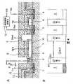
图4是表示本发明的实施方式2的FET型传感器剖面图(A)和表示基本电势状态的模式图(B);图5是表示电势状态和积累电荷推移的同样的模式图。在图中,对和图1、图3相同的部分,附以相同符号,简略或省略其说明。4 is a cross-sectional view (A) showing a FET sensor according to
该实施方式2的FET型传感器和实施方式1同样,具有以隔规定间隔形成在P-型半导体基板表面一侧的、由与基板反极性的、即N+型的扩散区域组成的输入二极管2和浮游扩散部3,以及复位二极管4,在浮游扩散部3与复位二极管4之间的绝缘膜5上,同样具有复位栅极8;由此构成:用于浮游扩散部3的复位晶体管。但是,输入二极管2与浮游扩散部3之间的绝缘膜5上的构造,在如下各点不同于实施方式1。The FET-type sensor of the second embodiment has
首先,输入栅极6′和输出栅极7′分别固定在对应于应该形成在从输入二极管2到浮游扩散部3之间的接通沟道的中间部和终端部的绝缘膜5上;为了使输入栅极6′和输出栅极7′邻接,比较窄幅而高的输出栅极7′通过覆盖比较宽幅的输入栅极6′的该邻接一侧的粘附摸10来与该输入栅极6′绝缘。输出栅极7′是其底面连接在半导体基板1上的绝缘膜5,同时,具有上方部贯通粘附摸10和保护膜12而其上端位于外装膜13内的高度。First, the input gate 6' and the output gate 7' are respectively fixed on the insulating
由此产生的输入二极管2与输入栅极6′之间的基板表面上的位置即对应于应该形成的反向沟道的输入端的位置上,形成:成为底面的绝缘膜5,同时,被夹在成为离子感应膜的输入栅极6′一侧的绝缘膜5、输入二极管2一侧的粘附摸10和保护膜12的断层而成为凹部的传感部9′。The resulting position on the substrate surface between the
下面,说明:利用该离子传感器的离子浓度检测方法。Next, an ion concentration detection method using this ion sensor will be described.
和实施方式1同样,首先,从可变电压源,对传感部9′内的水溶液施加参照电压Vref,使传感部9′正下方的半导体基板1的表面电位一定。该电位就成为势井入口的初期设定值。其次,如图2所示,对输入栅极6′施加适当的直流电压Vgin(如2.0V),固定其正下方的半导体基板1的表面电位,同时,对作为电源供给部的输入二极管2施加反向偏压Vin=5V,并对复位栅极8施加电压Vgr,设定浮游扩散部3电位的初期值。此时,输出栅极7′的电压为0V。As in
如图4B所示,输入二极管2的电压Vin5V作为充分的反向偏压,抑制该栅极内残留的电荷为很小,该电荷储存处的上端不会到达传感部9′的电平,在该部9′之后不会侵入。此时,如果水溶液中的负离子浓度变高时,传感部9′的表面电位发生变化,该传感部正下方的半导体基板1的表面电位更高于所述初期设定值b0(图4B的b2),相反地,如果负离子浓度变低或正离子浓度变高,则表面电位低于b0(图中未示)。As shown in FIG. 4B, the voltage Vin5V input to the
施加在输入二极管2的电压Vin从5V下降到1.0V,则电荷储存处量变多,其量相当于反向偏压缓和的量,其电平越过这时的传感部9′正下方的基板表面电位b0(势井入口电平),该输入二极管2的电荷供给在输入栅极6′正下方的势井(图5A)。When the voltage Vin applied to the
如果施加在输入二极管2的电压Vin再度升高到5V,则在传感部9′正下方的基板表面电位的电平中,耗尽电荷,残存相当于该电平下的势井的容量的电荷,其以外的电荷,除了该输入二极管2残留部分外经过输入二极管2还流到电源(图5B)。此时,由于负离子浓度,残留在势井的电荷量发生变化,传感部9′的表面电位的变化量转换为该电荷量是很清楚的。When the voltage Vin applied to the
接着,如果在输出栅极7′上施加5V的电压Vgout,则打开该栅极,电荷转送到电位预先维持在复位电位的浮游扩散部3(图5C)。Next, when a voltage Vgout of 5V is applied to the output gate 7', the gate is opened, and the charge is transferred to the floating
该电荷转送后,施加在输出栅极7′上的电压Vgout下降为0V,输出栅极7被关闭(图5D)。After the charge transfer, the voltage Vgout applied to the output gate 7' drops to 0V, and the
如上所述,重复图4B至图5D所示的过程,作为浮游扩散部3的电荷量积累传感部9′的表面电位的变化量。然后,积累在浮游扩散部3的电位变化量作为Vout,输入在电位检测和放大电路14,被指示而利用于记录其他的处理。As described above, the process shown in FIGS. 4B to 5D is repeated as the amount of change in the surface potential of the charge amount
电位被读取之后,浮游扩散部3是对复位栅极8施加复位栅极电压Vgr,将其部分3的电荷引导到连接在+Vdd的复位二极管4,进而被电源吸收,再次设定初期Vout值。After the potential is read, the floating
如上构成的势井入口调整型传感器中,进行N次的转送时,和没有进行时间积累的情形相比,S/N的比上升为√n倍,提高灵敏度是很清楚的。因此,即使是基于传感部9′表面电位变化的传感部9′正下方的势井的深度变化为微量,也可靠地对其进行检测,可以高灵敏度地检测出:基于与检体的固定体的反应或结合的离子浓度变化或基于固定体的催化反应的离子浓度变化。In the well inlet adjustment type sensor configured as above, when N times of transfers are performed, the S/N ratio is increased by √n times compared to the case where time accumulation is not performed, and it is clear that the sensitivity is improved. Therefore, even if the depth change of the potential well directly below the sensing part 9' due to the change in the surface potential of the sensing part 9' is slight, it can be reliably detected, and it is possible to detect with high sensitivity: The reaction of the immobilizer or the bound ion concentration change or ion concentration change based on the catalyzed reaction of the immobilizer.
在这里,如果联想图1和图3所示的实施方式1的传感器,在其传感器中,负离子浓度变高时,或正离子浓度变低时,积累电荷的势井的深度变浅或变为无,因此,转送到浮游扩散部3且残留的电荷量变少或不存在。Here, associating the sensor of
可是,在实施方式2中,邻接输入二极管2的传感部9′正下方的基板表面电位上升,与该相邻的输入栅极6正下方的基板表面电位之间的差相反地变大,在该输入栅极6正下方部分上构成势井,对负离子浓度相对高的试料,和实施方式1相比,检测灵敏度变高,或可以检测实施方式1中不能检测的试料。从而,在传感部9′上,固定与检体互补的探针时,能够以更高的灵敏度来检测出:带负电的核酸之间的结合的、负离子浓度变高的杂交的发生。However, in
通过利用实施方式2的传感器,在传感部9′上,作为探针,固定:具有与在老年痴呆病和糖尿病等的特定病中特有碱基序列的核酸互补的核酸,则可以检测出该探针是否和试料中的核酸发生杂交,由此,在发生杂交时,判断该试料中包含所述碱基序列的核酸,所以,容易、可靠地检测出有无病。By using the sensor of
另外,通过利用实施方式2的传感器,在传感部9′上,作为探针,固定:具有与试料中的规定细菌特有碱基序列的核酸互补的核酸,则可以检测出该探针是否和试料中的核酸发生杂交,由此,容易、可靠地判断出该试料中是否包含所述碱基序列的核酸,所以,可以容易、可靠地检测出试料中的细菌的有无和含量。In addition, by using the sensor of
再有,在同一个半导体基板1上,包含多个该实施方式2的FET型传感器,在各ISFET的传感部9′上,通过分别固定具有与多个靶核酸互补的单链核酸,可以一次性地检测出多个杂交发生的有无,可以简便、短时间内确定试料中的核酸的碱基序列。Furthermore, on the
另外,在上述的实施方式1和2中,说明了在本发明的FET型传感器的传感部9、9′上固定酶或核酸,检测尿素或检测杂交发生的有无的情形,但是,检测对象不限于这些,可以在传感部9、9′固定抗体和微生物等的其他的固定体,检测各种检体。另外,说明了基于杂交的检测,来检测某种疾病的有无或检测规定细菌的情形,但是,应用范围不限于这些。In addition, in the above-mentioned
(其他实施方式)(Other implementations)
在上述的实施方式1和2中,说明了在输入/输出栅极之间,形成传感部,使具有复位晶体管功能的第一形式的FET型传感器和输入/输出栅极互相接近并靠近输出一侧,在输入二极管/输入栅极之间,形成传感部;分别单独利用具有复位晶体管功能的第一形式的FET型传感器的情形和分别利用多个同一形式的FET型传感器的情形,但是,作为本发明的其他实施方式,可以形成:应该说是这些的复合型的第三形式的FET型传感器。In
该第三形式的FET型传感器是可以测定正离子和负离子双方的、测定范围广的FET型传感器;图6是表示其传感器构造的主要部分的水平剖面图,可以说是并列布置图1和图4所示的FET型传感器的传感器,对其中的相同功能的部分附以相同的参照符号的图。This third type of FET-type sensor is a FET-type sensor that can measure both positive ions and negative ions and has a wide measurement range; FIG. In the sensor of the FET type sensor shown in 4, the parts with the same function are attached with the same reference numerals.
在常规的P-型半导体所组成的基板1的表面一侧,隔规定间隔形成:与基板1相反极性的、由N+型的扩散区域组成的共通输入二极管2和浮游扩散部3,同时,浮游扩散部3被分割为第一漏极3a(第一形式的浮游扩散部)和第二漏极3b(第二形式的浮游扩散部),所述输入二极管2作为具有对应于所述分割漏极部分的共同源极,在这些源极-漏极间的基板表面部上,形成互相并列的第一、第二沟道的构成。On one side of the surface of the
并且,在构成第一和第二漏极3a、3b的浮游扩散部3的、与所述两沟道背反的一侧,与该部3隔离小间隔,同样形成由N+型扩散区域组成的共同复位二极管4,同时,在其小间隔内的基板绝缘膜(图中未示)上,固定共同复位栅极8。And, on the side of the floating
在对应于第一沟道两端的基板绝缘膜上的位置,分别固定第一形式的输入栅极6和输出栅极7,同时,在对应于该沟道的中间部(输入/输出栅极间)的基板绝缘膜上的位置上,固定由离子感应膜所组成的传感部9。结果,由该第一沟道和复位晶体管所组成的FET型传感器的纵断面(例如图6的A-A向剖面图)的构造和图1A相同。At the positions on the substrate insulating film corresponding to the two ends of the first channel, the
另外,在对应于第二沟道的中间部和终端部的基板绝缘膜上的位置,分别固定第二形式的输入栅极6′和输出栅极7′,同时,在对应于该沟道的始端部(输入二极管2/输入栅极6′间)的基板绝缘膜上的位置,形成由离子感应膜所组成的传感部9′。这样的由第二沟道和复位晶体管所组成的FET型传感器的纵断面(例如图6的B-B向剖面图)的构造和图4A相同。In addition, at the positions on the substrate insulating film corresponding to the middle portion and the terminal portion of the second channel, the input gate 6' and the output gate 7' of the second form are respectively fixed, and at the same time, at the positions corresponding to the channel At the position on the substrate insulating film at the starting end (between the
根据上述的构成,可以获得测定范围广的FET型传感器;它作为电位变化可以检测出:根据对应于作用在第一沟道和第二沟道上的每一个传感部9、9′正/负离子浓度变化的势井的深度和其势井的电荷汲出次数而相应变化的、所述浮游扩散部3在第一和第二漏极电位复位后所积累的电荷量。According to above-mentioned constitution, can obtain the FET type sensor of measuring range; It can be detected as electric potential change: The depth of the potential well whose concentration changes and the number of charge pumping out of the potential well change accordingly, the amount of charge accumulated by the floating
作为上述的复合型传感器的应用方式,在同一半导体基板上,形成多个这样的复合型传感器,由此,可以同时、有效检测出检体中的多个互补核酸构造。As an application mode of the above-mentioned composite sensor, a plurality of such composite sensors are formed on the same semiconductor substrate, whereby multiple complementary nucleic acid structures in a sample can be simultaneously and efficiently detected.
另外,作为可以获得上述的复合型传感器构造的原理,在同一半导体基板上,多个布置实施方式1和2中所示的第一和第二形式的传感器构造时,至少把输入二极管、复位栅极和复位二极管作为共同体,可以简化构造和控制。In addition, as the principle that the above-mentioned composite sensor structure can be obtained, when a plurality of sensor structures of the first and second forms shown in
在总括以上的实施例的基础上,本发明构成如下的传感器应用构造和测定方法。首先,如图7模式性表示应用构造的基本形态。On the basis of summarizing the above embodiments, the present invention constitutes the following sensor application structure and measurement method. First, Figure 7 schematically shows the basic form of the application structure.
(应用例1)(Application example 1)
在图7中,虚线圆15是试料液体收容范围,它包围:形成在上述的半导体基板表面绝缘层上的离子感应膜所组成的传感部9、9′和至少包括其周边的基板表面(绝缘膜)区域。对该范围内应包含的(隐藏在绝缘膜的下面)栅极电极、与基板反极性的二极管和其他扩散层(此时为N+层),用虚线框,代表性地,只表示有关传感器输出的浮游扩散部3,以使联想传感器全体之间的关系。In Fig. 7, dotted line circle 15 is the sample liquid accommodation area, and it surrounds: the
由SiO3N4等的离子感应膜所组成的传感部9、9′上,部分地形成金膜(或具有相当于金膜的电化学稳定性和导电性的材料膜,以下同)16,在传感部9、9′附近部(图中左侧以及左下侧),例如固定三个金凸块(或具有相当于金的电化学稳定性和导电性的材料的凸块,以下同)17a、17b、17c,通过开关18a、18b、18c,由电池Ero施加测定用或比较用电压。电池Ero的另一端子(此时为负极)连接在基板p的背面即接地电位。A gold film (or a material film with electrochemical stability and conductivity equivalent to a gold film, the same below) 16 is partially formed on the
通过利用上述构造,在金膜上,固定具有与DNA检体互补的单链核酸的末端基,同时,在包括传感部(最好是对应于半导体的接通沟道始端的传感部9′)和比较电极的区域,支持同一试料溶液,将作为浮游扩散部3的积累电位,以所述比较电极的电位为基准来测定所述的势井的汲出电荷量,由此,可以检测出所述单链核酸和检体之间有无杂交。By using the above-mentioned structure, on the gold film, the end group having the single-stranded nucleic acid complementary to the DNA sample is immobilized, and at the same time, the
(应用例2)(Application example 2)
作为本发明的另一应用方式的传感器构造,构成:如图8所示的电极悬挂下降方式。在包围半导体基板1的至少包括传感部(最好是对应于半导体接通沟道中间部的接通沟道9)区域的绝缘膜5上,由环氧玻璃等的电化学惰性材料来竖立设置·形成周壁15′,金制造的测定电极19a和比较电极19b最好是由线位移传感器来使测定电极19a带到传感部9、9′内的金膜16的正上方的位置,然后,下降而投入到试料溶液的构成。通过开关20a和20b,将基于电源Ero的电压施加在这些电极与半导体基板1的背面(接地电位)之间,或通过进一步关闭用于从金膜16串连在Ero一侧负极的开关20c,可以利用电流表A来测定此时通过的电流。As a sensor structure of another application mode of the present invention, the electrode suspension and lowering system as shown in FIG. 8 is configured. On the insulating
在上述的变形构造中,在金膜16,固定具有与DNA检体互补的单链核酸的末端基(最好是胱氨酸的SH基),同时,将试料溶液收容在周壁15′的范围内而用传感部来支持。此时,位于金膜16的正上方位置的测定电极19a与比较电极19b之间,后者(19b)被错位对其金膜16上的固定核酸不给予电影响的距离而配置的。In the above-mentioned deformed structure, on the gold film 16, the terminal group (preferably the SH group of cystine) having a single-stranded nucleic acid complementary to the DNA sample is immobilized, and at the same time, the sample solution is accommodated in the surrounding wall 15'. It is supported by the sensing part within the range. At this time, between the measurement electrode 19a and the comparison electrode 19b located directly above the gold film 16, the latter (19b) is displaced so as not to electrically affect the immobilized nucleic acid on the gold film 16.
对没入在试料溶液中的测定电极19a,DNA和所述金膜上的末端基固定核酸发生杂交之后,关闭开关20a而施加适当的如10mV~5V的电压。由此,杂交的DNA的自由末端基吸附在测定电极19a,该杂交DNA直接电连接,将Ero的电压施加在两端之间而通电。接着,接通开关20a、关闭开关20b,以位于测定电极19a相同电平溶液内位置的比较电极19b的电流为基准值,而测定。After hybridization of the DNA and the end group-immobilized nucleic acid on the gold film to the measurement electrode 19a submerged in the sample solution, the switch 20a is turned off and an appropriate voltage such as 10mV to 5V is applied. As a result, the free terminal group of the hybridized DNA is adsorbed to the measurement electrode 19a, the hybridized DNA is directly electrically connected, and a voltage of Ero is applied between both ends to conduct electricity. Next, the switch 20a is turned on and the switch 20b is turned off, and the current of the comparison electrode 19b located in the solution at the same level as the measurement electrode 19a is used as a reference value to measure.
因此,在该传感器构造中,基于原来的FET型传感器势井的电荷积累量来测定是不言而喻的,作为所述DNA电路的通电电流,测定通过测定电极的电流或利用(测定电极)与接地电位之间的电压,也可以检测出杂交的有无。Therefore, in this sensor structure, it is self-evident that the measurement is based on the charge accumulation amount of the original FET type sensor well, and as the energized current of the DNA circuit, the current passing through the measurement electrode or the current passing through the measurement electrode (measurement electrode) is measured. The presence or absence of hybridization can also be detected by the voltage between the ground potential and the ground potential.
(应用例3)(Application example 3)
如图9所示,该例不同于应用例1中所利用的传感器的构造;作为传感部9”的离子感应膜,利用氮化膜或五氧化钽膜而不利用其膜上的金凸块(图中未示)。传感部9”周边的金凸块(总括表示为17)的至少一个上,固定具有与检体DNA互补性的单链核酸的末端SH基。除了具有收容试料溶液用的周壁15′以外,其他的构造和应用例1(图7)所示的相同。As shown in FIG. 9, this example is different from the structure of the sensor used in Application Example 1; as the ion-sensitive film of the
在该测定法的实施中,通过在包括传感部9”和金电极的外周壁15′内的区域中,收容·支持试料溶液,如果在金电极上的固定核酸中有互补性的检体DNA,就会发生杂交。在该状态,如果有杂交形成的DNA,对试料溶液添加可以侵入其双螺旋链间的插入剂例如市售的「赫斯特33258」21。In the implementation of this measurement method, by accommodating and supporting the sample solution in the region including the
然后,如果通过外装膜13上的铝导线膜22对金凸块17施加负极接地的电源Ero的正电压,则由于下降的电位相当于与金凸块17接通的DNA骨骼的电阻量的下降部分,所以,插入剂21被氧化,由此,从插入剂21到金凸块1 7发生氧化·还原电流。Then, if a positive voltage of the power source Ero with the negative electrode grounded is applied to the gold bump 17 through the aluminum wire film 22 on the
其结果,在该DNA附近,发生2H+2e=H2的反应,溶液相全体的PH(H+指数)值减少。另外,可以认为:在浮游在水溶液的插入剂21上,不施加基于DNA骨架的电压,而实际上不发生氧化(H+)。在同一的传感器内或邻接·排列传感器间,可以布置几十个~几百个这样的DNA固定用金凸块,可以根据在哪一个金凸块上施加电压时发生了PH的变化来鉴定DNA。As a result, a reaction of 2H+2e=H2 occurs in the vicinity of the DNA, and the pH (H+ index) value of the entire solution phase decreases. In addition, it is considered that no voltage due to the DNA skeleton is applied to the intercalant 21 floating in the aqueous solution, and oxidation (H+) does not actually occur. Dozens to hundreds of such gold bumps for DNA immobilization can be arranged in the same sensor or between adjacent and arrayed sensors, and DNA can be identified based on the change in pH when a voltage is applied to which gold bump .
另外,不固定DNA末端基的传感部周边的金凸块可以作为比较电极来利用。PH值的测定,是以所述比较电极的电位基准,变为对应于PH变化深度的势井的汲出电荷量来测定,其测定值成为所述单链核酸与检体有无杂交的指标。In addition, the gold bumps around the sensing part where the DNA terminal group is not immobilized can be used as a comparison electrode. The measurement of the pH value is based on the potential of the comparison electrode, which becomes the amount of charge drawn from the potential well corresponding to the depth of the pH change. The measured value becomes an indicator of whether the single-stranded nucleic acid hybridizes with the sample.
另外,从插入剂21到金凸块17通过的氧化·还原电流是利用插入在电源Ero的电压施加电路的微量电流表(未图示)来测定。In addition, the oxidation/reduction current flowing from the interposer 21 to the gold bump 17 was measured with a micro ammeter (not shown) inserted in the voltage application circuit of the power supply Ero.
(应用例4)(Application example 4)
如图10所示,作为实施上述四个方法时的有利的传感器构造,在同一个半导体基板1上,并设一对FET型传感器23、24,并设置一揽子包围该一对FET型传感器的电化学惰性的丙烯酸玻璃制作的外周壁25和隔开这些传感器23、24之间、两端内接在外周壁25的隔壁26。As shown in FIG. 10, as an advantageous sensor structure when implementing the above-mentioned four methods, a pair of
由此,收容在每一个传感器23、24上的试料溶液不流通,所以,在同一个基板上邻接的两个传感器中的只是一个传感器上,固定与检体反应的靶物质,在另一个传感器上,不固定任何物质,并利用同一种试料溶液,利用另一个传感器来测定溶液·物性等的经时特性,从该另一个传感器的测定值减去该特性值,从而可以正确检测出检体与靶物质之间的合适性。当然,在两个传感器中,收容不同的试料溶液而互相没有影响地各自测定,也是可以的。As a result, the sample solution contained in each of the
(产业上的可利用性)(industrial availability)
如上所述,根据本发明,在通过并设复位晶体管,重复电荷转送过程而高灵敏度化的FET型传感器中,传感部可以在广的范围内、以高灵敏度检测出作为试料或检体反应结果的正离子或负离子浓度的变化。As described above, according to the present invention, in the FET type sensor whose sensitivity is increased by repeating the charge transfer process by providing a reset transistor in parallel, the sensor part can detect the A change in the concentration of positive or negative ions that results from a reaction.
另外,通过分别布置多个第一形式、第二形式的FET型传感器和两个形式的复合形式或在同一个半导体基板上布置多个复合形式的构成,在物质的电化学的测定、特别是在生物化学领域中,判断所测定的试料中是否包含给定的细菌或具有疾病特有碱基序列的核酸,能够容易、可靠地检测出细菌或疾病的有无和细菌的含量;并且,在测定环境荷尔蒙或二恶英关联物质上,开辟了新的道路。In addition, by arranging a plurality of FET-type sensors of the first form and the second form and a composite form of the two forms or arranging a plurality of composite forms on the same semiconductor substrate, the electrochemical determination of substances, especially In the field of biochemistry, judging whether the measured sample contains a given bacterium or a nucleic acid with a disease-specific base sequence can easily and reliably detect the presence or absence of bacteria or disease and the content of bacteria; and, in It has opened up a new way for the determination of environmental hormones or dioxin-related substances.
通过在FET型传感器中,尤其优选利用金凸块或金电极的本发明的DNA测定方法,有助于简便、正确·稳定的DNA鉴定。In the FET type sensor, the DNA measurement method of the present invention using gold bumps or gold electrodes is particularly preferable, which contributes to simple, accurate and stable DNA identification.
Claims (6)
Applications Claiming Priority (2)
| Application Number | Priority Date | Filing Date | Title |
|---|---|---|---|
| JP2001351657 | 2001-11-16 | ||
| JP351657/2001 | 2001-11-16 |
Publications (2)
| Publication Number | Publication Date |
|---|---|
| CN1585896A CN1585896A (en) | 2005-02-23 |
| CN100429509Ctrue CN100429509C (en) | 2008-10-29 |
Family
ID=19163939
Family Applications (1)
| Application Number | Title | Priority Date | Filing Date |
|---|---|---|---|
| CNB028225392AExpired - LifetimeCN100429509C (en) | 2001-11-16 | 2002-11-11 | FET type sensor |
Country Status (4)
| Country | Link |
|---|---|
| US (1) | US7049645B2 (en) |
| JP (1) | JP4195859B2 (en) |
| CN (1) | CN100429509C (en) |
| WO (1) | WO2003042683A1 (en) |
Families Citing this family (95)
| Publication number | Priority date | Publication date | Assignee | Title |
|---|---|---|---|---|
| GB0105831D0 (en) | 2001-03-09 | 2001-04-25 | Toumaz Technology Ltd | Method for dna sequencing utilising enzyme linked field effect transistors |
| US8114591B2 (en) | 2001-03-09 | 2012-02-14 | Dna Electronics Ltd. | Sensing apparatus and method |
| GB0211564D0 (en) | 2002-05-21 | 2002-06-26 | Tournaz Technology Ltd | Reference circuit |
| US7368085B2 (en)* | 2003-12-04 | 2008-05-06 | Honeywell International Inc. | Analyte detector |
| US20050218464A1 (en)* | 2004-03-18 | 2005-10-06 | Holm-Kennedy James W | Biochemical ultrasensitive charge sensing |
| ITTO20040386A1 (en)* | 2004-06-09 | 2004-09-09 | Infm Istituto Naz Per La Fisi | FIELD-EFFECTIVE DEVICE FOR THE DETECTION OF SMALL QUANTITIES OF ELECTRIC CHARGE, SUCH AS THOSE GENERATED IN BIOMOLECULAR PROCESSES, IMMOBILIZED NEAR THE SURFACE. |
| US8536661B1 (en) | 2004-06-25 | 2013-09-17 | University Of Hawaii | Biosensor chip sensor protection methods |
| WO2007008246A2 (en) | 2004-11-12 | 2007-01-18 | The Board Of Trustees Of The Leland Stanford Junior University | Charge perturbation detection system for dna and other molecules |
| JP4678676B2 (en)* | 2004-12-10 | 2011-04-27 | 株式会社堀場製作所 | Method or apparatus for measuring physical or chemical phenomena |
| WO2006095252A1 (en)* | 2005-03-08 | 2006-09-14 | National Research Council Of Canada | Electrostatically regulated atomic scale electroconductivity device |
| US7826980B2 (en)* | 2005-03-11 | 2010-11-02 | National University Corporation Toyohashi University Of Technology | Cumulative chemical/physical phenomenon detecting apparatus |
| JP4641444B2 (en)* | 2005-03-31 | 2011-03-02 | 株式会社堀場製作所 | Potential measurement device for physical or chemical phenomena |
| US7629174B2 (en)* | 2005-08-26 | 2009-12-08 | Honeywell International Inc. | Analyte detector |
| WO2007108465A1 (en)* | 2006-03-20 | 2007-09-27 | National University Corporation Toyohashi University Of Technology | Accumulated type chemical/physical phenomenon detection method and device thereof |
| US11339430B2 (en) | 2007-07-10 | 2022-05-24 | Life Technologies Corporation | Methods and apparatus for measuring analytes using large scale FET arrays |
| US8349167B2 (en) | 2006-12-14 | 2013-01-08 | Life Technologies Corporation | Methods and apparatus for detecting molecular interactions using FET arrays |
| CA2672315A1 (en) | 2006-12-14 | 2008-06-26 | Ion Torrent Systems Incorporated | Methods and apparatus for measuring analytes using large scale fet arrays |
| US8262900B2 (en) | 2006-12-14 | 2012-09-11 | Life Technologies Corporation | Methods and apparatus for measuring analytes using large scale FET arrays |
| KR101176547B1 (en)* | 2006-12-20 | 2012-08-24 | 리전츠 오브 더 유니버스티 오브 미네소타 | Apparatus and method of detecting ionic materials with reduced noise |
| WO2009011164A1 (en)* | 2007-07-19 | 2009-01-22 | Renesas Technology Corp. | Semiconductor device, and its manufacturing method |
| US8762887B2 (en)* | 2008-06-06 | 2014-06-24 | Apple Inc. | Browsing or searching user interfaces and other aspects |
| GB2461128B (en)* | 2008-06-25 | 2010-12-15 | Ion Torrent Systems Inc | ChemFET Arrays for Nucleic Acid Sequencing |
| CN102203282B (en) | 2008-06-25 | 2014-04-30 | 生命技术公司 | Methods and apparatus for measuring analytes using large scale FET arrays |
| US20100035252A1 (en)* | 2008-08-08 | 2010-02-11 | Ion Torrent Systems Incorporated | Methods for sequencing individual nucleic acids under tension |
| US20100301398A1 (en) | 2009-05-29 | 2010-12-02 | Ion Torrent Systems Incorporated | Methods and apparatus for measuring analytes |
| US20100137143A1 (en)* | 2008-10-22 | 2010-06-03 | Ion Torrent Systems Incorporated | Methods and apparatus for measuring analytes |
| EP2342552B1 (en)* | 2008-10-22 | 2022-09-14 | Life Technologies Corporation | Floating gate chemical field effect transistor array with bilayer gate dielectric |
| DE102008043858A1 (en)* | 2008-11-19 | 2010-05-20 | Robert Bosch Gmbh | Method for passivating a field effect transistor |
| JP2010122090A (en)* | 2008-11-20 | 2010-06-03 | Rohm Co Ltd | Ion image sensor and damage measuring device |
| CN101592627B (en)* | 2009-03-19 | 2012-12-05 | 中国科学院苏州纳米技术与纳米仿生研究所 | Method for manufacturing and integrating multichannel high-sensitive biosensor |
| US8673627B2 (en) | 2009-05-29 | 2014-03-18 | Life Technologies Corporation | Apparatus and methods for performing electrochemical reactions |
| US8776573B2 (en) | 2009-05-29 | 2014-07-15 | Life Technologies Corporation | Methods and apparatus for measuring analytes |
| US20120261274A1 (en) | 2009-05-29 | 2012-10-18 | Life Technologies Corporation | Methods and apparatus for measuring analytes |
| US8574835B2 (en) | 2009-05-29 | 2013-11-05 | Life Technologies Corporation | Scaffolded nucleic acid polymer particles and methods of making and using |
| JPWO2011152209A1 (en)* | 2010-06-03 | 2013-07-25 | シャープ株式会社 | Ion sensor and display device |
| AU2011226792A1 (en) | 2010-06-11 | 2012-01-12 | Life Technologies Corporation | Alternative nucleotide flows in sequencing-by-synthesis methods |
| TWI539172B (en) | 2010-06-30 | 2016-06-21 | 生命技術公司 | Methods and apparatus for testing isfet arrays |
| WO2012003363A1 (en)* | 2010-06-30 | 2012-01-05 | Life Technologies Corporation | Ion-sensing charge-accumulation circuits and methods |
| JP2013540259A (en) | 2010-06-30 | 2013-10-31 | ライフ テクノロジーズ コーポレーション | Array column integrator |
| US11307166B2 (en) | 2010-07-01 | 2022-04-19 | Life Technologies Corporation | Column ADC |
| EP2589065B1 (en) | 2010-07-03 | 2015-08-19 | Life Technologies Corporation | Chemically sensitive sensor with lightly doped drains |
| US20120045368A1 (en) | 2010-08-18 | 2012-02-23 | Life Technologies Corporation | Chemical Coating of Microwell for Electrochemical Detection Device |
| WO2012036679A1 (en) | 2010-09-15 | 2012-03-22 | Life Technologies Corporation | Methods and apparatus for measuring analytes |
| US8796036B2 (en) | 2010-09-24 | 2014-08-05 | Life Technologies Corporation | Method and system for delta double sampling |
| WO2012118555A1 (en) | 2010-12-29 | 2012-09-07 | Life Technologies Corporation | Time-warped background signal for sequencing-by-synthesis operations |
| WO2012092515A2 (en) | 2010-12-30 | 2012-07-05 | Life Technologies Corporation | Methods, systems, and computer readable media for nucleic acid sequencing |
| US20130060482A1 (en) | 2010-12-30 | 2013-03-07 | Life Technologies Corporation | Methods, systems, and computer readable media for making base calls in nucleic acid sequencing |
| EP2658999B1 (en) | 2010-12-30 | 2019-03-13 | Life Technologies Corporation | Models for analyzing data from sequencing-by-synthesis operations |
| EP2694675B1 (en) | 2011-04-08 | 2018-01-24 | Life Technologies Corporation | Phase-protecting reagent flow orderings for use in sequencing-by-synthesis |
| US9482641B2 (en) | 2011-08-12 | 2016-11-01 | National University Corporation Toyohashi University Of Technology | Device and method for detecting chemical and physical phenomena |
| EP2745108B1 (en) | 2011-08-18 | 2019-06-26 | Life Technologies Corporation | Methods, systems, and computer readable media for making base calls in nucleic acid sequencing |
| JP2013050426A (en)* | 2011-08-31 | 2013-03-14 | Chiba Univ | Method of detecting influenza virus rna using fet-type sensor |
| US10704164B2 (en) | 2011-08-31 | 2020-07-07 | Life Technologies Corporation | Methods, systems, computer readable media, and kits for sample identification |
| US20150087537A1 (en) | 2011-08-31 | 2015-03-26 | Life Technologies Corporation | Methods, Systems, Computer Readable Media, and Kits for Sample Identification |
| WO2013074796A1 (en)* | 2011-11-15 | 2013-05-23 | The Board Of Trustees Of The University Of Illinois | Thermal control of droplets by nanoscale field effect transistors |
| DE102012110871A1 (en)* | 2011-11-17 | 2013-06-20 | Endress + Hauser Conducta Gesellschaft für Mess- und Regeltechnik mbH + Co. KG | Sensor for detecting a measured variable of a medium |
| US9970984B2 (en) | 2011-12-01 | 2018-05-15 | Life Technologies Corporation | Method and apparatus for identifying defects in a chemical sensor array |
| US8821798B2 (en) | 2012-01-19 | 2014-09-02 | Life Technologies Corporation | Titanium nitride as sensing layer for microwell structure |
| US8747748B2 (en) | 2012-01-19 | 2014-06-10 | Life Technologies Corporation | Chemical sensor with conductive cup-shaped sensor surface |
| US9194840B2 (en) | 2012-01-19 | 2015-11-24 | Life Technologies Corporation | Sensor arrays and methods for making same |
| US9646132B2 (en) | 2012-05-11 | 2017-05-09 | Life Technologies Corporation | Models for analyzing data from sequencing-by-synthesis operations |
| US8786331B2 (en) | 2012-05-29 | 2014-07-22 | Life Technologies Corporation | System for reducing noise in a chemical sensor array |
| US9599586B2 (en)* | 2012-08-27 | 2017-03-21 | Infineon Technologies Ag | Ion sensor |
| US10329608B2 (en) | 2012-10-10 | 2019-06-25 | Life Technologies Corporation | Methods, systems, and computer readable media for repeat sequencing |
| US9080968B2 (en) | 2013-01-04 | 2015-07-14 | Life Technologies Corporation | Methods and systems for point of use removal of sacrificial material |
| US9841398B2 (en) | 2013-01-08 | 2017-12-12 | Life Technologies Corporation | Methods for manufacturing well structures for low-noise chemical sensors |
| US8962366B2 (en) | 2013-01-28 | 2015-02-24 | Life Technologies Corporation | Self-aligned well structures for low-noise chemical sensors |
| US9045795B2 (en)* | 2013-03-13 | 2015-06-02 | Life Technologies Corporation | Methods to control dissolved gas |
| US8963216B2 (en) | 2013-03-13 | 2015-02-24 | Life Technologies Corporation | Chemical sensor with sidewall spacer sensor surface |
| US8841217B1 (en) | 2013-03-13 | 2014-09-23 | Life Technologies Corporation | Chemical sensor with protruded sensor surface |
| US20140296080A1 (en) | 2013-03-14 | 2014-10-02 | Life Technologies Corporation | Methods, Systems, and Computer Readable Media for Evaluating Variant Likelihood |
| US9116117B2 (en) | 2013-03-15 | 2015-08-25 | Life Technologies Corporation | Chemical sensor with sidewall sensor surface |
| EP2972280B1 (en) | 2013-03-15 | 2021-09-29 | Life Technologies Corporation | Chemical sensor with consistent sensor surface areas |
| EP2972279B1 (en) | 2013-03-15 | 2021-10-06 | Life Technologies Corporation | Chemical sensors with consistent sensor surface areas |
| JP6671274B2 (en) | 2013-03-15 | 2020-03-25 | ライフ テクノロジーズ コーポレーション | Chemical device with thin conductive element |
| US9835585B2 (en) | 2013-03-15 | 2017-12-05 | Life Technologies Corporation | Chemical sensor with protruded sensor surface |
| US20140336063A1 (en) | 2013-05-09 | 2014-11-13 | Life Technologies Corporation | Windowed Sequencing |
| US10458942B2 (en) | 2013-06-10 | 2019-10-29 | Life Technologies Corporation | Chemical sensor array having multiple sensors per well |
| CN105683980B (en) | 2013-10-04 | 2018-08-24 | 生命科技股份有限公司 | The method and system of effect model stage by stage is established in using the sequencing for terminating chemical substance |
| US9395326B2 (en) | 2013-11-01 | 2016-07-19 | Taiwan Semiconductor Manufacturing Company Limited | FET sensing cell and method of improving sensitivity of the same |
| US9476853B2 (en) | 2013-12-10 | 2016-10-25 | Life Technologies Corporation | System and method for forming microwells |
| CN103969314B (en)* | 2014-05-06 | 2017-02-15 | 中国农业科学院农业信息研究所 | Multi-parameter ionic sensor and preparation method thereof, as well as multi-parameter ionic sensor chip and monitoring system |
| US10676787B2 (en) | 2014-10-13 | 2020-06-09 | Life Technologies Corporation | Methods, systems, and computer-readable media for accelerated base calling |
| JP6228098B2 (en) | 2014-10-20 | 2017-11-08 | シャープ株式会社 | Chemical / physical phenomenon detection device and manufacturing method thereof |
| DE102014115980B4 (en)* | 2014-11-03 | 2022-06-23 | Infineon Technologies Ag | Device for analyzing ion kinetics in dielectrics |
| CN107407656B (en) | 2014-12-18 | 2020-04-07 | 生命科技公司 | Method and apparatus for measuring analytes using large scale FET arrays |
| KR102593647B1 (en) | 2014-12-18 | 2023-10-26 | 라이프 테크놀로지스 코포레이션 | High data rate integrated circuit with transmitter configuration |
| US10077472B2 (en) | 2014-12-18 | 2018-09-18 | Life Technologies Corporation | High data rate integrated circuit with power management |
| CN114540475B (en) | 2015-05-14 | 2025-07-29 | 生命科技公司 | Barcode sequences and related systems and methods |
| JP6307058B2 (en)* | 2015-12-03 | 2018-04-04 | シャープ株式会社 | Ion concentration sensor and ion concentration measuring method |
| JP6447925B2 (en) | 2015-12-15 | 2019-01-09 | シャープ株式会社 | Ion concentration sensor |
| US10619205B2 (en) | 2016-05-06 | 2020-04-14 | Life Technologies Corporation | Combinatorial barcode sequences, and related systems and methods |
| WO2019225660A1 (en)* | 2018-05-25 | 2019-11-28 | 公立大学法人大阪 | Chemical sensor |
| JP7634361B2 (en)* | 2020-12-25 | 2025-02-21 | 浜松ホトニクス株式会社 | Ion sensor and method for manufacturing the same |
| CN116925902A (en)* | 2022-04-08 | 2023-10-24 | 港岫科技(上海)有限公司 | RNA detection device |
Citations (8)
| Publication number | Priority date | Publication date | Assignee | Title |
|---|---|---|---|---|
| JPS60247151A (en)* | 1984-05-23 | 1985-12-06 | Fujitsu Ltd | Fet biosensor |
| JPH06249826A (en)* | 1993-02-26 | 1994-09-09 | Tokyo Gas Co Ltd | Fet sensor |
| JPH08278281A (en)* | 1995-04-07 | 1996-10-22 | Hitachi Ltd | Field effect type chemical substance detection device and DNA sequencer using the same |
| JP2001033274A (en)* | 1999-07-23 | 2001-02-09 | Horiba Ltd | Physical/chemical two-dimentional distribution measuring device |
| US6203981B1 (en)* | 1996-04-17 | 2001-03-20 | Motorola, Inc. | Transistor-based molecular detection apparatus and method |
| US6255678B1 (en)* | 1997-05-29 | 2001-07-03 | Horiba, Ltd. | Apparatus for measuring physical and chemical phenomena |
| JP2002009274A (en)* | 2000-06-21 | 2002-01-11 | Horiba Ltd | Chemical CCD sensor |
| JP2002098667A (en)* | 2000-09-27 | 2002-04-05 | Japan Science & Technology Corp | Cumulative chemical / physical phenomenon detector |
Family Cites Families (3)
| Publication number | Priority date | Publication date | Assignee | Title |
|---|---|---|---|---|
| US4156818A (en)* | 1975-12-23 | 1979-05-29 | International Business Machines Corporation | Operating circuitry for semiconductor charge coupled devices |
| US4275315A (en)* | 1979-10-10 | 1981-06-23 | Hughes Aircraft Company | Charge summing filter aperture corrector |
| JPS61131854U (en)* | 1985-02-06 | 1986-08-18 |
- 2002
- 2002-11-11CNCNB028225392Apatent/CN100429509C/ennot_activeExpired - Lifetime
- 2002-11-11WOPCT/JP2002/011752patent/WO2003042683A1/enactiveApplication Filing
- 2002-11-11USUS10/495,808patent/US7049645B2/ennot_activeExpired - Lifetime
- 2002-11-11JPJP2003544466Apatent/JP4195859B2/ennot_activeExpired - Lifetime
Patent Citations (8)
| Publication number | Priority date | Publication date | Assignee | Title |
|---|---|---|---|---|
| JPS60247151A (en)* | 1984-05-23 | 1985-12-06 | Fujitsu Ltd | Fet biosensor |
| JPH06249826A (en)* | 1993-02-26 | 1994-09-09 | Tokyo Gas Co Ltd | Fet sensor |
| JPH08278281A (en)* | 1995-04-07 | 1996-10-22 | Hitachi Ltd | Field effect type chemical substance detection device and DNA sequencer using the same |
| US6203981B1 (en)* | 1996-04-17 | 2001-03-20 | Motorola, Inc. | Transistor-based molecular detection apparatus and method |
| US6255678B1 (en)* | 1997-05-29 | 2001-07-03 | Horiba, Ltd. | Apparatus for measuring physical and chemical phenomena |
| JP2001033274A (en)* | 1999-07-23 | 2001-02-09 | Horiba Ltd | Physical/chemical two-dimentional distribution measuring device |
| JP2002009274A (en)* | 2000-06-21 | 2002-01-11 | Horiba Ltd | Chemical CCD sensor |
| JP2002098667A (en)* | 2000-09-27 | 2002-04-05 | Japan Science & Technology Corp | Cumulative chemical / physical phenomenon detector |
Also Published As
| Publication number | Publication date |
|---|---|
| WO2003042683A1 (en) | 2003-05-22 |
| JPWO2003042683A1 (en) | 2005-03-10 |
| US20050062093A1 (en) | 2005-03-24 |
| JP4195859B2 (en) | 2008-12-17 |
| CN1585896A (en) | 2005-02-23 |
| US7049645B2 (en) | 2006-05-23 |
Similar Documents
| Publication | Publication Date | Title |
|---|---|---|
| CN100429509C (en) | FET type sensor | |
| Macchia et al. | About the amplification factors in organic bioelectronic sensors | |
| US10481123B2 (en) | Ion-sensing charge-accumulation circuits and methods | |
| JP3874772B2 (en) | Biologically related substance measuring apparatus and measuring method | |
| EP3586115B1 (en) | Analyte detector for detecting at least one analyte in at least one fluid sample | |
| KR101056385B1 (en) | Detection element | |
| TWI569025B (en) | Methods and apparatus for testing isfet arrays | |
| JP5876044B2 (en) | Chemically sensitive sensor with lightly doped drain | |
| JP4768226B2 (en) | FET sensor with gate electrode specially configured for sensitive detection of analyte | |
| US20060197118A1 (en) | Detection of molecular interactions using a field effect transistor | |
| US10481126B2 (en) | Electrolyte-gated transistors for detection of molecules | |
| WO2013049463A2 (en) | Double gate ion sensitive field effect transistor | |
| Wu et al. | Sequentially multiplexed amperometry for electrochemical biosensors | |
| Ltith et al. | Penicillin detection by means of silicon-based field-effect structures | |
| TWI777376B (en) | Biological detecting chip and biological detecting method | |
| JP2013050426A (en) | Method of detecting influenza virus rna using fet-type sensor | |
| WO2016111237A1 (en) | Target substance detection method using fet biosensor | |
| Estrela et al. | Application of thin film transistors to label-free electrical biosensors | |
| JP2019002727A (en) | Transistor for sensor | |
| KR20240171119A (en) | Biosensor |
Legal Events
| Date | Code | Title | Description |
|---|---|---|---|
| C06 | Publication | ||
| PB01 | Publication | ||
| C10 | Entry into substantive examination | ||
| SE01 | Entry into force of request for substantive examination | ||
| C14 | Grant of patent or utility model | ||
| GR01 | Patent grant | ||
| CX01 | Expiry of patent term | ||
| CX01 | Expiry of patent term | Granted publication date:20081029 |