CN100420011C - Interconnect structure for integrated circuit and SRAM cell - Google Patents
Interconnect structure for integrated circuit and SRAM cellDownload PDFInfo
- Publication number
- CN100420011C CN100420011CCNB2006100765140ACN200610076514ACN100420011CCN 100420011 CCN100420011 CCN 100420011CCN B2006100765140 ACNB2006100765140 ACN B2006100765140ACN 200610076514 ACN200610076514 ACN 200610076514ACN 100420011 CCN100420011 CCN 100420011C
- Authority
- CN
- China
- Prior art keywords
- contact region
- cross
- layer
- coupled
- nmos transistor
- Prior art date
- Legal status (The legal status is an assumption and is not a legal conclusion. Google has not performed a legal analysis and makes no representation as to the accuracy of the status listed.)
- Active
Links
- 239000010410layerSubstances0.000claimsabstractdescription133
- 239000004020conductorSubstances0.000claimsabstractdescription35
- 230000003068static effectEffects0.000claimsabstractdescription17
- 239000004065semiconductorSubstances0.000claimsabstractdescription16
- 239000000758substrateSubstances0.000claimsabstractdescription9
- 239000011229interlayerSubstances0.000claimsabstractdescription7
- 229910052751metalInorganic materials0.000claimsdescription52
- 239000002184metalSubstances0.000claimsdescription52
- 238000003860storageMethods0.000claimsdescription13
- 230000000295complement effectEffects0.000claimsdescription10
- 125000006850spacer groupChemical group0.000claimsdescription9
- 229910021420polycrystalline siliconInorganic materials0.000description9
- 229920005591polysiliconPolymers0.000description7
- 238000000034methodMethods0.000description5
- 238000010586diagramMethods0.000description4
- 238000004519manufacturing processMethods0.000description4
- 239000012535impuritySubstances0.000description3
- 229910044991metal oxideInorganic materials0.000description3
- 150000004706metal oxidesChemical class0.000description3
- 239000010949copperSubstances0.000description2
- 238000000151depositionMethods0.000description2
- 230000008021depositionEffects0.000description2
- 230000009977dual effectEffects0.000description2
- 239000007943implantSubstances0.000description2
- 238000001465metallisationMethods0.000description2
- 238000000206photolithographyMethods0.000description2
- RYGMFSIKBFXOCR-UHFFFAOYSA-NCopperChemical compound[Cu]RYGMFSIKBFXOCR-UHFFFAOYSA-N0.000description1
- NRTOMJZYCJJWKI-UHFFFAOYSA-NTitanium nitrideChemical compound[Ti]#NNRTOMJZYCJJWKI-UHFFFAOYSA-N0.000description1
- 238000006243chemical reactionMethods0.000description1
- 229910052802copperInorganic materials0.000description1
- 238000005530etchingMethods0.000description1
- 238000001459lithographyMethods0.000description1
- 238000005498polishingMethods0.000description1
- HBMJWWWQQXIZIP-UHFFFAOYSA-Nsilicon carbideChemical compound[Si+]#[C-]HBMJWWWQQXIZIP-UHFFFAOYSA-N0.000description1
- 239000000126substanceSubstances0.000description1
- 239000013589supplementSubstances0.000description1
- MZLGASXMSKOWSE-UHFFFAOYSA-Ntantalum nitrideChemical compound[Ta]#NMZLGASXMSKOWSE-UHFFFAOYSA-N0.000description1
- WFKWXMTUELFFGS-UHFFFAOYSA-NtungstenChemical compound[W]WFKWXMTUELFFGS-UHFFFAOYSA-N0.000description1
- 229910052721tungstenInorganic materials0.000description1
- 239000010937tungstenSubstances0.000description1
Images


Classifications
- H—ELECTRICITY
- H01—ELECTRIC ELEMENTS
- H01L—SEMICONDUCTOR DEVICES NOT COVERED BY CLASS H10
- H01L23/00—Details of semiconductor or other solid state devices
- H01L23/52—Arrangements for conducting electric current within the device in operation from one component to another, i.e. interconnections, e.g. wires, lead frames
- H01L23/522—Arrangements for conducting electric current within the device in operation from one component to another, i.e. interconnections, e.g. wires, lead frames including external interconnections consisting of a multilayer structure of conductive and insulating layers inseparably formed on the semiconductor body
- H01L23/5226—Via connections in a multilevel interconnection structure
- H—ELECTRICITY
- H01—ELECTRIC ELEMENTS
- H01L—SEMICONDUCTOR DEVICES NOT COVERED BY CLASS H10
- H01L23/00—Details of semiconductor or other solid state devices
- H01L23/52—Arrangements for conducting electric current within the device in operation from one component to another, i.e. interconnections, e.g. wires, lead frames
- H01L23/522—Arrangements for conducting electric current within the device in operation from one component to another, i.e. interconnections, e.g. wires, lead frames including external interconnections consisting of a multilayer structure of conductive and insulating layers inseparably formed on the semiconductor body
- H01L23/528—Layout of the interconnection structure
- H—ELECTRICITY
- H10—SEMICONDUCTOR DEVICES; ELECTRIC SOLID-STATE DEVICES NOT OTHERWISE PROVIDED FOR
- H10B—ELECTRONIC MEMORY DEVICES
- H10B10/00—Static random access memory [SRAM] devices
- H—ELECTRICITY
- H10—SEMICONDUCTOR DEVICES; ELECTRIC SOLID-STATE DEVICES NOT OTHERWISE PROVIDED FOR
- H10B—ELECTRONIC MEMORY DEVICES
- H10B10/00—Static random access memory [SRAM] devices
- H10B10/12—Static random access memory [SRAM] devices comprising a MOSFET load element
- H—ELECTRICITY
- H01—ELECTRIC ELEMENTS
- H01L—SEMICONDUCTOR DEVICES NOT COVERED BY CLASS H10
- H01L2924/00—Indexing scheme for arrangements or methods for connecting or disconnecting semiconductor or solid-state bodies as covered by H01L24/00
- H01L2924/0001—Technical content checked by a classifier
- H01L2924/0002—Not covered by any one of groups H01L24/00, H01L24/00 and H01L2224/00
Landscapes
- Physics & Mathematics (AREA)
- Condensed Matter Physics & Semiconductors (AREA)
- General Physics & Mathematics (AREA)
- Engineering & Computer Science (AREA)
- Computer Hardware Design (AREA)
- Microelectronics & Electronic Packaging (AREA)
- Power Engineering (AREA)
- Geometry (AREA)
- Internal Circuitry In Semiconductor Integrated Circuit Devices (AREA)
- Semiconductor Memories (AREA)
Abstract
Description
Translated fromChinese技术领域technical field
本发明是有关于一种半导体设计,特别是有关于一种集成电路的内连线结构。The present invention relates to a semiconductor design, in particular to an interconnection structure of an integrated circuit.
背景技术Background technique
随着半导体技术演进至深次微米(deep sub-micron)的时代,晶片内的电路结构亦变得更加拥挤。举例来说,静态随机存取存储(static random access memory;SRAM)单元的电路结构已变得如此稠密,以致于完成所有必要的布线变得额外地困难。从一金属层至另一金属层的接触区(contact)需要内连线结构。在双镶嵌金属制程(dual damascene metallization process)中,导电材料被注入介层孔(via)及沟槽(trench),而多余的部分则以诸如:化学机械研磨法(chemical mechanical polishing;CMP)磨除。接触区(由导电材料注入介层孔而形成)提供垂直连接,而沟槽(亦由导电材料所填充)则提供侧边的垫片及导线。在集成电路的所有以微影技术(lithography)及蚀刻(etching)来形成的半导体结构中,介层孔通常为最小的特性结构。As semiconductor technology evolves into the era of deep sub-micron, the circuit structure in the chip becomes more crowded. For example, the circuit structure of static random access memory (SRAM) cells has become so dense that it becomes extra difficult to perform all the necessary wiring. Contacts from one metal layer to another require interconnect structures. In the dual damascene metallization process (dual damascene metallization process), the conductive material is injected into the via and the trench (trench), and the excess part is polished by chemical mechanical polishing (CMP). remove. Contact areas (formed by injecting conductive material into vias) provide vertical connections, while trenches (also filled with conductive material) provide side pads and wires. In all semiconductor structures formed by lithography and etching in integrated circuits, vias are usually the smallest characteristic structures.
因为有限的光学微影(photolithography)技术,持续缩小的介层接触区对集成电路制造形成一大挑战。若介层孔没对准,整个内连线结构便无法形成。因此,随着集成电路尺寸持续缩小,提供介层孔适当调校空间的内连线结构便成为首要之务。The ever-shrinking via contact area poses a major challenge to integrated circuit fabrication due to limited photolithography techniques. If the vias are misaligned, the entire interconnect structure cannot be formed. Therefore, as the size of integrated circuits continues to shrink, an interconnection structure that provides proper adjustment space for vias has become a top priority.
发明内容Contents of the invention
为获致上述的目的,本发明提出一种形成于半导体基底上的集成电路内连线结构。其中,第一导体层形成于上述半导体基底上。第一介层接触区形成于上述第一导体层上。第二介层接触区形成于上述第一介层接触区上。第二导体层形成于上述第二介层接触区上。第一与第二介层接触区其中之一的横截面大体上大于另一横截面以改善其着陆空间(landing margin),因而无需在第一与第二介层接触区之间使用着陆垫片(landing pad)。To achieve the above objectives, the present invention provides an integrated circuit interconnection structure formed on a semiconductor substrate. Wherein, the first conductor layer is formed on the above-mentioned semiconductor substrate. The first interlayer contact region is formed on the first conductor layer. The second via contact region is formed on the first via contact region. The second conductor layer is formed on the above-mentioned second interlayer contact area. The cross-section of one of the first and second via contact regions is substantially larger than the other to improve its landing margin, thereby eliminating the need for a landing pad between the first and second via contact regions (landing pad).
本发明所述的集成电路的内连线结构,上述第一介层接触区或上述第二介层接触区具有一大体上与纵向方向一致的侧壁。In the interconnection structure of an integrated circuit according to the present invention, the first via contact region or the second via contact region has a sidewall substantially in line with the longitudinal direction.
本发明所述的集成电路的内连线结构,上述第一介层接触区的横截面大体上大于上述第二介层接触区的横截面。According to the interconnection structure of the integrated circuit of the present invention, the cross-section of the first via contact region is substantially larger than the cross-section of the second via contact region.
本发明所述的集成电路的内连线结构,从俯视图来看,其中上述第一介层接触区的横截面边界大得足以围绕上述第二介层接触区的横截面边界。According to the interconnection structure of the integrated circuit of the present invention, viewed from the top view, the cross-sectional boundary of the first via contact region is large enough to surround the cross-sectional boundary of the second via contact region.
本发明还提供一种集成电路的内连线结构,所述集成电路的内连线结构包括:一第一导体层,形成于一第一金属层上;一第一介层接触区,直接耦接至上述第一导体层,形成于上述第一金属层上;一第二导体层,形成于一第二金属层上;一第二介层接触区,直接耦接至上述第二导体层,形成于上述第二金属层上;以及一个以上的中间介层接触区,耦接于上述第一介层接触区与上述第二介层接触区之间,所述中间介层接触区在一个以上的中间金属层之上,介于上述第一金属层与上述第二金属层之间,其中上述第一介层接触区、第二介层接触区、以及中间介层接触区之一横截面大体上大于其他的横截面,以改善着陆空间,因而无需在其间使用一着陆垫片。The present invention also provides an interconnection structure of an integrated circuit. The interconnection structure of the integrated circuit includes: a first conductor layer formed on a first metal layer; a first interlayer contact region directly coupled connected to the first conductor layer, formed on the first metal layer; a second conductor layer, formed on a second metal layer; a second interlayer contact region, directly coupled to the second conductor layer, formed on the above-mentioned second metal layer; and more than one interposer contact region, coupled between the above-mentioned first via layer contact region and the above-mentioned second via layer contact region, the interposer contact region is more than one on the intermediate metal layer, between the above-mentioned first metal layer and the above-mentioned second metal layer, wherein the cross-section of one of the above-mentioned first via contact region, second via layer contact region, and intermediate via layer contact region is substantially larger than the other cross-sections to improve landing space, thereby eliminating the need for a landing spacer in between.
本发明所述的集成电路的内连线结构,上述中间介层接触区的深度延伸贯穿上述中间金属层。In the interconnection structure of the integrated circuit according to the present invention, the depth of the interposer contact region extends through the intermediary metal layer.
本发明所述的集成电路的内连线结构,上述第一介层接触区、第二介层接触区、或中间介层接触区具有大体上与纵向方向一致的侧壁。In the interconnection structure of an integrated circuit according to the present invention, the first via layer contact region, the second via layer contact region, or the intermediate via layer contact region have sidewalls substantially in line with the longitudinal direction.
本发明所述的集成电路的内连线结构,上述第一介层接触区的横截面大体上大于上述第二介层接触区的横截面。According to the interconnection structure of the integrated circuit of the present invention, the cross-section of the first via contact region is substantially larger than the cross-section of the second via contact region.
本发明所述的集成电路的内连线结构,从俯视图来看,其中上述第一介层接触区的横截面边界大得足以围绕上述第二介层接触区的横截面边界。According to the interconnection structure of the integrated circuit of the present invention, viewed from the top view, the cross-sectional boundary of the first via contact region is large enough to surround the cross-sectional boundary of the second via contact region.
本发明所述的集成电路的内连线结构,上述中间介层接触区的横截面大体上大于上述第二介层接触区的横截面。According to the interconnection structure of the integrated circuit of the present invention, the cross-section of the contact area of the intermediate via is substantially larger than the cross-section of the contact area of the second via.
本发明所述的集成电路的内连线结构,从俯视图来看,其中上述中间介层接触区的横截面边界大得足以围绕上述第二介层接触区的横截面边界。According to the interconnection structure of the integrated circuit of the present invention, viewed from a top view, the cross-sectional boundary of the interposer contact region is large enough to surround the cross-sectional boundary of the second interposer contact region.
本发明又提供一种静态随机存取存储单元的内连线结构,形成于一半导体基底上,所述静态随机存取存储单元的内连线结构包括:一第一导体层,形成于上述半导体基底上;一第一介层接触区,具有大体上与纵向方向一致的侧壁,形成于上述第一导体层上;一第二介层接触区,形成于上述第一介层接触区上;一第二导体层,具有大体上与纵向方向一致的侧壁,形成于上述第二介层接触区上;以及一个以上的中间介层接触区,耦接于上述第一介层接触区与上述第二介层接触区之间,所述中间介层接触区在一个以上的中间金属层之上,介于第一金属层与第二金属层之间,其中上述第一介层接触区、第二介层接触区以及中间介层接触区之一的横截面大体上大于其它横截面以改善其着陆空间,因而无需在其间使用一着陆垫片。The present invention further provides an interconnection structure of a static random access memory unit formed on a semiconductor substrate, the interconnection structure of the static random access memory unit includes: a first conductor layer formed on the semiconductor substrate On the base; a first via layer contact region, having sidewalls substantially in line with the longitudinal direction, formed on the above-mentioned first conductive layer; a second via layer contact region, formed on the above-mentioned first via layer contact region; A second conductor layer, having sidewalls substantially in line with the longitudinal direction, is formed on the second via layer contact area; and more than one intermediate via layer contact area is coupled between the above-mentioned first via layer contact area and the above-mentioned Between the second via layer contact area, the intermediate via layer contact area is on more than one intermediate metal layer, between the first metal layer and the second metal layer, wherein the first via layer contact area, the second via layer contact area The cross-sections of the second via contact area and one of the inter-via contact areas are generally larger than the other cross-sections to improve their landing space, thus eliminating the need for a landing spacer therebetween.
本发明所述的静态随机存取存储单元的内连线结构,从俯视图来看,其中上述第一介层接触区的横截面边界大得足以围绕上述第二介层接触区的横截面边界。According to the interconnection structure of the static random access memory unit of the present invention, viewed from a top view, the cross-sectional boundary of the first via contact region is large enough to surround the cross-sectional boundary of the second via contact region.
本发明进而提供一种静态随机存取存储单元,所述静态随机存取存储单元包括:一第一反相器,具有一第一PMOS(P型金属氧化物半导体)晶体管及一第一NMOS(N型金属氧化物半导体)晶体管分别在一供应电压与一互补供应电压之间串联起来;一第二反相器,具有一第二PMOS晶体管及一第二NMOS晶体管分别在上述供应电压与上述互补供应电压之间串联起来,其中上述第一NMOS晶体管的漏极耦接至上述第二PMOS晶体管及上述第二NMOS晶体管的栅极,而上述第二NMOS晶体管的漏极耦接至上述第一PMOS晶体管及上述第一NMOS晶体管的栅极;一第一传输栅晶体管,耦接至上述第一NMOS晶体管的漏极;以及一第二传输栅晶体管,耦接至上述第二NMOS晶体管的漏极,其中上述第一NMOS晶体管或第二NMOS晶体管的源极通过一内连线结构耦接至上述互补供应电压,而上述内连线结构是由一第一介层接触区、一第二介层接触区和一个以上的中间介层接触区建构而成,上述中间介层接触区耦接于上述第一介层接触区与上述第二介层接触区之间,上述第一介层接触区、第二介层接触区以及中间介层接触区之一的横截面大体上大于其它横截面以改善其着陆空间,因而无需在其间使用一着陆垫片。The present invention further provides a static random access memory unit. The static random access memory unit includes: a first inverter having a first PMOS (P-type metal oxide semiconductor) transistor and a first NMOS ( N-type metal oxide semiconductor) transistors are respectively connected in series between a supply voltage and a complementary supply voltage; a second inverter has a second PMOS transistor and a second NMOS transistor respectively between the above-mentioned supply voltage and the above-mentioned complementary The supply voltages are connected in series, wherein the drain of the first NMOS transistor is coupled to the second PMOS transistor and the gate of the second NMOS transistor, and the drain of the second NMOS transistor is coupled to the first PMOS a transistor and the gate of the first NMOS transistor; a first transfer gate transistor coupled to the drain of the first NMOS transistor; and a second transfer gate transistor coupled to the drain of the second NMOS transistor, Wherein the source of the above-mentioned first NMOS transistor or the second NMOS transistor is coupled to the above-mentioned complementary supply voltage through an interconnection structure, and the above-mentioned interconnection structure is formed by a first via layer contact region, a second via layer contact region and more than one interposer contact region, the interposer contact region is coupled between the first via contact region and the second via contact region, the first via contact region, the second via contact region The cross-sections of the second via contact area and one of the inter-via contact areas are generally larger than the other cross-sections to improve their landing space, thus eliminating the need for a landing spacer therebetween.
本发明另提供一种静态随机存取存储单元,所述静态随机存取存储单元包括:一第一反相器,具有一第一PMOS晶体管及一第一NMOS晶体管分别在一供应电压与一互补供应电压之间串联起来;一第二反相器,具有一第二PMOS晶体管及一第二NMOS晶体管分别在上述供应电压与上述互补供应电压之间串联起来,其中上述第一NMOS晶体管的漏极耦接至上述第二PMOS晶体管及上述第二NMOS晶体管的栅极,而上述第二NMOS晶体管的漏极耦接至上述第一PMOS晶体管及上述第一NMOS晶体管的栅极;一第一传输栅晶体管,耦接至上述第一NMOS晶体管的漏极;以及一第二传输栅晶体管,耦接至上述第二NMOS晶体管的漏极,其中上述第一传输栅晶体管或第二传输栅晶体管的栅极通过一内连线结构耦接至一字线,而上述内连线结构是由一第一介层接触区、一第二介层接触区和一个以上的中间介层接触区建构而成,上述中间介层接触区耦接于上述第一介层接触区与上述第二介层接触区之间,上述第一介层接触区、第二介层接触区以及中间介层接触区之一的横截面大体上大于其它横截面以改善其着陆空间,因而无需在其间使用一着陆垫片。The present invention also provides a static random access memory unit, the static random access memory unit includes: a first inverter, with a first PMOS transistor and a first NMOS transistor respectively at a supply voltage and a complementary The supply voltages are connected in series; a second inverter has a second PMOS transistor and a second NMOS transistor respectively connected in series between the above-mentioned supply voltage and the above-mentioned complementary supply voltage, wherein the drain of the above-mentioned first NMOS transistor coupled to the gates of the second PMOS transistor and the second NMOS transistor, and the drain of the second NMOS transistor is coupled to the gates of the first PMOS transistor and the first NMOS transistor; a first transfer gate a transistor, coupled to the drain of the first NMOS transistor; and a second transfer gate transistor, coupled to the drain of the second NMOS transistor, wherein the gate of the first transfer gate transistor or the second transfer gate transistor Coupled to a word line through an interconnection structure, and the interconnection structure is constructed by a first via contact region, a second via contact region and more than one intermediate via contact region, the above-mentioned The intermediate contact region is coupled between the first contact region and the second contact region, and one of the first contact region, the second contact region, and the intermediate contact region is The cross-section is generally larger than the other cross-sections to improve its landing space, thus eliminating the need for a landing pad in between.
本发明所述集成电路的内连线结构以及静态随机存取存储单元,无需在介层接触区之间使用着陆垫片,即可改善其着陆空间。The interconnection structure of the integrated circuit and the static random access memory unit of the present invention can improve the landing space without using the landing spacer between the via layer contact areas.
附图说明Description of drawings
图1是显示具有标准6-晶体管SRAM单元的电路图;Figure 1 is a circuit diagram showing a standard 6-transistor SRAM cell;
图2是显示依照本发明的一实施例的一单位存储单元的集成电路布局,准备接受第一金属层沉积;FIG. 2 is an integrated circuit layout showing a unit memory cell, ready for deposition of a first metal layer, according to an embodiment of the present invention;
图3是显示依照本发明的一实施例的一单位存储单元的集成电路布局,沉积有第一金属层;3 is an integrated circuit layout showing a unit memory cell according to an embodiment of the present invention, with a first metal layer deposited;
图4A提供一传统的内连线结构的布局;FIG. 4A provides a layout of a conventional interconnection structure;
图4B提供依照本发明的一实施例的内连线结构布局;FIG. 4B provides an interconnect structure layout according to an embodiment of the present invention;
图5A及图5B是显示依照本发明的不同实施例的内连线结构的横截面图;5A and 5B are cross-sectional views showing interconnect structures according to different embodiments of the present invention;
图6是显示依照本发明的一实施例的一单位存储单元的集成电路布局,沉积有第一金属层与第一介层孔层;6 is an integrated circuit layout showing a unit memory cell according to an embodiment of the present invention, with a first metal layer and a first via hole layer deposited;
图7是显示依照本发明的一实施例的一单位存储单元的集成电路布局,沉积有第一金属层、第一介层孔层及第二金属层。FIG. 7 shows an integrated circuit layout of a unit memory cell according to an embodiment of the present invention, in which a first metal layer, a first via layer and a second metal layer are deposited.
具体实施方式Detailed ways
为使本发明的上述目的、特征和优点能更明显易懂,下文特举一较佳实施例,并配合所附图式,作详细说明如下:In order to make the above-mentioned purposes, features and advantages of the present invention more obvious and understandable, a preferred embodiment is specifically cited below, and in conjunction with the accompanying drawings, the detailed description is as follows:
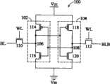
参阅图1,图1是显示具有两相互耦接反相器102及104的标准6-晶体管SRAM单元的电路图100。反相器102包括一上拉(pull-up)晶体管114及一下拉(pull-down)晶体管116。反相器104包括一上拉晶体管118及一下拉晶体管120。反相器102的中央储存节点106直接耦接至反相器104中两个晶体管的栅极。反相器104的中央储存节点108直接耦接至反相器102中两个晶体管的栅极。反相器102的中央储存节点106通过耦接至位线(bit line)BL的转换晶体管110来写入及读取。反相器104的中央储存节点108通过耦接至位线BLB的转换晶体管112来写入及读取。两个转换晶体管110及112由一共同字线(word line)WL来控制。接着,以SRAM单元为背景来解释本发明各式不同的实施例。Referring to FIG. 1 , FIG. 1 is a circuit diagram 100 showing a standard 6-transistor SRAM cell with two mutually coupled
图2是显示依照本发明一实施例的一单位存储单元的集成电路布局200,准备沉积第一金属层。该单位存储单元的边界由线202、204、206及208所界定。P+注入物掺杂于视窗210内所有接触区,N+注入物则掺杂于视窗210外所有接触区。如图所示,接触区236、238、232及234掺入P+杂质。多晶硅(polycrystallinesilicon)线220及226其接触区212及214亦掺入P+杂质。其他所有主动及多晶硅接触区则掺入N+杂质。接触区212应用于反相器的多晶硅栅极220(用以控制上拉晶体管222及下拉晶体管224)。接触区214应用于反相器的多晶硅栅极226(用以控制上拉晶体管228及下拉晶体管230)。FIG. 2 shows an integrated circuit layout 200 of a unit memory cell, ready for deposition of a first metal layer, according to an embodiment of the present invention. The boundaries of the unit cell are defined by
参照图1及图2,晶体管228是一具有接触区232及234的P-沟道金属氧化物半导体(metal oxide semiconductor;MOS)晶体管。晶体管222是一具有接触区236及238的PMOS晶体管。晶体管230是一具有接触区240及242的NMOS晶体管。晶体管224是一具有接触区244及246的NMOS晶体管。传输栅晶体管(pass-gate transistor)248是具有源极接触区250(耦接至位线BL)与漏极接触区242(与晶体管230的漏极接触区共有,且为储存节点106的一部分)的NMOS晶体管。晶体管252是具有源极接触区254(耦接至位线BLB)与漏极接触区246(与晶体管224的漏极接触区共有,且为储存节点108的一部分)的NMOS晶体管。控制晶体管248的多晶硅栅极256具有耦接至字线WL的接触区258。控制晶体管252的多晶硅栅极260具有耦接至字线WL的接触区262。Referring to FIGS. 1 and 2 , transistor 228 is a P-channel metal oxide semiconductor (MOS) transistor with
图3是显示依照本发明的一实施例的一单位存储单元的集成电路布局300,沉积有第一金属层。L-型垫片302耦接接触区212至接触区234及242以形成一储存节点SN。L-型垫片304耦接接触区214至接触区238及246以形成一储存节点SNB。垫片306耦接至接触区236。垫片308耦接至接触区232。垫片310耦接至接触区240。垫片312耦接至接触区244。垫片314耦接至接触区250。垫片316耦接至接触区254。垫片318耦接至接触区258。垫片320耦接至接触区262。FIG. 3 shows an
图4A提供一传统的集成电路内连线结构的布局400。导体层402形成于第一金属层上。接触区404(由导电材料注入介层孔而形成)建构在第一导体层402上,且耦接至第二金属层上的着陆垫片406。接触区408(由导电材料注入介层孔而形成)建构在着陆垫片406上,且耦接至第三金属层上的导体层410。FIG. 4A provides a
如上述所论,因为有限的光学微影(photolithography)技术,持续缩小的介层接触区对集成电路制造形成一大挑战。照惯例,着陆垫片406用来提供介层接触区404及408适当的着陆空间(landing margin)。然而,这使得内连线结构的制造变得复杂。因此,期望有不包括着陆垫片(即不包括介层接触区404及408的着陆空间)的内连线结构。As discussed above, the ever-shrinking via contact area poses a major challenge to IC fabrication due to limited photolithography techniques. Conventionally, landing
图4B是显示依照本发明的一实施例的内连线结构布局412。第一导体层420形成于半导体基底上(图未显示)。第一接触区414(由导电材料注入介层孔而形成)形成于第一导体层420上。第二接触区416(由导电材料注入介层孔而形成)形成于第一介层接触区414上。第二导体层418形成于第二介层接触区416上。在该实施例中,第一介层接触区414的横截面大体上大于第二介层接触区416的横截面。在另一实施例中,第一介层接触区414的横截面至少大于第二介层接触区416的横截面40%。如此改善了第一介层接触区414与第二介层接触区416之间的着陆空间(landingmargin)。因此,介层接触区414与416可直接相互耦接而无需在其间使用着陆垫片(landing pad)。FIG. 4B shows an
在该实施例中,第一介层接触区414与第二介层接触区416各有大体上与纵向方向一致的侧壁。从俯视图来看,第一介层接触区414的横截面边界大得足以围绕第二介层接触区416的横截面边界。第一介层接触区414与第二介层接触区416大体上可以铜(Cu)、氮化钽(TaN)、碳化硅(SiC)、钨(W)或氮化钛(TiN)制成。In this embodiment, each of the first via
要注意的是,虽然在该实施例中,介层接触区414与416的横截面分别为椭圆形与圆形,但亦可为其他形状。例如,半导体制造业常将其设计成矩形。It should be noted that although in this embodiment, the cross-sections of the via
要注意的是,在本发明的另一实施例中,第二介层接触区416的横截面可大体上大于第一介层接触区414的横截面,且亦提供其间改善的着陆空间(landing margin)。It should be noted that, in another embodiment of the present invention, the cross-section of the second via
图5A及图5B是显示依照本发明的不同实施例的内连线结构的横截面图516及526。图5A显示本发明的内连线结构的横截面图516,其中放大的介层接触区518与正常大小的介层接触区520相互直接耦接,以电性耦接导体层522及524。5A and 5B are
参照图5B,第一导体层528形成于第一金属层上。形成于第一金属层上的第一介层接触区532直接耦接至第一导体层528。第二介层接触区536直接耦接至第二金属层上的第二导体层530。一个以上的中间介层接触区534耦接于第一介层接触区532与第二介层接触区536之间(在一个以上的中间金属层之上,介于第一金属层与第二金属层之间)。第一介层接触区532、第二介层接触区536、以及中间介层接触区534其中之一横截面大体上大于其他的横截面,以改善着陆空间(landing margin)因而无需在其间使用着陆垫片(landing pad)。Referring to FIG. 5B, a
在该实施例中,中间介层接触区的深度延伸贯穿中间金属层,以使得第一导体层528的第一金属层与第二导体层530的第二金属层被一个以上中间金属层分隔。第一介层接触区532、第二介层接触区536、以及中间介层接触区534各有大体上与纵向方向一致的侧壁。第一介层接触区532的横截面大体上大于第二介层接触区536的横截面。从俯视图来看,第一介层接触区532的横截面边界大得足以围绕第二介层接触区536的横截面边界。中间介层接触区534的横截面大体上大于第二介层接触区536的横截面。从俯视图来看,中间介层接触区534的横截面边界大得足以围绕第二介层接触区536的横截面边界。要注意的是,在本发明的另一实施例中,第二介层接触区536与第一介层接触区532的位置可互换。In this embodiment, the depth of the interposer contact region extends through the intermediate metal layer, such that the first metal layer of the
图6是显示本发明应用至SRAM存储单元,沉积有第一金属层与第一介层孔层。单位存储单元的轮廓由线202、204、206及208勾勒出来。金属图案布局618显示依照本发明的一实施例,放大的介层接触区620、622、624及626如何形成于第一介层孔层上。FIG. 6 is a diagram showing the application of the present invention to a SRAM memory cell, where a first metal layer and a first via layer are deposited. Unit memory cells are outlined by
图7是显示本发明应用至SRAM存储单元,具有第一金属层、第一介层孔层及第二金属层。单位存储单元的轮廓由线202、204、206及208勾勒出来。金属图案布局716显示放大的介层接触区620、622、624及626。介层接触区604及612在第二金属层上被线704覆盖着。而介层接触区606在第二金属层上被线706覆盖着。第一介层孔层614在第二金属层上被线712覆盖着。FIG. 7 shows the application of the present invention to a SRAM memory cell, which has a first metal layer, a first via layer and a second metal layer. Unit memory cells are outlined by
虽然本发明已通过较佳实施例说明如上,但该较佳实施例并非用以限定本发明。本领域的技术人员,在不脱离本发明的精神和范围内,应有能力对该较佳实施例做出各种更改和补充,因此本发明的保护范围以权利要求书的范围为准。Although the present invention has been described above through preferred embodiments, the preferred embodiments are not intended to limit the present invention. Those skilled in the art should be able to make various changes and supplements to the preferred embodiment without departing from the spirit and scope of the present invention. Therefore, the scope of protection of the present invention is subject to the scope of the claims.
附图中符号的简单说明如下:A brief description of the symbols in the drawings is as follows:
100:具有标准6-晶体管SRAM单元的电路图100: Circuit diagram with a standard 6-transistor SRAM cell
102、104:反相器102, 104: Inverter
106、108:中央储存节点106, 108: central storage nodes
110、112:转换晶体管110, 112: conversion transistor
114、118、222、228:上拉(pull-up)晶体管114, 118, 222, 228: pull-up transistors
116、120、224、230:下拉(pull-down)晶体管116, 120, 224, 230: pull-down transistors
200、300:单位存储单元的集成电路布局200, 300: IC layout of unit memory cell
202、204、206、208、704、706、712:线202, 204, 206, 208, 704, 706, 712: line
210:视窗210: Windows
212、214、232、234、236、238、240、242、244、246、250、254、258、262、404、408、414、416、518、520、532、534、536、604、606、612、620、622、624、626:接触区212, 214, 232, 234, 236, 238, 240, 242, 244, 246, 250, 254, 258, 262, 404, 408, 414, 416, 518, 520, 532, 534, 536, 604, 606, 612, 620, 622, 624, 626: contact area
220、226、256、260:多晶硅栅极(多晶硅线)220, 226, 256, 260: polysilicon gate (polysilicon line)
248、252:控制晶体管248, 252: control transistor
302、304、306、308、310、312、314、316、318、320、406:垫片302, 304, 306, 308, 310, 312, 314, 316, 318, 320, 406: gasket
400、412:内连线结构布局400, 412: Internal wiring structure layout
402、410、418、420、522、524、528、530:导体层402, 410, 418, 420, 522, 524, 528, 530: conductor layer
516、526:内连线结构的横截面516, 526: Cross-section of interconnection structure
614:介层孔层614: via layer
618、716:金属图案布局618, 716: metal pattern layout
BL、BLB:位线BL, BLB: bit line
Vcc、Vss:电压Vcc, Vss: Voltage
WL:字线WL: word line
Claims (11)
Translated fromChineseApplications Claiming Priority (2)
| Application Number | Priority Date | Filing Date | Title |
|---|---|---|---|
| US11/170,369 | 2005-06-29 | ||
| US11/170,369US8405216B2 (en) | 2005-06-29 | 2005-06-29 | Interconnect structure for integrated circuits |
Publications (2)
| Publication Number | Publication Date |
|---|---|
| CN1893056A CN1893056A (en) | 2007-01-10 |
| CN100420011Ctrue CN100420011C (en) | 2008-09-17 |
Family
ID=37588472
Family Applications (1)
| Application Number | Title | Priority Date | Filing Date |
|---|---|---|---|
| CNB2006100765140AActiveCN100420011C (en) | 2005-06-29 | 2006-04-28 | Interconnect structure for integrated circuit and SRAM cell |
Country Status (3)
| Country | Link |
|---|---|
| US (1) | US8405216B2 (en) |
| CN (1) | CN100420011C (en) |
| TW (1) | TWI315559B (en) |
Families Citing this family (28)
| Publication number | Priority date | Publication date | Assignee | Title |
|---|---|---|---|---|
| US8658542B2 (en) | 2006-03-09 | 2014-02-25 | Tela Innovations, Inc. | Coarse grid design methods and structures |
| US9035359B2 (en) | 2006-03-09 | 2015-05-19 | Tela Innovations, Inc. | Semiconductor chip including region including linear-shaped conductive structures forming gate electrodes and having electrical connection areas arranged relative to inner region between transistors of different types and associated methods |
| US8448102B2 (en) | 2006-03-09 | 2013-05-21 | Tela Innovations, Inc. | Optimizing layout of irregular structures in regular layout context |
| US9563733B2 (en) | 2009-05-06 | 2017-02-07 | Tela Innovations, Inc. | Cell circuit and layout with linear finfet structures |
| US7763534B2 (en) | 2007-10-26 | 2010-07-27 | Tela Innovations, Inc. | Methods, structures and designs for self-aligning local interconnects used in integrated circuits |
| US8541879B2 (en)* | 2007-12-13 | 2013-09-24 | Tela Innovations, Inc. | Super-self-aligned contacts and method for making the same |
| US7956421B2 (en) | 2008-03-13 | 2011-06-07 | Tela Innovations, Inc. | Cross-coupled transistor layouts in restricted gate level layout architecture |
| US8839175B2 (en) | 2006-03-09 | 2014-09-16 | Tela Innovations, Inc. | Scalable meta-data objects |
| US9230910B2 (en) | 2006-03-09 | 2016-01-05 | Tela Innovations, Inc. | Oversized contacts and vias in layout defined by linearly constrained topology |
| US8653857B2 (en) | 2006-03-09 | 2014-02-18 | Tela Innovations, Inc. | Circuitry and layouts for XOR and XNOR logic |
| US7446352B2 (en) | 2006-03-09 | 2008-11-04 | Tela Innovations, Inc. | Dynamic array architecture |
| US9009641B2 (en) | 2006-03-09 | 2015-04-14 | Tela Innovations, Inc. | Circuits with linear finfet structures |
| US8667443B2 (en)* | 2007-03-05 | 2014-03-04 | Tela Innovations, Inc. | Integrated circuit cell library for multiple patterning |
| US7888705B2 (en)* | 2007-08-02 | 2011-02-15 | Tela Innovations, Inc. | Methods for defining dynamic array section with manufacturing assurance halo and apparatus implementing the same |
| US8453094B2 (en) | 2008-01-31 | 2013-05-28 | Tela Innovations, Inc. | Enforcement of semiconductor structure regularity for localized transistors and interconnect |
| US7939443B2 (en) | 2008-03-27 | 2011-05-10 | Tela Innovations, Inc. | Methods for multi-wire routing and apparatus implementing same |
| SG192532A1 (en) | 2008-07-16 | 2013-08-30 | Tela Innovations Inc | Methods for cell phasing and placement in dynamic array architecture and implementation of the same |
| US9122832B2 (en)* | 2008-08-01 | 2015-09-01 | Tela Innovations, Inc. | Methods for controlling microloading variation in semiconductor wafer layout and fabrication |
| US8661392B2 (en)* | 2009-10-13 | 2014-02-25 | Tela Innovations, Inc. | Methods for cell boundary encroachment and layouts implementing the Same |
| US8399931B2 (en) | 2010-06-30 | 2013-03-19 | Taiwan Semiconductor Manufacturing Company, Ltd. | Layout for multiple-fin SRAM cell |
| US8675397B2 (en) | 2010-06-25 | 2014-03-18 | Taiwan Semiconductor Manufacturing Company, Ltd. | Cell structure for dual-port SRAM |
| KR101732645B1 (en) | 2010-04-06 | 2017-05-08 | 삼성전자주식회사 | Semiconductor device including sram cell and methods of fabricating the same |
| US9159627B2 (en) | 2010-11-12 | 2015-10-13 | Tela Innovations, Inc. | Methods for linewidth modification and apparatus implementing the same |
| US9122830B2 (en)* | 2013-06-03 | 2015-09-01 | Globalfoundries Inc. | Wide pin for improved circuit routing |
| KR102088200B1 (en) | 2014-07-01 | 2020-03-13 | 삼성전자주식회사 | Semiconductor device and method of manufacturing the same |
| US10147682B2 (en)* | 2015-11-30 | 2018-12-04 | Taiwan Semiconductor Manufacturing Co., Ltd. | Structure for stacked logic performance improvement |
| US10211206B1 (en)* | 2017-11-01 | 2019-02-19 | Globalfoundries Inc. | Two-port vertical SRAM circuit structure and method for producing the same |
| US10727237B2 (en)* | 2018-09-27 | 2020-07-28 | Taiwan Semiconductor Manufacturing Co., Ltd. | Semiconductor structure |
Citations (5)
| Publication number | Priority date | Publication date | Assignee | Title |
|---|---|---|---|---|
| CN1224243A (en)* | 1997-12-23 | 1999-07-28 | 三星电子株式会社 | CMOS static random access memory devices |
| US6080664A (en)* | 1998-05-29 | 2000-06-27 | Vanguard International Semiconductor Corporation | Method for fabricating a high aspect ratio stacked contact hole |
| CN1281257A (en)* | 1999-06-28 | 2001-01-24 | 株式会社东芝 | Semiconductor device |
| US6649517B2 (en)* | 2001-05-18 | 2003-11-18 | Chartered Semiconductor Manufacturing Ltd. | Copper metal structure for the reduction of intra-metal capacitance |
| US6882576B2 (en)* | 2003-01-16 | 2005-04-19 | Renesas Technology Corp. | Semiconductor memory device |
Family Cites Families (42)
| Publication number | Priority date | Publication date | Assignee | Title |
|---|---|---|---|---|
| US5378927A (en)* | 1993-05-24 | 1995-01-03 | International Business Machines Corporation | Thin-film wiring layout for a non-planar thin-film structure |
| KR100375428B1 (en)* | 1995-11-20 | 2003-05-17 | 가부시끼가이샤 히다치 세이사꾸쇼 | Semiconductor storage device and process for manufacturing the same |
| FR2754391B1 (en)* | 1996-10-08 | 1999-04-16 | Sgs Thomson Microelectronics | HIGH SHAPE FACTOR CONTACT STRUCTURE FOR INTEGRATED CIRCUITS |
| JPH10135425A (en)* | 1996-11-05 | 1998-05-22 | Hitachi Ltd | Semiconductor integrated circuit device and method of manufacturing the same |
| JP3523762B2 (en)* | 1996-12-19 | 2004-04-26 | 株式会社東芝 | Semiconductor storage device |
| US6121129A (en)* | 1997-01-15 | 2000-09-19 | International Business Machines Corporation | Method of contact structure formation |
| JPH10242147A (en)* | 1997-02-27 | 1998-09-11 | Toshiba Corp | Semiconductor device and method of manufacturing the same, semiconductor memory device and method of manufacturing the same |
| JP3599548B2 (en)* | 1997-12-18 | 2004-12-08 | 株式会社日立製作所 | Method for manufacturing semiconductor integrated circuit device |
| US20020070453A1 (en)* | 1998-11-17 | 2002-06-13 | Koji Yamamoto | Semiconductor device and method of producing thereof |
| JP2000183313A (en)* | 1998-12-21 | 2000-06-30 | Hitachi Ltd | Semiconductor integrated circuit device and method of manufacturing the same |
| US6277761B1 (en)* | 1999-01-20 | 2001-08-21 | Siemens Aktiengesellschaft | Method for fabricating stacked vias |
| JP4565700B2 (en)* | 1999-05-12 | 2010-10-20 | ルネサスエレクトロニクス株式会社 | Semiconductor device |
| US6127260A (en)* | 1999-07-16 | 2000-10-03 | Taiwan Semiconductor Manufacturing Company | Method of forming a tee shaped tungsten plug structure to avoid high aspect ratio contact holes in embedded DRAM devices |
| TW444395B (en)* | 1999-07-27 | 2001-07-01 | Taiwan Semiconductor Mfg | Processing method to planarize the crown capacitor device |
| JP3915861B2 (en)* | 2000-01-14 | 2007-05-16 | セイコーエプソン株式会社 | Semiconductor device and manufacturing method thereof |
| US6274409B1 (en)* | 2000-01-18 | 2001-08-14 | Agere Systems Guardian Corp. | Method for making a semiconductor device |
| US7087493B1 (en)* | 2000-08-09 | 2006-08-08 | Texas Instruments Incorporated | Memory with 6T small aspect ratio cells having metal—1 elements physically connected to metal—0 elements |
| JP2002343861A (en)* | 2001-05-21 | 2002-11-29 | Mitsubishi Electric Corp | Semiconductor integrated circuit and method of manufacturing the same |
| JP4911838B2 (en)* | 2001-07-06 | 2012-04-04 | ルネサスエレクトロニクス株式会社 | Semiconductor device and manufacturing method thereof |
| US6810583B2 (en)* | 2001-08-07 | 2004-11-02 | International Business Machines Corporation | Coupling of conductive vias to complex power-signal substructures |
| US6734477B2 (en)* | 2001-08-08 | 2004-05-11 | Agilent Technologies, Inc. | Fabricating an embedded ferroelectric memory cell |
| JP3637299B2 (en)* | 2001-10-05 | 2005-04-13 | 松下電器産業株式会社 | Semiconductor memory device |
| US6737685B2 (en)* | 2002-01-11 | 2004-05-18 | International Business Machines Corporation | Compact SRAM cell layout for implementing one-port or two-port operation |
| AU2003223386A1 (en)* | 2002-03-27 | 2003-10-13 | The Regents Of The University Of California | Low-power high-performance memory cell and related methods |
| KR100502410B1 (en)* | 2002-07-08 | 2005-07-19 | 삼성전자주식회사 | DRAM cells |
| JP2004096065A (en)* | 2002-07-08 | 2004-03-25 | Renesas Technology Corp | Semiconductor memory device and method of manufacturing the same |
| JP4037711B2 (en)* | 2002-07-26 | 2008-01-23 | 株式会社東芝 | Semiconductor device having a capacitor formed in an interlayer insulating film |
| JP4343571B2 (en)* | 2002-07-31 | 2009-10-14 | 株式会社ルネサステクノロジ | Manufacturing method of semiconductor device |
| JP2004079696A (en)* | 2002-08-14 | 2004-03-11 | Renesas Technology Corp | Semiconductor storage device |
| US7084509B2 (en)* | 2002-10-03 | 2006-08-01 | International Business Machines Corporation | Electronic package with filled blinds vias |
| US6972209B2 (en)* | 2002-11-27 | 2005-12-06 | International Business Machines Corporation | Stacked via-stud with improved reliability in copper metallurgy |
| JP2004253730A (en)* | 2003-02-21 | 2004-09-09 | Renesas Technology Corp | Semiconductor integrated circuit device and its manufacturing method |
| JP2004296998A (en)* | 2003-03-28 | 2004-10-21 | Matsushita Electric Ind Co Ltd | Semiconductor device |
| JP2004363256A (en)* | 2003-06-03 | 2004-12-24 | Nec Electronics Corp | Semiconductor device and method for manufacturing the same |
| JP2004363214A (en)* | 2003-06-03 | 2004-12-24 | Renesas Technology Corp | Method of manufacturing semiconductor integrated circuit device and semiconductor integrated circuit device |
| JP2005032991A (en)* | 2003-07-14 | 2005-02-03 | Renesas Technology Corp | Semiconductor device |
| US7319065B1 (en)* | 2003-08-08 | 2008-01-15 | Advanced Micro Devices, Inc. | Semiconductor component and method of manufacture |
| JP4606006B2 (en)* | 2003-09-11 | 2011-01-05 | ルネサスエレクトロニクス株式会社 | Manufacturing method of semiconductor device |
| US7067902B2 (en)* | 2003-12-02 | 2006-06-27 | International Business Machines Corporation | Building metal pillars in a chip for structure support |
| US7221034B2 (en)* | 2004-02-27 | 2007-05-22 | Infineon Technologies Ag | Semiconductor structure including vias |
| US7378342B2 (en)* | 2004-08-27 | 2008-05-27 | Micron Technology, Inc. | Methods for forming vias varying lateral dimensions |
| US20060289202A1 (en)* | 2005-06-24 | 2006-12-28 | Intel Corporation | Stacked microvias and method of manufacturing same |
- 2005
- 2005-06-29USUS11/170,369patent/US8405216B2/enactiveActive
- 2006
- 2006-04-06TWTW095112111Apatent/TWI315559B/enactive
- 2006-04-28CNCNB2006100765140Apatent/CN100420011C/enactiveActive
Patent Citations (5)
| Publication number | Priority date | Publication date | Assignee | Title |
|---|---|---|---|---|
| CN1224243A (en)* | 1997-12-23 | 1999-07-28 | 三星电子株式会社 | CMOS static random access memory devices |
| US6080664A (en)* | 1998-05-29 | 2000-06-27 | Vanguard International Semiconductor Corporation | Method for fabricating a high aspect ratio stacked contact hole |
| CN1281257A (en)* | 1999-06-28 | 2001-01-24 | 株式会社东芝 | Semiconductor device |
| US6649517B2 (en)* | 2001-05-18 | 2003-11-18 | Chartered Semiconductor Manufacturing Ltd. | Copper metal structure for the reduction of intra-metal capacitance |
| US6882576B2 (en)* | 2003-01-16 | 2005-04-19 | Renesas Technology Corp. | Semiconductor memory device |
Also Published As
| Publication number | Publication date |
|---|---|
| US20070001304A1 (en) | 2007-01-04 |
| CN1893056A (en) | 2007-01-10 |
| TWI315559B (en) | 2009-10-01 |
| TW200701398A (en) | 2007-01-01 |
| US8405216B2 (en) | 2013-03-26 |
Similar Documents
| Publication | Publication Date | Title |
|---|---|---|
| CN100420011C (en) | Interconnect structure for integrated circuit and SRAM cell | |
| USRE49203E1 (en) | Layout for multiple-fin SRAM cell | |
| US11063053B2 (en) | Integrated circuit and static random access memory thereof | |
| US10163495B2 (en) | Two-port SRAM connection structure | |
| US11145660B2 (en) | Dual-port SRAM cell structure | |
| JP4044721B2 (en) | Manufacturing method of semiconductor integrated circuit device | |
| CN100470833C (en) | Semiconductor structure and forming method thereof | |
| KR100474602B1 (en) | Semiconductor memory device | |
| CN111106115B (en) | Semiconductor structure | |
| US9196352B2 (en) | Static random access memory unit cell structure and static random access memory unit cell layout structure | |
| US7410843B2 (en) | Methods for fabricating reduced floating body effect static random access memory cells | |
| US10727237B2 (en) | Semiconductor structure | |
| EP4057154A1 (en) | Integrated scaling and stretching platform for optimizing monolithic integration and/or heterogeneous integration in a single semiconductor die | |
| US11569218B2 (en) | Semiconductor integrated circuit device | |
| US20230240087A1 (en) | Integrated scaling and stretching platform for server processor and rack server unit | |
| JP2025102809A (en) | Homogeneous/heterogeneous integrated systems with high performance computing and high storage capacity | |
| TWI843480B (en) | Sram cell | |
| JP2006140490A (en) | Semiconductor chip | |
| JP2022140348A5 (en) | ||
| CN220858819U (en) | Semiconductor devices | |
| US6713886B2 (en) | Semiconductor device | |
| CN120282442A (en) | Semiconductor device and semiconductor structure | |
| JP2010073914A (en) | Semiconductor device and method of manufacturing the same |
Legal Events
| Date | Code | Title | Description |
|---|---|---|---|
| C06 | Publication | ||
| PB01 | Publication | ||
| C10 | Entry into substantive examination | ||
| SE01 | Entry into force of request for substantive examination | ||
| C14 | Grant of patent or utility model | ||
| GR01 | Patent grant |