CN100419835C - Pixel circuit and display device - Google Patents
Pixel circuit and display deviceDownload PDFInfo
- Publication number
- CN100419835C CN100419835CCNB2004800323727ACN200480032372ACN100419835CCN 100419835 CCN100419835 CCN 100419835CCN B2004800323727 ACNB2004800323727 ACN B2004800323727ACN 200480032372 ACN200480032372 ACN 200480032372ACN 100419835 CCN100419835 CCN 100419835C
- Authority
- CN
- China
- Prior art keywords
- tft
- voltage
- correction
- driving transistors
- transistor
- Prior art date
- Legal status (The legal status is an assumption and is not a legal conclusion. Google has not performed a legal analysis and makes no representation as to the accuracy of the status listed.)
- Expired - Lifetime
Links
Images


Landscapes
- Control Of Indicators Other Than Cathode Ray Tubes (AREA)
Abstract
Description
Translated fromChinese技术领域technical field
本发明关于包含有机EL(Electro Luminescence:电场发光)组件等发光组件的像素电路、及将该有机EL组件配置成矩阵状的显示装置。The present invention relates to a pixel circuit including a light-emitting element such as an organic EL (Electro Luminescence) element, and a display device in which the organic EL element is arranged in a matrix.
背景技术Background technique
已知有使用有机EL组件作为发光组件的有机EL面板,且其开发也有所进展。在该有机EL面板中,将有机EL组件配置成矩阵状,个别控制该有机EL组件的发光,而执行显示。尤其在主动矩阵式有机EL面板中,每个像素都具有控制显示用的TFT,由此控制该TFT的动作,便可控制每个像素的发光,所以可以执行精度非常高的显示。An organic EL panel using an organic EL element as a light-emitting element is known, and its development is progressing. In this organic EL panel, organic EL elements are arranged in a matrix, and light emission of the organic EL elements is individually controlled to perform display. In particular, in an active matrix organic EL panel, each pixel has a TFT for controlling display, and by controlling the operation of the TFT, the light emission of each pixel can be controlled, so that very high-precision display can be performed.
图13所表示的是主动矩阵式有机EL面板的像素电路的一例。供应显示像素亮度的数据电压的数据线经由栅极连接于栅极线的n沟道的选择TFT 10,而连接于驱动TFT 12的栅极。此外,在驱动TFT 12的栅极连接有另一端连接于保持电容线SC的保持电容14的一端,并保持驱动TFT 12的栅极电压。FIG. 13 shows an example of a pixel circuit of an active matrix organic EL panel. A data line supplying a data voltage for displaying pixel luminance is connected to a gate of a driving
驱动TFT 12的源极连接于EL电源线,漏极连接于有机EL组件16的阳极,有机EL组件16的阴极连接于阴极电源。The source of the driving TFT 12 is connected to the EL power supply line, the drain is connected to the anode of the
这种像素电路被配置成矩阵状,依预定时序(timing)使设置于每个水平线的栅极线变成H电位,该行的选择TFT 10成为导通(ON)状态。在此状态下,为能对数据线依序供应数据电压,该数据电压被供应并保持于保持电容14,即便栅极线转变为L电位,仍保持该时的电压。Such pixel circuits are arranged in a matrix, and the gate lines provided on each horizontal line are set at H potential at predetermined timing, so that the
然后,对应此保持电容14中所保持的电压,使驱动TFT 12产生动作,相对应的驱动电流从EL电源线经由有机EL组件16而流入阴极电源,有机EL组件16便对应数据电压而进行发光。Then, corresponding to the voltage held in the
然后,将栅极线依序转为H电位,将所输入的视频信号(video signal)当作数据电压依序供应给所对应的像素,借此被配置成矩阵状的有机EL组件16便对应数据电压进行发光,执行关于视频信号的显示。Then, the gate lines are sequentially turned to H potential, and the input video signal (video signal) is sequentially supplied to the corresponding pixels as a data voltage, so that the
但是,在此种像素电路中,配置成矩阵状的像素电路的驱动TFT,若其临限值电压不均匀的话,亮度将呈不均匀状态,而造成显示质量降低的问题发生。所以,针对构成整个显示面板的像素电路的TFT,难以将其特性变为相同状态,且难以防止其导通或关断的临限值不发生不均现象。However, in such a pixel circuit, if the threshold voltages of the drive TFTs arranged in a matrix are not uniform, the luminance will be non-uniform, resulting in a problem of degradation in display quality. Therefore, it is difficult to make the characteristics of the TFTs constituting the pixel circuits of the entire display panel into the same state, and it is difficult to prevent non-uniformity in the threshold value of their turn-on or turn-off.
所以,便期待防止驱动TFT的临限值不均对于显示造成影响。Therefore, it is desired to prevent the non-uniform threshold value of the driving TFT from affecting the display.
在此,针对用以防止对TFT临限值变动造成影响的电路,自以往便有各种方案(例如日本专利特表2002-514320号公报)。Here, conventionally, there have been various proposals for circuits for preventing the influence of fluctuations in the TFT threshold value (for example, Japanese Patent Laid-Open No. 2002-514320).
但是,在该方案中,需要设置用以进行临限值变动补偿的电路。所以,若使用这种电路的话,便会发生像素电路的组件数增加,开口率变小的问题发生。此外,当追加补偿用的电路时,将产生驱动像素电路用的外围电路必须变更的问题。However, in this scheme, it is necessary to provide a circuit for compensating for fluctuations in the threshold value. Therefore, if such a circuit is used, the number of components of the pixel circuit increases and the aperture ratio becomes smaller. In addition, when a circuit for compensation is added, there arises a problem that peripheral circuits for driving pixel circuits must be changed.
发明内容Contents of the invention
本发明提供一种以简单的变更,便可有效的补偿驱动晶体管的临限值电压变动的像素电路。The invention provides a pixel circuit capable of effectively compensating the variation of the threshold voltage of the driving transistor by simple modification.
本发明所涉及的一种像素电路,其具有:一端连接于数据线,且对控制端输入选择信号的选择晶体管;一端连接于此选择晶体管的另一端,且控制端连接于预定电压的第1电源的修正晶体管;控制端连接于此修正晶体管的另一端,一端连接于作为电流供应源的第2电源的驱动晶体管;一端连接于此驱动晶体管的控制端,另一端连接于脉冲电压线的保持电容;以及利用流通于所述驱动晶体管的电流而发光的发光组件;在利用变更所述脉冲电压线的电压值而导通所述驱动晶体管的过程中,使所述修正晶体管导通或关断,借此控制驱动晶体管导通时的控制端电压,同时所述驱动晶体管与所述修正晶体管形成邻接状态。A pixel circuit according to the present invention includes: a selection transistor whose one end is connected to a data line and a selection signal is input to a control end; The correction transistor of the power supply; the control end is connected to the other end of the correction transistor, and one end is connected to the drive transistor of the second power supply as the current supply source; one end is connected to the control end of the drive transistor, and the other end is connected to the hold of the pulse voltage line a capacitor; and a light-emitting element that emits light by using the current flowing through the driving transistor; during the process of turning on the driving transistor by changing the voltage value of the pulse voltage line, the correction transistor is turned on or off , so as to control the voltage of the control terminal when the driving transistor is turned on, and at the same time, the driving transistor and the correction transistor form an adjacent state.
再者,优选的是,所述数据线与电源线朝垂直扫描方向延伸,且所述修正晶体管形成于所述数据线与电源线之间。Furthermore, preferably, the data line and the power line extend in a vertical scanning direction, and the correction transistor is formed between the data line and the power line.
再者,所述驱动晶体管优选的是,夹着所述电源线,而形成于所述修正晶体管的相反侧。Furthermore, it is preferable that the drive transistor is formed on the opposite side of the correction transistor across the power supply line.
再者,优选的是,在将所述选择晶体管导通的状态下,对数据线供应使修正晶体管导通的数据电压,并将对应数据电压的电压保持在驱动晶体管的控制端,然后,使所述选择晶体管关断,在此状态下,使脉冲电压线的电压产生变化,且使驱动晶体管的控制端电压移位,借此使修正晶体管关断,同时使驱动晶体管导通,且使对应数据电压的电流流通于驱动晶体管。Furthermore, preferably, in the state where the selection transistor is turned on, the data line is supplied with a data voltage for turning on the correction transistor, and the voltage corresponding to the data voltage is kept at the control terminal of the driving transistor, and then, the The selection transistor is turned off. In this state, the voltage of the pulse voltage line is changed, and the voltage of the control terminal of the driving transistor is shifted, so that the correction transistor is turned off, and the driving transistor is turned on at the same time, and the corresponding The current of the data voltage flows through the driving transistor.
再者,优选的是,所述第1电源与第2电源为同一电源。Furthermore, preferably, the first power supply and the second power supply are the same power supply.
再者,所述修正晶体管与驱动晶体管是p型沟道晶体管,优选的是,所述脉冲电压线在所述选择晶体管关断之后,从高电位变化成低电位。Furthermore, the correction transistor and the driving transistor are p-type channel transistors. Preferably, the pulse voltage line changes from a high potential to a low potential after the selection transistor is turned off.
本发明的另一实施例涉及若干若干个像素排列成矩阵状的显示装置,各像素具有:对应供应电力进行动作的显示组件;第1导电区域连接于数据线,并对控制端输入选择信号的选择晶体管;第1导电区域连接于电源线,将电力供应给所述显示组件的驱动晶体管;控制端连接于预定电压的第1电源,第1导电区域连接于所述选择晶体管的第2导电区域,第2导电区域连接于所述驱动晶体管的控制端的修正晶体管;以及,第1电极连接于所述驱动晶体管的控制端与所述修正晶体管的第2导电区域,第2电极连接于脉冲电压线的保持电容。此外,所述驱动晶体管的控制端电压对应所述脉冲电压线的电压变动产生变化,而对应于此变化,所述修正晶体管对应其动作临限值来控制所述驱动晶体管成为导通状态时的所述控制端电压。另外,所述修正晶体管与所述驱动晶体管由同一导电型晶体管所构成,且所述修正晶体管与所述驱动晶体管的至少沟道区域,均由经激光退火而多结晶化的半导体层所构成,该沟道区域相互接近配置。Another embodiment of the present invention relates to a display device in which a plurality of pixels are arranged in a matrix, and each pixel has: a display component that operates corresponding to the power supply; the first conductive region is connected to the data line, and a selection signal is input to the control terminal Selection transistor; the first conductive area is connected to the power line, and power is supplied to the driving transistor of the display component; the control terminal is connected to the first power supply of a predetermined voltage, and the first conductive area is connected to the second conductive area of the selection transistor , the second conductive region is connected to the correction transistor of the control terminal of the driving transistor; and the first electrode is connected to the control terminal of the driving transistor and the second conductive region of the correction transistor, and the second electrode is connected to the pulse voltage line of hold capacitance. In addition, the control terminal voltage of the driving transistor changes in response to the voltage variation of the pulse voltage line, and corresponding to this change, the correction transistor controls the voltage when the driving transistor is turned on according to its operating threshold value. the control terminal voltage. In addition, the correction transistor and the drive transistor are composed of transistors of the same conductivity type, and at least channel regions of the correction transistor and the drive transistor are composed of semiconductor layers that have been polycrystallized by laser annealing, The channel regions are arranged close to each other.
本发明的另一实施例在所述像素电路与显示装置中,所述修正晶体管的沟道长度方向与所述驱动晶体管的沟道长度方向,配置成平行于所述多结晶化激光退火时所照射的线状脉冲激光的扫描方向,且所述修正晶体管的沟道区域与所述驱动晶体管的沟道区域,其至少一部分均位于所述脉冲激光扫描方向正交方向所拉出的同一条线上。In another embodiment of the present invention, in the pixel circuit and the display device, the channel length direction of the correction transistor and the channel length direction of the driving transistor are arranged parallel to the polycrystallization laser annealing. The scanning direction of the irradiated linear pulsed laser, and at least a part of the channel region of the correction transistor and the channel region of the driving transistor are located on the same line drawn in the direction perpendicular to the pulsed laser scanning direction superior.
在本发明另一实施例所涉及的显示装置中,所述修正晶体管与所述驱动晶体管由同一导电型晶体管所构成,且采用所述修正晶体管的主动层的至少一部分在层间夹介着绝缘层而形成在所述电源线下层位置的构造。In the display device according to another embodiment of the present invention, the correction transistor and the drive transistor are composed of transistors of the same conductivity type, and at least a part of the active layer of the correction transistor is used to interpose an insulating layer between the layers. layer to form a structure at the position of the lower layer of the power cord.
再者,本发明中,在所述显示装置中,所述第1电源兼用作电源线,也可以在所述修正晶体管的主动层与所述电源线的层间形成有连接于所述电源线的所述修正晶体管的控制端。此外,所述修正晶体管也可具备有在所述数据线与所述电源线的线间,形成至少与其中一方的线呈部分重叠状态延伸的主动层。Moreover, in the present invention, in the display device, the first power supply is also used as a power supply line, and a layer connected to the power supply line may also be formed between the active layer of the correction transistor and the power supply line. The control terminal of the correction transistor. In addition, the correction transistor may include an active layer formed between the data line and the power supply line and extending in a state of partially overlapping at least one of the lines.
本发明的另一实施例在所述显示装置中,所述修正晶体管的沟道区域具备有在其沟道长度方向,沟道宽度互异的部分。According to another embodiment of the present invention, in the display device, the channel region of the correction transistor has portions having different channel widths in the channel length direction.
如以上所述,根据本发明,在利用变更脉冲电压线的电压值而使驱动晶体管导通的过程中,变更修正晶体管的导通或关断状态,借此来控制驱动晶体管导通时的控制端电压。所以,可对应修正晶体管的临限值电压,将不同电压设定在所对应的驱动晶体管的控制端。此外,因为将驱动晶体管与修正晶体管形成邻接状态,因而可轻易将驱动晶体管与修正晶体管的临限值电压设为相同电压,而可利用修正晶体管补偿驱动晶体管的临限值电压,且可使流通于发光组件的电流量呈均匀状态。As described above, according to the present invention, during the process of turning on the driving transistor by changing the voltage value of the pulse voltage line, the on or off state of the correction transistor is changed, thereby controlling the control when the driving transistor is turned on. terminal voltage. Therefore, different voltages can be set at the corresponding control terminals of the driving transistors corresponding to the threshold voltages of the correction transistors. In addition, since the drive transistor and the correction transistor are formed adjacent to each other, the threshold voltage of the drive transistor and the correction transistor can be easily set to the same voltage, and the threshold voltage of the drive transistor can be compensated by the correction transistor, and the current flow can be made The amount of current in the light-emitting component is uniform.
再者,数据线与电源线朝垂直扫描方向延伸,并将修正晶体管形成于数据线与电源线的线间,且夹介着电源线而在修正晶体管的相反侧形成驱动晶体管等,借此可有效率的配置,而可尽可能的增大发光组件等显示组件,而实现高开口率的显示装置。Furthermore, the data line and the power line extend in the vertical scanning direction, and the correction transistor is formed between the data line and the power line, and the driving transistor is formed on the opposite side of the correction transistor with the power line interposed therebetween, thereby enabling With efficient configuration, the display components such as light-emitting components can be enlarged as much as possible, so as to realize a display device with a high aperture ratio.
例如,在电源线的下层区域,在层间夹介着绝缘层而重叠配置修正晶体管的主动层,借此可更加提升1像素内的配置自由度。此外,当将修正晶体管的控制端(栅极电极)连接于电源线时,即便修正晶体管的主动层位于电源线下方,因为仍可对其沟道区域利用控制端来施加与电源线相同的电压,所以可减小对晶体管动作的影响。For example, in the region of the lower layer of the power supply line, the active layer of the correction transistor is overlapped with an insulating layer interposed between the layers, thereby further increasing the degree of freedom of arrangement within one pixel. In addition, when the control terminal (gate electrode) of the correction transistor is connected to the power supply line, even if the active layer of the correction transistor is located below the power supply line, the same voltage as the power supply line can still be applied to the channel region by using the control terminal , so the influence on the operation of the transistor can be reduced.
再者,在修正晶体管的沟道长度方向,设置沟道宽度互异的部分,借此也可提升1像素内的各晶体管等的配置自由度。Furthermore, in the direction of the channel length of the correction transistor, a portion having a different channel width is provided, whereby the degree of freedom in the arrangement of each transistor etc. in one pixel can also be improved.
再者,由于脉冲电压线的电压变动,驱动晶体管从关断转为导通状态,且修正晶体管的导通或关断状态切换,其电容值将产生变化。所以,因应修正晶体管的临限值变化,驱动晶体管的栅极电压便变化着利用某电压来施行修正晶体管的导通或关断的切换。此外,对应脉冲电压线变化的驱动晶体管的栅极电压的变化,乃是由修正晶体管的电容值所引起的,因此对应修正晶体管的临限值变动,栅极电压将产生变动。所以,由于以抵消驱动晶体管的临限值变动的方式,使驱动晶体管的栅极电压产生变化,因此可以尽可能整合修正晶体管的特性与驱动晶体管的特性而使控制变为容易。Furthermore, due to the voltage variation of the pulse voltage line, the driving transistor turns from off to on, and the correction transistor switches from on to off, and its capacitance value will change. Therefore, in response to the change of the threshold value of the correction transistor, the gate voltage of the drive transistor is changed to use a certain voltage to switch the correction transistor on or off. In addition, the variation of the gate voltage of the driving transistor corresponding to the variation of the pulse voltage line is caused by the capacitance value of the correction transistor, so corresponding to the variation of the threshold value of the correction transistor, the gate voltage will fluctuate. Therefore, since the gate voltage of the driving transistor is varied in such a way as to cancel out the variation of the threshold value of the driving transistor, the characteristics of the correction transistor and the characteristics of the driving transistor can be integrated as much as possible to facilitate control.
所以,当修正晶体管与驱动晶体管的沟道区域,均由经激光退火而多结晶化的半导体层所构成时,至少将此沟道区域相互接近配置,借此可轻易整合特性。Therefore, when the channel regions of the trimming transistor and the driving transistor are both composed of semiconductor layers that have been polycrystallized by laser annealing, at least the channel regions are arranged close to each other, so that characteristics can be easily integrated.
例如,当采用经激光退火而多结晶化的主动层时,将修正晶体管的沟道长度方向与驱动晶体管的沟道长度方向,配置成平行于多结晶化激光退火时所照射线状脉冲激光扫描方向,借此可对晶体管的电移动度影响较大的沟道长度方向,照射若干次的激光脉冲,可降低每个像素的各晶体管特性偏差量。此外,通过将修正晶体管的沟道区域与所述驱动晶体管的沟道区域的位置,均排列成至少一部分位于所述脉冲激光扫描方向的正交方向所拉出的同一条线上,即可因为同一激光束照射此2个晶体管的沟道区域,而使其特性更加接近。For example, when using an active layer polycrystallized by laser annealing, the channel length direction of the correction transistor and the channel length direction of the driving transistor are arranged parallel to the linear pulse laser scanning irradiated during polycrystallization laser annealing. In this way, the channel length direction, which has a greater influence on the electric mobility of the transistor, can be irradiated several times with laser pulses, which can reduce the deviation of each transistor characteristic of each pixel. In addition, by arranging the positions of the channel region of the correction transistor and the channel region of the driving transistor so that at least part of them are located on the same line drawn in the direction perpendicular to the scanning direction of the pulsed laser, it is possible because Irradiating the channel regions of these two transistors with the same laser beam brings their characteristics closer together.
再者,若所述第1电源与第2电源设为同一电源的话,便不需要个别设置电源线。Furthermore, if the first power supply and the second power supply are the same power supply, there is no need to separately install a power supply line.
再者,当将修正晶体管与驱动晶体管设定为同一p型沟道晶体管时,所述脉冲电压线在所述选择晶体管关断之后,由从高电位变化成低电位,便可有效的利用p型沟道晶体管的栅极电容。Furthermore, when the correction transistor and the driving transistor are set as the same p-channel transistor, the pulse voltage line changes from a high potential to a low potential after the selection transistor is turned off, so that the p-channel can be effectively used. type channel transistor gate capacitance.
附图说明Description of drawings
图1是本发明实施例所涉及的像素电路构造图。FIG. 1 is a structural diagram of a pixel circuit involved in an embodiment of the present invention.
图2是本发明实施例中,对栅极线GL、电容线SC所施加信号的时序图。FIG. 2 is a timing diagram of signals applied to the gate line GL and the capacitor line SC in the embodiment of the present invention.
图3是本发明实施例所涉及的栅极电压Vg24变化状态图。FIG. 3 is a diagram showing the variation state of the gate voltage Vg24 involved in the embodiment of the present invention.
图4是本发明实施例所涉及的像素电路中,所存在电容的说明图。FIG. 4 is an explanatory diagram of capacitors existing in the pixel circuit according to the embodiment of the present invention.
图5是本发明实施例所涉及的像素平面构造一例图。FIG. 5 is an example diagram of a pixel plane structure involved in an embodiment of the present invention.
图6A是沿图5A-A线的概略剖视构造图。Fig. 6A is a schematic cross-sectional structural diagram along line A-A of Fig. 5 .
图6B是沿图5B-B线的概略剖视构造图。FIG. 6B is a schematic cross-sectional structural diagram along line B-B in FIG. 5 .
图7是本发明实施例中,将修正TFT多栅极化时,平均每1像素的等效电路图。FIG. 7 is an equivalent circuit diagram per one pixel when the correction TFT is multi-gated in an embodiment of the present invention.
图8是实现图7所示等效电路的布局一例概略平面图。Fig. 8 is a schematic plan view showing an example of a layout for realizing the equivalent circuit shown in Fig. 7 .
图9是本发明实施例中,将选择TFT与修正TFT二者施行多栅极化时的等效电路图。FIG. 9 is an equivalent circuit diagram when multiple gates are performed on both the selection TFT and the correction TFT in the embodiment of the present invention.
图10是实现图9所示等效电路的布局一例图。FIG. 10 is a diagram showing an example of a layout for realizing the equivalent circuit shown in FIG. 9 .
图11是图10所示布局的另一例图。FIG. 11 is another example of the layout shown in FIG. 10 .
图12是本发明实施例的另一例电路构造图。Fig. 12 is another circuit configuration diagram of the embodiment of the present invention.
图13是已知像素电路构造图。FIG. 13 is a structural diagram of a known pixel circuit.
符号说明Symbol Description
10选择TFT 12驱动TFT10
14保持电容 16有机EL组件14 holding
20选择TFT 22修正TFT20
24驱动TFT 26有机EL组件24
28保持电容 30抑制漏电流TFT28
100透明(绝缘)基板 102缓冲层100 transparent (insulating)
104栅极绝缘膜(层) 106层间绝缘膜(层)104 gate insulating film (layer) 106 interlayer insulating film (layer)
108平面化绝缘层 110第2平面化绝缘层108
120半导体层 122主动层120
124半导体层 262第1电极(阳极)124
264第2电极(阴极) 270发光组件层264 Second electrode (cathode) 270 Light emitting component layer
272空穴输送层 274发光层272
276电子输送层 22-1第1修TFT276 Electron transport layer 22-1 1st Repair TFT
22-2第2修TFT 20c沟道区域22-2
20d漏极区域 20g(20g1、20g2)栅极电极
20s源极区域 22c沟道区域20s source
22d漏极区域 22g(22g1、22g2)栅极电极
22s源极区域 24c沟道区域22s source
24d漏极区域 24e连接电极
24g栅极 24s源极区域
24w金属配线 28e电容电极(第1电极)
Cs保持电容值 CV阴极电源Cs hold capacitor value CV cathode power supply
Cw1寄生电容 Cw2寄生电容Cw1 parasitic capacitance Cw2 parasitic capacitance
DL数据线 GL栅极线DL data line GL gate line
PL电源线 SC电容线PL power line SC capacitor line
具体实施方式Detailed ways
以下,针对本发明实施例,参照附图进行说明。Hereinafter, embodiments of the present invention will be described with reference to the drawings.
图1是实施例所涉及的1像素的像素电路构造图。在朝垂直扫描方向延伸的数据线DL,连接有n型沟道选择TFT 20的第1导电区域(漏极)。该选择TFT 20的栅极(控制端)连接于朝水平扫描方向延伸的栅极线GL,第2导电区域(源极)连接于p型沟道修正TFT 22的第1导电区域(源极)。另外,该选择TFT 20也可为p型沟道,当为p型沟道时,只要将对栅极线GL输出的选择信号(栅极信号)的极性(H电位或L电位)相反驱动便可。FIG. 1 is a diagram showing a pixel circuit configuration of one pixel according to the embodiment. The first conductive region (drain) of the n-type
修正TFT 22的控制端(栅极)连接于电源线PL(电压Pvdd),第2导电区域(漏极)则连接于p型沟道驱动TFT 24的控制端(栅极)。此外,在驱动TFT 24的栅极连接保持电容28的一端(第1电极),该保持电容28的另一端(第2电极)则连接于具有利用脉冲状电压驱动的脉冲电压线功能的保持电容线(以下称电容线)SC。此电容线SC如同栅极线GL,为朝水平扫描方向延伸的线。另外,设置其它电源线,并将修正TFT 22的栅极连接于其它电源线的话,便可任意调整将修TFT 22从导通(ON)切换为关断(OFF)的时序。The control terminal (gate) of the
驱动TFT 24的第1导电区域(源极)连接于朝垂直扫描方向延伸的电源线PL,第2导电区域(漏极)则连接于有机EL组件26的阳极。此外,有机EL组件26的阴极连接于预定低电压的阴极电源CV。在此,普通情况时,有机EL组件26的阴极将成为所有像素共通的状态,此阴极连接于阴极电源CV。The first conductive region (source) of the driving
有机EL面板将这种像素电路呈矩阵状配置,在输入该水平线的视频信号的时序,该水平线的栅极线将转为H电位,该行的选择TFT 20便将成为导通状态。借此,修正TFT 22的源极便成为数据线DL的电位。In an organic EL panel, such pixel circuits are arranged in a matrix, and at the timing when a video signal of the horizontal line is input, the gate line of the horizontal line is turned to H potential, and the
在此,对数据线DL供应数据电压。该数据电压Vdata对应于显示对应像素的视频信号者,例如,依3至5V左右表现出从白电位至黑电位。另一方面,电源线PL的电压Pvdd设定于0V左右。所以,当导通选择TFT 20,并对修正TFT 22(在此为源极)施加数据线DL的数据电压Vdata时,修正TFT 22便将呈导通状态,数据电压Vdata便被设定于驱动TFT 24的栅极(节点Tg 24)。换句话说,在对各像素写入数据电压Vdata的期间,将3至5V左右的电压设定在驱动TFT 24的栅极。另外,此时保持电容28的另一端的电容线SC设定为+8V左右。Here, the data voltage is supplied to the data line DL. The data voltage Vdata corresponds to displaying the video signal of the corresponding pixel, for example, from white potential to black potential at about 3 to 5V. On the other hand, the voltage Pvdd of the power line PL is set at about 0V. Therefore, when the selected
在这种数据电压Vdata的对驱动TFT 24栅极的写入结束之后,便将电容线SC的电压降低至例如-4V。据此,驱动TF T24的栅极将降低12V左右,驱动TFT 24将导通,对应于数据电压的电流便经由驱动TFT24从电源线PL供应至有机EL组件26而发光。After the data voltage Vdata is written into the gate of the driving
在此,修正TFT 22电容线SC从+8V降低至-4V左右,其漏极(节点Tg 24)的电压便从3至5V转为基本的-9V至-7V左右的负电压(如后述,此电压少许不同),而从导通状态变化为关断状态。因为对应修正TFT 22从此导通变化为关断,修正TFT 22的栅极电容将产生变化,所以该电容的变化时序,即修正TFT 22的临限值Vth22便将左右最终的驱动TFT 24的栅极电位。所以,便可利用修正TFT 22来补偿驱动TFT 24的临限值电压Vth24的参差不齐。Here, the capacitance line SC of the
在此,驱动TFT 24对应于电源电压Pvdd与栅极电压Vg24之差值,即对应于Vgs24而导通而流通所对应的驱动电流。该Vgs24当大于由其TFT特性所决定的临限值电压Vth24之时,驱动TFT 24便开始流通电流,驱动电流量由栅极电压Vg24与临限值电压Vth24的差值而决定。另一方面,较难将基板上矩阵状配置的多数像素的各驱动TFT 24的临限值电压Vth24设为完全相同状态,临限值电压V难免因像素位置而多少有偏差情况。而且,由于有机EL组件26以对应于所供应的驱动电流量的亮度进行发光,因此各像素的发光亮度便将对应驱动TFT 24的临限值电压Vth24的偏差而发生变动。本实施例所涉及的构造利用修正TFT 22的电容变化,而补偿发光亮度的偏差。Here, the driving
以下,针对发光亮度的偏差补偿原理,参照图2与图3进行说明。图3所示为图2中椭圆形所示的电容线SC下降时的放大状态。首先,如图2所示,栅极线GL当选择其行(水平线)之时,便成主动(H)电位。在此例中,选择TFT 20为n型沟道,栅极线GL设定为L电位=-4V左右,H电位=8V左右,当选择(主动)之际便设定为8V。Hereinafter, the principle of compensating the deviation of the light emission luminance will be described with reference to FIGS. 2 and 3 . FIG. 3 shows an enlarged state when the capacitance line SC indicated by the ellipse in FIG. 2 falls. First, as shown in FIG. 2, when the gate line GL selects its row (horizontal line), it becomes active (H) potential. In this example, the
此外,电容线SC的电压Vsc在比选择栅极线GL(H电位)的期间稍长的期间中将呈H电位。换句话说,在栅极线GL变为H电位之前便将转为H电位,在栅极线GL呈L电位之后便转为L电位。In addition, the voltage Vsc of the capacitance line SC has the H potential for a period slightly longer than the period of the selection gate line GL (H potential). In other words, before the gate line GL becomes the H potential, it becomes the H potential, and after the gate line GL becomes the L potential, it becomes the L potential.
在栅极线GL为H电位的期间,对应于该栅极线GL的选择TFT 20与修正TFT 22将导通,此时对数据线DL输出的数据电压Vdata,便将透过选择TFT 20与修正TFT 22而施加给节点Tg 24。即,驱动TFT24的栅极电压Vg 24将被设定为数据电压Vdata。During the period when the gate line GL is at the H potential, the
在栅极线GL转为L电位,且数据电压Vdata写入之后,电容线SC的电压便下降,对应此情况,节点Tg 24的电位便将降低,不久之后修正TFT 22便将关断。驱动TFT 24的栅极电压Vg24对应电容线SC的降低部分(在此例中为从8V至-4V的12V),转为仅较数据电压Vdata降低预定电压的较低电压,并流通对应此电压的驱动电流。After the gate line GL turns to L potential and the data voltage Vdata is written, the voltage of the capacitor line SC drops, corresponding to this situation, the potential of the
修正TFT 22设置于每个像素,且形成邻接此像素的驱动TFT 24状态,且经由与驱动TFT 24相同步骤而制成。特别如后所述,当包含选择TFT 20,例如作为驱动TFT 24与修正TFT 22的主动层,采用将非晶硅施行激光退火而多结晶化所获得的多晶硅时等,由对驱动TFT24与修正TFT 22的主动层区域,同时照射进行多结晶化用的相同激光脉冲,便可整合TFT特性。此外,植入主动层的杂质浓度也可几乎相同。所以,修正TFT 22与驱动TFT 24便形成连临限值电压也大致相同的状态。另外,因为修正TFT 22的栅极连接于电源线PL(在此Pvdd=0V),因此随着节点Tg 24的电压Vg24的降低,而从导通变化成关断状态。The
依此,当电容线SC下降时,为p型沟道TFT的修正TFT 22从导通变化为关断状态,另外,驱动TFT 24则从关断变化为导通状态。TFT的栅极电容值Cg会随导通或关断的状态而进行变化。所以,驱动TFT24的栅极电压Vg24的变化受到2个TFT 22、24的导通或关断状态变化的影响。换句话说,TFT具体而言,在TFT导通状态时,Cg较大,在关断状态时则较小。因为电容在导通时将较大于关断时,因此电压变化状态便将受电容变化的影响。Accordingly, when the capacitance line SC falls, the
换句话说,若修正TFT 22从导通转为关断,其栅极电容值Cg22变小的话,电压Vg24降低的斜率α便将变大。In other words, if the
所以,当某像素的修正TFT 22从导通状态切换为关断状态的切换电压为如图3的(切换电压A)的情况时,节点Tg 24的电压(栅极电压Vg24)便如图中实线所示的进行变化。即,在到达切换电压A之前,栅极电压Vg24将从暂时设定的数据电压Vdata,依第1斜率α1进行变化(降低),在到达切换电压A之后,便依第2斜率α2进行变化(降低)。然后,若驱动TFT 24转成导通的话,便依第3斜率α3进行变化(降低),当电容线SC的电压呈L电位并经过预定期间之后,电压Vg24便被设定为修正电压VcA。Therefore, when the switching voltage of the
在此,修正TFT 22从导通变化为关断的切换电压,如上所述,若为修正TFT 22栅极电压的电源电压Pvdd=0的话,便由其源极电压的差Vgs22来决定。所以,切换电压A、B等于电源电压Pvdd加上修正TFT 22的临限值电压Vth22绝对值之后的电压(Pvdd+|Vth22|)。Here, the switching voltage at which the
另外,当修正TFT 22的临限值电压Vth22为较低于[切换电压A]的[切换电压B]时,栅极电压Vg24便如图3中的虚线所示进行变化。即,栅极电压Vg24在从暂时设定的数据电压Vdata,到达切换电压B之前,将依第1斜率α1进行变化(降低),在到达之后起便依第2斜率α2进行变化(降低),若驱动TFT24导通的话,便依第3斜率α3进行变化(降低),当电容线SC的电压呈L电位并经预定期间之后,电压Vg24便被设定为修正电压VcB。In addition, when the threshold voltage Vth22 of the
借此方式,对于节点Tg 24,即便最初供应相同的数据电压Vdata,最后的驱动TFT 24的栅极电压Vg24便将形成临限值电压越低,便被设定于越高的修正电压Vc。In this way, for the
如上述,驱动TFT 24的临限值电压Vth24对应于修正TFT 22的临限值电压Vth22。所以,若驱动TFT 24的临限值电压Vth24为[Vth24A]的话,栅极电压Vg24便将成为对应于临限值电压Vth24A的修正电压VcA,若为[Vth24B]的话,栅极电压Vg24便将设定为对应于该临限值电压Vth24B的修正电压VcB。在此例子中,临限值电压Vth24与修正后的栅极电压Vg24之差,不管临限值电压为Vth24A的情况、或临限值电压为Vth24B的情况均为相同。换句话说,依照修正TFT 22的尺寸、电源电压值Pvdd、驱动TFT 24的尺寸、保持电容28的电容值Cs等的设定,若数据电压Vdata为相同的话,即便驱动TFT 24的临限值电压Vth24依每个像素而异,临限值电压Vth24与栅极电压Vg24的差将可呈一定状态,而可排除受驱动TFT 24的临限值电压Vth24偏差情况的影响。As described above, the threshold voltage Vth24 of the driving
在此为能执行如上述的补偿,优选的是,依第2斜率α2为第1斜率α1的2倍的方式进行条件设定。针对此条件设定,根据图3所示进行说明。如图3所示,当修正TFT 22为导通状态的情况时,因为其电容值Cg22较大于关断时,因此栅极电压Vg24的变化便将抑制因脉冲驱动电压变化所产生的影响,斜率α1便将变小。此外,当修正TFT 22为关断状态的情况时,电容值Cg22较小,因为脉冲驱动电压变化所产生影响较大,因此斜率α2较大。此外,因为将条件设定成斜率α2为斜率α1的2倍大小,因此脉冲驱动电压达L电位时的栅极电压Vg24的减少部分,便将形成修正TFT 22呈关断状态时为导通状态时的2倍。Here, in order to perform the compensation as described above, it is preferable to set the condition so that the second slopeα2 is twice the first slopeα1 . For this condition setting, it will be explained based on what is shown in Figure 3. As shown in FIG. 3 , when the
换句话说,依2个驱动TFT 24的临限值电压的差ΔVth24等于2个修正TFT 22的临限值电压的差ΔVth22的方式,构成TFT,由将修正TFT 22从导通变为关断时的斜率设为2倍,便成为ΔVth22=ΔVth24,2个修正电压(VcA、VcB)的差ΔVc便满足ΔVc=ΔVth24。In other words, the TFT is constructed in such a way that the difference ΔVth24 of the threshold voltages of the two
即,在图3中,下述(i)至(iv)将全部相等:That is, in Figure 3, the following (i) to (iv) will all be equal:
(i)2个修正TFT 22的切换电压A与B之差(ΔVth22)、(i) The difference between the switching voltages A and B of the two correction TFTs 22 (ΔVth22 ),
(ii)切换电压B(切换时序较迟缓者:在此为较低的电压),与此像素之节点Tg 24B在到达切换电压B之时,具备切换电压A之修正TFT 22的像素之节点Tg 24B的电压Vg24A间的差(ΔVth22′);(ii) Switching voltage B (slower switching timing: a lower voltage here), when the node Tg 24B of this pixel reaches the switching voltage B, the node Tg of the pixel with the
(iii)2个驱动TFT 24的切换电压的差(ΔVth24);(iii) the difference (ΔVth24 ) of the switching voltages of the two
(iv)修正电压VcA、VcB的差(ΔVc)。(iv) The difference (ΔVc) between the voltages VcA and VcB is corrected.
另外,即使在作为数据电压Vdata而写入之电压的取样(sampling)电压产生变化的情况下,由于斜率仍无变化,因此切换电压差ΔVth22与修正电压差ΔVc相等的状况将无变化,而可经常补偿临限值电压的变动。In addition, even when the sampling voltage of the voltage written as the data voltage Vdata changes, since the slope does not change, there is no change in the fact that the switching voltage difference ΔVth22 is equal to the correction voltage difference ΔVc. Changes in the threshold voltage can often be compensated for.
再者,根据实验,数据电压的电位差在补偿动作后的修正电压中,将被放大为2倍。所以,可缩小数据电压的范围,而保持足够的驱动TFT 24的栅极电压差,具有可获得轻易制作缩小供应数据电压的电路的负荷的效果。Furthermore, according to experiments, the potential difference of the data voltage is doubled in the corrected voltage after the compensation operation. Therefore, the range of the data voltage can be reduced while maintaining a sufficient difference in the gate voltage for driving the
另外,如上述,在电容线SC的电压下降之际,驱动TFT 24的栅极电压变化特别会受修正TFT 22栅极电容值Cg22、驱动TFT 24的栅极电容值Cg24、保持电容28的电容值Cs、及配线的寄生电容Cw的影响。In addition, as mentioned above, when the voltage of the capacitance line SC drops, the gate voltage change of the driving
关于上述Vg24变化的机制,根据电荷移动量进行说明。在此将保持电容28的电容值设为Cs、将修正TFT 22的栅极电容设为Cg22、将驱动TFT 24的栅极电容设为Cg24、将修正TFT 22的临限值电压设为Vth22、将驱动TFT 24的临限值电压设为Vth24,且设定为保持电容28的电容值Cs=修正TFT 22的栅极电容Cg22。The mechanism of the change in Vg24 described above will be described based on the amount of charge transfer. Here, let the capacitance value of the holding
(i)首先,若从驱动TFT 24栅极电压Vg24=Vdata的状态,将电容线SC下降12V的话,节点Tg 24的电压Vg24也应下降12V。若将仅考虑此变化的Vg24表示为Vg24′的话,便成为:(i) First, if the capacitance line SC is lowered by 12V from the state where the gate voltage of the driving
Vg24′=Vdata-12Vg24 ′=Vdata-12
(ii)若将修正TFT 22的栅极电容设为Cg22的话,从此修正TFT 22所流出,并流入保持电容28中的电荷量Qf22便为:(ii) Assuming that the gate capacitance of the
Qf22=Cg22×(Vdata-|Vth22|)Qf22 =Cg22 ×(Vdata-|Vth22 |)
在此,本实施例中,如上述Cg22=Cs,节点Tg 24的电压Vg24仅上升(Vdata-|Vth22|)。所以,经考虑此上升部分的电压Vg24″便成为Here, in the present embodiment, the voltage Vg24 of the
Vg24″=2Vdata-12-|Vth22|Vg24 ″=2Vdata-12-|Vth22 |
(iii)然后,也从驱动TFT 24的栅极流入电荷至保持电容28。此电荷量Qf24将驱动TFT 24的最终栅极电压设为Vg24,而成为(iii) Then, charges also flow from the gate of the driving
Qf24=-Cg24′×(Vg24+|Vth24|)Qf24 =-Cg24 ′×(Vg24 +|Vth24 |)
其中,Cg24′驱动TFT 24为关断时与导通时的电容差,采用以SPICE(SPICE仿真器)的MEYER式所计算出的Cg24′=Cg24×2/3的值。Wherein, Cg24 ′ drives the
(iv)驱动TFT 24的栅极电压Vg24仅要设定为偏移电荷Qf24流入保持电容28中的份量的电压便可。所以,(iv) The gate voltage Vg24 of the driving
Vg24=Vg24″+Qf24/Cg22Vg24 =Vg24 ″+Qf24 /Cg22
=Vg24″-Cg24′(Vg24+|Vth24|)/Cg22=Vg24 ″-Cg24 ′(Vg24 + |Vth24 |)/Cg22
若将此式重新整理的话,最终Vg24便为下式:If this formula is rearranged, the final Vg24 is the following formula:
(1+Cg24′/Cg22)Vg24(1+Cg24 ′/Cg22 )Vg24
=2Vdata-12-|Vth22|-(Cg24′/Cg22)|Vth24|=2Vdata-12-|Vth22 |-(Cg24 ′/Cg22 )|Vth24 |
若Vth22=Vth24=Vth的话,便为下式:If Vth22 =Vth24 =Vth , then it is the following formula:
Vg24=-|Vth|+(2Vdata-12)/(1+Cg24′/Cg22)Vg24 =-|Vth |+(2Vdata-12)/(1+Cg24 ′/Cg22 )
此式的右边第二项乃因为依布局尺寸所产生的固定值,因此Vg24由仅偏离Vth的话,即便驱动TFT 24的临限值电压Vth有偏离,也可对其进行补偿。The second term on the right side of this formula is a fixed value due to the layout size. Therefore, if Vg24 only deviates from Vth , even if the threshold voltage Vth of the driving
另外,严格的说,针对配线的寄生电容也必须考虑,考虑此情况进行设定的话便可。此外,当电源电压Pvdd非为0V的情况时,若考虑此数值的话便可。In addition, strictly speaking, the parasitic capacitance of the wiring must also be considered, and it is only necessary to set it in consideration of this fact. In addition, when the power supply voltage Pvdd is not 0V, it is sufficient to consider this value.
再者,当修正TFT 22的临限值电压Vth22、与驱动TFT 24的临限值电压Vth24不同的情况时,优选的是,其栅极电压Vg24仅偏移驱动TFT 24的临限值电压Vth24。所以,若调整上式中的Cg24′/Cg22便可。但是,较难进行太大的调整,优选的是,尽可能依Vth22=Vth24的方式形成TFT。Furthermore, when the threshold voltage Vth22 of the
接着,针对本发明实施例所涉及的像素电路中各种电容的关系,参照图4进行说明。本实施例的像素电路除保持电容Cs之外,也连接有上述修正TFT 22的栅极电容Cg22、驱动TFT 24栅极电容Cg24、及各种寄生电容。例如,如图4所示,修正TFT 22的漏极与驱动晶体管24的栅极的连接点(节点)Tg 24与电源线PL之间,存在有寄生电容Cw1,在修正TFT 22的源极与选择TFT 20的源极的连接部与电源线PL之间存在有寄生电容Cw2。这些寄生电容与图3的节点Tg 24的电压Vg24降低的斜率α的关,在图3中,从数据电压Vdata到达切换电压(A或B)时的斜率α1便可以下式表示:Next, the relationship among various capacitances in the pixel circuit according to the embodiment of the present invention will be described with reference to FIG. 4 . In addition to the holding capacitor Cs, the pixel circuit of this embodiment is also connected to the gate capacitor Cg22 of the
α1=Cs/(Cw1+Cw2+Cs+Cg22)α1 =Cs/(Cw1 +Cw2 +Cs+Cg22 )
该等寄生电容(Cw1、Cw2、Cg22)全部从分别充电一定电荷的状态起,使电荷流入保持电容Cs,所以,栅极电压Vg24降低的斜率α1便以此式表示。These parasitic capacitances (Cw1 , Cw2 , Cg22 ) all flow into the storage capacitor Cs from the state of being charged with a certain amount of charge, so the slope α1 of the decrease of the gate voltage Vg24 is expressed by this formula.
接着,在图3中,到达切换电压之后,直到驱动TFT 24导通为止的期间内的节点Tg 24的电压Vg24降低的斜率α2以下式表示:Next, in FIG. 3, after reaching the switching voltage, the slopeα2 at which the voltage Vg24 of the
α2=Cs/(Cs+Cw1)α2 =Cs/(Cs+Cw1 )
因为在到达切换电压之后,修正TFT 22将呈关断,其栅极电容Cg22、及其源极与电源线PL间的寄生电容Cw2,将电性地从保持电容28(电容值Cs)切离。Because the
在此,如上所述,设定为α2=2×α1。所以,由依满足Cs=Cg22-Cw1+Cw2的方式设定保持电容28的电容Cs,当电容线SC的电压下降之际,藉由修正TFT 22从导通切换到关断,便可将驱动TFT 24的栅极电压Vg24下降的斜率α2设定为α1的2倍,且可执行驱动TFT 24的临限值电压变动的适当补偿。Here, as described above, it is set to α2 =2×α1 . Therefore, by setting the capacitance Cs of the
再者,图3所示的驱动TFT 24导通后的斜率α3,将以下式表示:Furthermore, the slope α3 after the driving
α3=Cs/(Cs+Cw1+Cg24)α3 =Cs/(Cs+Cw1 +Cg24 )
Cg24如上所述为驱动TFT 24的栅极电容,由导通驱动TFT 24,此电容Cg24连接于保持电容28,电压下降的斜率α3也将受此电容Cg24的影响。此驱动TFT 24导通的时序ton244如上所述,并不因驱动TFT 24的切换电压,也即临限值电压Vth24而异,各像素均为同时。具体而言,利用对应各修正TFT 22其临限值电压Vth22偏差的时序,分别设为关断,在各像素电路中,栅极电压Vg24将以同时到达的时序从电源电压Pvdd仅降低各自Vth24所对应份的较低电压。As mentioned above, Cg24 is the gate capacitance of the driving
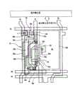
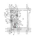
接着,针对具备这种像素电路的像素布局(layout),参照图5与第6A图、第6B图进行说明。图5所示为1个像素的概略平面构造图,图6A与图6B分别显示沿图5的A-A线、B-B线的概略剖面构造。Next, a pixel layout (layout) including such a pixel circuit will be described with reference to FIG. 5 , FIG. 6A , and FIG. 6B . FIG. 5 is a schematic plan view of a pixel, and FIG. 6A and FIG. 6B respectively show a schematic cross-sectional structure along the lines A-A and B-B of FIG. 5 .
在玻璃等透明绝缘基板100上形成缓冲层102,形成在其上方且由多晶硅所构成的各TFT主动层以及构成电容电极的半导体层(120、124、28e),在图5中由虚线所示。此外,在图5中,形成于较上述半导体层更上方,采用Cr等高融点金属材料的栅极线GL、电容线SC、及修正TFT 22的栅极22g、及驱动TFT 24的栅极24g由虚实相见的线表示。另外,形成于较半导体层、上述GL、SC更上方,采用Al等低电阻金属材料的数据线DL、电源线PL、与这些为同层的金属配线24w以实线表示。A
在图5所示的布局中,各像素的构成位于沿显示装置的水平扫描(H)方向所形成的栅极线GL的行间的位置处,以及大概沿显示装置的垂直扫描(V)方向所形成的数据线DL的行间的位置处。此外,电源线PL形成于与数据线DL大致并排并朝垂直扫描方向(矩阵的列方向),在各像素区域内,通过数据线DL、与连接于此数据线DL的像素的有机EL组件26之间。然后,如后述,选择TFT 20、修正TFT 22及保持电容28配置于数据线DL与电源线PL之间,驱动TFT与有机EL组件26配置于电源线PL与相邻列的数据线DL之间。In the layout shown in FIG. 5, the configuration of each pixel is located at a position between rows of gate lines GL formed along the horizontal scanning (H) direction of the display device, and approximately along the vertical scanning (V) direction of the display device. The position between the rows of the formed data line DL. In addition, the power line PL is formed approximately in parallel with the data line DL and faces the vertical scanning direction (column direction of the matrix), and in each pixel area, passes through the data line DL and the
选择TFT 20形成于栅极线GL与数据线DL的交叉点附近。从栅极线GL朝像素区域形成突出部,在层间夹介着栅极绝缘膜104,并以横跨沿栅极线GL延伸的半导体层120的一部分的方式予以覆盖。从此栅极线GL突出的突出部便成为TFT 20的栅极电极20g,半导体层120的被此栅极电极20g覆盖的区域将成为沟道区域。The
连接于选择TFT 20的修正TFT 22在由数据线DL与电源线PL所包夹的区域中,配置成在其沟道长度方向沿数据线DL的延伸方向(垂直扫描方向)的状态。此外,该修正TFT 22的主动层以部分重叠于数据线DL的方式,形成于数据线DL的下层。在该修正TFT 22、与靠近下一行栅极线GL所配置的电容线SC之间,更具体而言,沿该电容线SC配置保持电容28。此外,驱动TFT 24夹介着电源线PL而配置于与修正TFT 22形成区域为相反侧区域(有机EL组件区域26侧),构成其主动层的半导体层124的至少沟道区域24c配置成尽可能接近修正TFT22的沟道区域22c状态而加以布局。The
在此,于本实施形态中,选择TFT 20的主动层、修正TFT 22的主动层、及保持电容28的电容电极28e利用单一半导体层120而一体化形成(当然,也可各为独立层,且分别依预定配线进行电性连接)。Here, in this embodiment, the active layer of the
在选择TFT 20的形成区域中,数据线DL与半导体层120在贯穿栅极绝缘膜104与层间绝缘膜106而形成的接触孔(contact hole)中连接。然后,该半导体层120从数据线DL的下层区域(与数据线DL的接触区域),沿栅极线GL延伸至与电源线PL重叠的位置处,并从重叠位置将电源线PL的下层沿电源线PL的延伸方向,朝垂直扫描方向延伸。此外,此半导体层120在修正TFT 22的栅极22g与电源线PL的接触附近前方,从电源线PL的下层位置起,朝平行于栅极线GL延伸方向的方向弯曲,并朝数据线DL延伸。In the formation region of the
另外,在选择TFT 20的形成区域中,半导体层120,连接于数据线DL的杂质植入区域构成第1导电区域(例如:漏极区域20d),重叠于栅极20g的无杂质植入的本征区域(intrinsic range)将构成沟道区域20c,在夹介着此沟道区域20c的相反侧,构成经植入与第1导电区域相同导电型之杂质的第2导电区域(例如源极区域20s)。In addition, in the formation region of the
从电源线PL的下层朝数据线DL延伸的半导体层120,在与数据线DL再度交叉的附近(选择TFT 20的第1导电区域20d附近),将朝数据线DL延伸方向弯曲,且至少一部分重叠于电源线PL形成区域(在此例中,与数据线DL均部分重叠),并将数据线DL与电源线PL间的区域,朝垂直扫描方向延伸至电容线SC形成区域为止。The
再者,半导体层120沿数据线DL配置的区域构成修正TFT 22的主动层,在夹介着该主动层的栅极绝缘膜104的上方配置有修正TFT22的栅极电极22g,该栅极电极22g透过形成于层间绝缘膜106的接触孔而连接于电源线PL。该栅极电极22g从与电源线PL的接触位置朝数据线DL延伸,并在与半导体层120(修正TFT22的主动层)重叠的位置处弯曲,朝数据线DL的延伸方向延伸,并覆盖半导体层120的上层,且依部分重叠数据线DL与电源线PL的方式,形成于该等的下层。Furthermore, the region of the
半导体层120的被栅极电极22g覆盖的区域形成修正TFT 22的未施行杂质掺杂的沟道区域22c,夹介着沟道区域22c而在选择TFT20侧形成经植入与该选择TFT 20不同导电型的杂质的第1导电区域(在此,例如源极区域22s),在电容线SC侧形成经植入与第1导电区域22s为相同杂质的第2导电区域(在此为漏极区域22d)。另外,数据线DL、电源线PL、及此修正TFT 22的至少沟道区域22c,将与这些线部分重叠,并形成于该等的下层,借此可有效率的将修正TFT 22配置于数据线DL与电源线PL之间非常狭窄的区域内。此外,通过将栅极电极22g配置于该沟道区域22c及数据线DL与电源线PL的层间,沟道区域22c便将电性屏蔽于数据线DL,可防止修正TFT 22的动作受到施加于数据线DL的数据信号的影响。此外,因为至少修正TFT 22的栅极电极22g连接于电源线PL,因此即便该修正TFT 22的主动层,特别沟道区域22c配置成重叠于电源线PL的状态,对沟道区域22c所施加的电压与覆盖栅极电极22g的情况无实质变化。所以,便可将修正TFT 22的主动层的大半区域形成于电源线PL的下层,依照这种配置的话,在1个像素内的开口率,即有助于发光的有机EL组件26的形成面积便可形成最大极限。The region of the
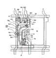
半导体层120从修正TFT 22的第2导电区域形成区域朝电容线SC延伸,在与电容线SC交叉的位置处弯曲,在朝电容线SC的延伸方向即水平扫描方向,依此电容线SC与其间夹介着栅极绝缘膜104并重叠的方式施行图案化处理(patterning),半导体层120的重叠于电容线SC的区域便具有电容电极(第1电极)28e的功能,电容线SC(第2电极)与该电容电极28e,在其间夹介栅极绝缘膜104而相对向配置的区域便形成保持电容28。The
在修正TFT 22的第2导电区域22d与保持电容28的电容电极28e间,透过形成于层间绝缘膜106与栅极绝缘膜104的接触孔,连接金属配线24w。该金属配线24w沿电容线SC的延伸方向形成,在形成于层间绝缘膜106的接触孔中,与驱动TFT 24的栅极电极24g相连接。Between the second
驱动TFT 24的栅极电极24g从其和金属配线24w的连接区域沿自行的栅极线GL的形成方向(图中为朝上方向)延伸,并在中途横跨电源线PL的下层,于电源线PL的有机EL组件26侧沿该电源线PL的延伸方向形成。The
在此,电源线PL将从与修正TFT 22的栅极电极22g的接触区域附近起,弯曲接近数据线DL,在上述金属配线24w附近,朝有机EL组件26侧弯曲迂回该形成区域,并从与构成驱动TFT 24的主动层的半导体层124相接触附近起,朝下一行像素延伸于垂直扫描方向。然后,驱动TFT 24通过电源线PL靠近数据线DL侧,而形成有机EL组件26间的隔间(space)。Here, the power line PL bends from the vicinity of the contact area with the
构成驱动TFT 24的主动层的半导体层124,在上方被栅极电极24g所覆盖的区域形成有沟道区域24c,与电源线PL的连接侧形成有第1导电区域(在此为源极区域24s),更在与有机EL组件26的连接侧形成第2导电区域(在此为漏极区域24d)。沟道区域24c未掺杂杂质的本征区域,形成于其两侧的第1与第2导电区域(24s与24d),则掺杂与上述修正TFT 22为相同导电型的杂质。另外,驱动TFT 24的第1导电区域24s在形成于层间绝缘膜106与栅极绝缘膜104的接触孔中,与电源线PL相连接。此外,驱动TFT 24的第2导电区域24d在形成于层间绝缘膜106与栅极绝缘膜104的接触孔中,与例如由与上述电源线PL等为相同材料所构成的连接电极24e相连接。In the
再者,如图6A及图6B所示,在覆盖数据线DL、电源线PL、上述金属配线24w、连接电极24e的基板整面上,形成有用以使上面平而化的由有机树脂等构成的平面化绝缘层108。然后,在该平面化绝缘层108中,于连接于上述驱动TFT 24的连接电极24e形成区域中形成接触孔,并透过该接触孔,将形成于该平面化绝缘层108上的有机EL组件26的第1电极262(在此为阳极)与连接电极24e相连接。另外,当未设置连接电极24e的情况时,在驱动TFT 24的第2导电区域24d形成区域中,形成贯穿平面化绝缘层108、层间绝缘膜106、与栅极绝缘膜104的接触孔,直接将有机EL组件26的第1电极262与第2导电区域24d连接。Furthermore, as shown in FIG. 6A and FIG. 6B, on the entire surface of the substrate covering the data line DL, the power line PL, the above-mentioned
如图6B所示,有机EL组件26形成于基板侧,且对于连接于驱动TFT 24的每个像素,在各自图案的第1电极262与第2电极264之间,设有发光组件层270。第1电极262可采用如ITO(Indium Tin Oxide)等透明导电性金属氧化物等所形成,在此具有阳极(空穴植入电极)的功能。第2电极264由如Al、Ag等功函数(仕事関数)较小的金属材料,或这种金属材料与上述ITO等的积层构造所构成,在此具有阴极(电子植入电极)的功能。另外,将每个像素形成各自图案的第1电极262的边缘部分,利用形成在平面化绝缘层108更上层的第2平面化绝缘层110而覆盖,以防止在形成非常薄的发光组件层270上所形成的第2电极264与此第1电极262间发生短路现象。As shown in FIG. 6B, the
发光组件层270在这个例子中为空穴输送层272、发光层274、电子输送层276等3层构造。不仅限于3层构造,随所使用的有机材料等,可为具备发光功能的单层,可为双层,可为4层以上的积层构造。当发光组件层270采多层构造的情况时,可全层形成各像素共通的情况,也可以多层中的一部分或全层,例如图6B所示,仅发光层274形成如同第1电极262,依每个像素设定个别图案。In this example, the light-emitting
这种构造的有机EL组件26,在本实施例中从电源线PL经由驱动TFT 24供应给第1电极262的电流在与第2电极264之间流通,并以对应电流量的辉度,在发光组件层中引起发光。另外,发光是通过从第1电极262所植入的空穴、与从第2电极264所植入的电子,在发光组件层中再结合,借此被激发的发光分子在返回基层状态之际便进行发光而得的,在本例中,辨识到光穿透过透明的第1电极262与基板100,并从基板射出于外部。In the
在本实施例中,如上述,夹介着电源线PL且上述修正TFT 22与驱动TFT 24配置成尽可能靠近的布局。特别修正TFT 22的沟道区域22c与驱动TFT 24的沟道区域24c,其沟道区域的至少一部分在垂直扫描方向上形成相互并排的状态。In this embodiment, as described above, the
在本实施例中,形成于像素内的各TFT的主动层,对于利用电浆CVD等所形成的非晶硅层,将整形为线状(line)的脉冲激光(参照图5)设定成其长度方向在水平扫描方向为一致的状态,在其宽度方向相隔预定间距偏移并依序施行照射,而使用经多结晶化退火所获得的低温多晶硅(LTPS)层。激光束的扫描方向此激光束的宽度方向,且使其与数据线DL等的延伸方向即垂直扫描方向相一致。如图5所示,修正TFT 22与驱动TFT 24的各沟道区域22c、24c配置成其沟道长度方向一致于数据线DL等的延伸方向,即一致于激光束的扫描方向的状态。所以,通过将激光束的扫描间距设为小于修正TFT 22与驱动TFT 24的沟道长度,便可对任一沟道区域22c、24c,在其沟道长度方向中,依横跨沟道的方式(沟道宽度方向),必定照射若干次激光束。借此,即便在各激光束的能量产生偏差的情况下,因为对任一沟道区域22c、24c照射若干次激光束,因此便可在任何像素中,将所有沟道长度方向中所接收到的能量总量的偏差缩小。In this embodiment, the active layer of each TFT formed in the pixel is set to a pulsed laser beam shaped into a line (see FIG. 5 ) for an amorphous silicon layer formed by plasma CVD or the like. Its length direction is in the same state in the horizontal scanning direction, and its width direction is shifted at predetermined intervals and sequentially irradiated, and a low-temperature polysilicon (LTPS) layer obtained by polycrystallization annealing is used. The scanning direction of the laser beam is the width direction of the laser beam, and is made to coincide with the extending direction of the data lines DL, ie, the vertical scanning direction. As shown in FIG. 5 , the
再者,当将利用所谓激光退火而形成的多晶硅层使用在TFT的主动层的情况时,便依将同一脉冲激光束同时照射在构成修正TFT 22与驱动TFT 24的沟道区域22c、24c的区域的方式,将沟道区域22c、24c相靠近配置,借此可轻易地在两个TFT上,同等的形成对TFT特性(特别临限值)具有颇大影响的多结晶化状态。Furthermore, when the polysilicon layer formed by so-called laser annealing is used as the active layer of the TFT, the same pulsed laser beam is simultaneously irradiated on the
其中,经整形为线状的脉冲激光的1个照射区域,例如脉冲长度方向为10cm至30cm的长度,其脉冲宽度为300μm左右。然后,这种大小的脉冲激光的扫描间距例如以25μm左右,即,一边以每隔25μm偏移脉冲激光的照射位置,一边将非晶硅进行多结晶化。此外,将修正TFT 22的沟道区域22c、与驱动TFT 24的沟道区域24c,不仅相靠近的配置,且通过在朝交叉于垂直扫描方向的方向可拉出的同一直线,至少一部分配置成并排的状态,借此可将同一脉冲激光照射于各沟道区域22c、24c。此外,将修正TFT 22与驱动TFT 24的双方,都设定为其沟道长度至少在30μm以上,优选的是40μm以上,借此可将如上述大小的脉冲激光依如上所述的间距,沿像素的垂直扫描方向对沟道形成区域进行扫描,借此便可确实的将至少1个以上的同一脉冲激光照射于2个TFT的沟道区域22c、24c。Among them, one irradiated region of the pulsed laser light shaped into a line has a length of, for example, 10 cm to 30 cm in the pulse length direction, and its pulse width is about 300 μm. Then, the scanning pitch of the pulsed laser light of such a size is, for example, about 25 μm, that is, the amorphous silicon is polycrystallized while shifting the irradiation position of the pulsed laser light every 25 μm. In addition, the
再者,同一导电型的杂质以各栅极22g、24g为屏蔽(mask),而同时植入于半导体层120与124,因为形成位置非常接近,因此便可整合杂质植入条件(植入浓度、植入能量等),由此观点来看也可修正TFT 22与驱动TFT 24的特性使其相等。Furthermore, the impurities of the same conductivity type are implanted into the semiconductor layers 120 and 124 at the same time using the
通过将像素区域内形成如上述所说明的布局,在像素区域的水平扫描方向的单侧区域(图5的像素左侧)配置数据线DL、电源线、及TFT20、22、24等电路组件,在剩下的单侧(图5的像素右侧)配置有机EL组件26,整体便可形成有效率的配置。具体而言,通过这种布局,便可在各像素区域内将有机EL组件26尽量形成较大,且有助于提升作为显示装置的开口率。此外,当考虑发光效率及需求亮度时,依每个发光颜色切换像素面积,而整合各像素的寿命的情况时,也可不须变更TFT 20、22、24、保持电容28等的面积或布局,即可仅轻易变更有机EL组件26的面积,而可达到提升设计效率的效果。By forming the layout as described above in the pixel area, the data line DL, power line, and TFT20, 22, 24 and other circuit components are arranged in the single-side area (the left side of the pixel in FIG. 5 ) in the horizontal scanning direction of the pixel area, The
再者,如图5所示的布局,矩阵配置的像素采取每行的同色像素位置仅朝水平扫描方向偏移预定间距的所谓三角形(デルタ)排列,当一条数据线DL为将数据信号Vdata供应给同色像素的情况时,如图5所示,数据线DL朝矩阵的列方向蛇行延伸,并连接于在线的左右交错配置的同色像素的选择TFT 20。通过采用这种布局,在图5所示的像素的下一行像素中,上述有机EL组件26与图5相反的配置于像素左侧,TFT 20、22、24等则配置于像素右侧。当然,在上述说明的布局中,不仅限于三角形排列,也可为直线排列,在这种情况下,每行的有机EL组件、与用以控制该有机EL组件的TFT等的位置关并没有左右反转。Furthermore, in the layout shown in FIG. 5 , the pixels of the matrix configuration adopt a so-called delta arrangement in which the positions of pixels of the same color in each row are only offset by a predetermined distance in the horizontal scanning direction. When a data line DL is used to supply the data signal Vdata In the case of pixels of the same color, as shown in FIG. 5 , the data line DL snakes along the column direction of the matrix, and is connected to the
在此,本实施例所涉及的修正TFT 22如图5所示,由半导体层所构成的沟道区域22c的宽度(沟道宽度)在其沟道长度方向发生变化。具体而言,在图5中,越靠近选择TFT 20(图中上侧)宽度越宽,在保持电容28与驱动TFT 24的连接侧(图中下侧)宽度将变狭窄。依此修正TFT 22的沟道宽度在其沟道长度方向,设置至少不同于其它的部分,便可增加修正TFT 22的配置自由度。另外,修正TFT 22的特性可考虑以最狭窄的沟道宽度为基准。依此,通过提高修正TFT 22的配置自由度,便可有效的执行其它电路组件的驱动TFT 24的栅极24g的布局等。此外,为求能增加配置的自由度,优选的是,变更形成沟道区域的半导体层的宽度(沟道宽度方向),也可变更其它选择TFT 20、驱动TFT 24等的沟道宽度,更加提高配置的自由度。Here, in the
再者,如上所述,实施形例所涉及的像素电路配置成矩阵状,而构成显示装置。多数情况在玻璃基板上,形成包含有机EL组件的像素区域,以及在其外围用以驱动各像素的外围驱动电路,形成的顺序是,首先在基板上形成像素区域中有机EL组件以外的电路组件与外围驱动电路,然后,在这些电路组件的上方形成有机EL组件,再从组件侧使封装基板覆盖玻璃基板100并粘着,而获得有机EL面板。另外,实施例所涉及的像素电路并不仅限于这种有机EL面板,可适用于其它各种显示装置。特别当适用于在各像素中形成电流驱动型显示组件与控制此组件的电路(TFT)的情况时,仍可获得相同的效果。Furthermore, as described above, the pixel circuits according to the embodiment are arranged in a matrix to form a display device. In most cases, on a glass substrate, a pixel area including an organic EL element is formed, and a peripheral drive circuit for driving each pixel is formed on its periphery. The order of formation is first to form circuit elements other than the organic EL element in the pixel area on the substrate Then, an organic EL module is formed on these circuit components, and the package substrate is covered with the
接着,在本实施例中,优选的是,选择TFT 20、修正TFT 22多栅极化。这是因为特别将多晶硅层作为主动层使用的TFT,可有效减少较多的漏电流之故。漏电流在本实施例中,当修正TFT 22、选择TFT 20为关断时,透过这些TFT,流向数据线DL的电流,通过将这些TFT多栅极化,便可抑制漏电流。如图7所示,也可以仅将修正TFT 22施行多栅极化,或者也可仅将选择TFT 20施行多栅极化。当然,也可如图9所示,将二者施行多栅极化。Next, in this embodiment, it is preferable to select the
图7所示将修正TFT 22多栅极化时的等效电路,图8所示为实现该等效电路布局的一例的平面图。在图7的例子中,修正TFT 22采用所谓的双栅极构造。具体而言,在节点Tg24与选择TFT 20之间设置:漏极连接于节点Tg24的第1修正TFT 22-1,以及设置在此第1修正TFT 22-1与选择TFT 20之间的第2修正TFT 22-2等二组件。第1与第2修正TFT 22-1、22-2的栅极均连接于电源线PL,第1与第2修正TFT22-1、22-2的源极漏极电性串联连接于选择TFT 20与节点Tg24之间。由此形成这种连接关系,以提高驱动TFT 24与选择TFT 20之间的非导通漏电流耐性,而可有效防止保持于保持电容28的驱动TFT24的栅极电压Vg24泄漏于数据线DL而发生从适当数值偏移的变动的效果。FIG. 7 shows an equivalent circuit when the
具体说明的话,通过分割修正TFT 22,在第1与第2修正TFT 22-1与22-2的连接点,将选择TFT 20的源极侧的电压Vs20(修正TFT 22-2的源极电压Vd22-2)与节点Tg24的电压Vg24予以分压,其间的数值的电压Vm便成为第1修正TFT 22-1的源极电压。TFT的非导通漏电流当TFT的漏极源极间电压Vds降低1V时,便将降低约1位数。所以,通过将修正TFT 22分割,便可将漏极连接于节点Tg24的第1修正TFT22-1的漏极源极间电压Vds缩小,而降低非导通漏电流。Specifically, by dividing the
另外,如图7所示,当将修正TFT 22多栅极化时,其导电区域(在此为漏极)连接于驱动TFT 24的栅极的第1修正TFT 22-1,其沟道区域尺寸未必要与另一方例如第2修正TFT 22-2的沟道区域尺寸相同。In addition, as shown in FIG. 7, when the
例如,将第1修正TFT 22-1的沟道区域尺寸设为较小于第2修正TFT 22-2的沟道区域尺寸,借此可减小第1修正TFT 22-1的栅极电容Cg22-1。当修正TFT 22为关断时,若从此栅极电容Cg22流入于保持电容28的电荷量较多时,节点Tg24的电位经长时间仍可维持于较高状态,随电容线SC下降的电压下降速度将变迟缓。所以,通过缩小第1修正TFT 22的沟道尺寸,在关断时,流入保持电容28的来自第1修正TFT 22-1的栅极电容Cg22-1的电荷量将减少,而可迅速降低节点Tg24的电压。在这种情况下,若将第1修正TFT 22-1的沟道区域的沟道长度设为L1、沟道宽度设为W1、将第2修正TFT 22-2的沟道区域的沟道长度设为L2、沟道宽度设为W2时,优选的是,满足W1×L1<W2×L2。For example, setting the channel region size of the first modified TFT 22-1 to be smaller than the channel region size of the second modified TFT 22-2, thereby reducing the gate capacitance Cg22 of the first modified TFT 22-1 -1. When the
第1修正TFT 22-1的沟道长度L1,在满足降低非导通漏电流要求的最低极限程度的前提下,尽可能的缩短,沟道宽度W1则在布局限制所容许的范围内,尽可能的加宽。第2修正TFT 22-2的沟道长度L2越长,虽可使从此第2修正TFT 22-2的栅极电容Cg22-2流入节点Tg24的电荷的流出迟缓,但是如此一来,TFT的导通电阻将变大,数据写入时间将拉长。所以,优选的是,依L2/W2的值变小的方式,即L2增长份量恰为宽度W2加宽份量。由此观点来看,优选的是,满足上述W1×L1<W2×L2。The channel length L1 of the first modified TFT 22-1 is shortened as much as possible under the premise of meeting the minimum limit of the non-conduction leakage current requirement, and the channel width W1 is within the allowable range of layout restrictions, as much as possible. possible widening. The longer the channel length L2 of the second modified TFT 22-2 is, the longer the outflow of charges flowing into the node Tg24 from the gate capacitance Cg22-2 of the second modified TFT 22-2 can be slowed down. The on-resistance will become larger, and the data writing time will be longer. Therefore, preferably, according to the way that the value of L2/W2 becomes smaller, that is, the amount of increase of L2 is exactly the amount of widening of the width W2. From this point of view, it is preferable that the above W1×L1<W2×L2 is satisfied.
图8所示如上述,将修正TFT 22多栅极化时的布局的一例平面构造。在图8的例子中,选择TFT 20的主动层与修正TFT 22的主动层,利用同一半导体层而一体形成,但为方便说明,对于构成第1修正TFT22-1、22-2的主动层的半导体层标注图标符号122。该半导体层122如同上述图5的布局,沿数据线DL并朝相邻行方向(图中下方)延伸。FIG. 8 shows an example of the planar structure of the layout when the modified
修正TFT 22-1、22-2的栅极22g(22g1、22g2)共通的在电源线PL的下层区域与该电源线PL相连接。所以,该栅极电极22g便从接触于电源线PL的位置起,朝数据线DL延伸于水平扫描方向,横跨主动层122上方的区域将构成第2修正TFT 22-2的栅极电极22g2,从此处更延伸至数据线DL的形成区域,在刚横跨数据线DL之后便返折,而钻入数据线DL下方。在钻入数据线DL后的附近,栅极电极22g将依再覆盖主动层122上方的方式,沿数据线DL的延伸方向朝下一行像素方向延伸,在此重叠于主动层122的区域便成为第1修正TFT 22-1的栅极电极22g1。另外,此第1修正TFT 22-1的栅极电极22g1形成于电源线PL与主动层122的层间,主动层122便电性阻隔形成于其上方的电源线PL与数据线DL。The
依此,将栅极电极22g返折成U形图案,借此可覆盖沿数据线DL朝垂直扫描方向延伸的半导体层122上方例如2个地方,可在分别被栅极电极22g所覆盖的位置各自形成沟道区域22c2、22c1。半导体层122从连接于第2修正TFT22-2的选择TFT20的源极区域20s侧起,依序形成源极区域22s2、沟道区域22c2(栅极电极22g2的下层区域)、第2修正TFT 22-2的漏极区域22d2及第1修正TFT 22-1的源极区域22s1、沟道区域22c1(栅极电极22g1的下层)、及第1修正TFT 22-1的漏极区域22d1。然后,第1修正TFT 22-1的漏极区域22d1连接保持电容28的电容电极28e(同一半导体层),且透过金属配线24w与驱动TFT 24的栅极电极24g相连接。According to this, the
若采用图8所示布局的话,即便将修正TFT 22多栅极化(在此为[双栅极化]),仍可极力抑制其设置面积的增加。If the layout shown in FIG. 8 is adopted, even if the
图9所示的不仅修正TFT 22,就连上述选择TFT 20页施行多栅极化情况时的电路构造例。此外,图10所示是采用图9所示电路构造时的实际布局一例平面图。在图9的例子中,由串联连接于数据线DL的2个选择TFT20-1、20-2构成选择TFT。另外,2个选择TFT 20-1、20-2的栅极均连接于栅极线GL。Fig. 9 shows not only the
为将选择TFT 20施行多栅极化,对如图5等所示的选择TFT 20的单栅极构造布局,施加简单的变更便可轻易的对应。例如图10所示,构成选择TFT 20的主动层的半导体层120在选择TFT 20的形成区域附近,形成从数据线DL在电源线PL处返折为U形(ㄈ形)的形状。所以,仅要将从栅极线GL突出形成的栅极电极20g的图案,形成如图10中虚线所示,更进一步的延长并重叠于从电源线PL返折的半导体层120上层状态的话便可。依此延伸栅极电极20g,在靠近返折呈U形的半导体层120的栅极线GL附近侧,与返折侧的2个地方形成栅极电极20g1、20g2,并通过在各自下层形成沟道区域20c1、20c2,便可轻易地形成其主动层电性串联连接于数据线DL的双栅极型选择TFT20。此外,再如图10所示,从栅极电极20g中途更朝水平扫描方向设置突出部,便可由将主动层的U形底边部分的上层覆盖此突出部的方式,获得3个主动层串联连接于数据线DL的三栅极型选择TFT 20。In order to implement
图11所示修正TFT 22的多栅极(双栅极)化的另一布局例。在图11的布局中,从朝水平扫描方向延伸的栅极线GL,由与数据线DL的接触区域起,沿该栅极线GL朝水平扫描方向配置半导体层120,朝该半导体层120并排突出形成2个栅极电极20g1、20g2。在该例子中,多栅极的选择TFT 20的沟道区域20c1、20c2并排配置于栅极线GL的延伸方向即水平扫描方向。Another layout example of multi-gate (double gate)
如上述图9及图10、或图11所示,不仅修正TFT 22,甚至将选择TFT 20多栅极化,借此可更有效的抑制非导通漏电流。As shown in FIG. 9 and FIG. 10, or FIG. 11 above, not only the
图12所示为另一电路构造例。在图12所示的平均1个像素的等效电路构造中,在一端(第1导电区域:例如漏极)连接于数据线DL的选择TFT 20的另一端(第2导电区域:例如源极)与上述修正TFT 22的第1导电区域(例如源极)之间,更具备有栅极连接于电容线SC的抑制漏电流TFT 30。此抑制漏电流TFT 30是n沟道型,与修正TFT 22呈相反极性。Fig. 12 shows another circuit configuration example. In the equivalent circuit structure of an average pixel shown in FIG. ) and the first conductive region (for example, the source) of the
该抑制漏电流TFT 30电容线SC呈H电位时便导通,呈L电位时便关断。所以,栅极线GL在H电位期间导通,在关于将数据线DL的数据电压Vdata写入于驱动TFT 24的栅极方面,均不致发生问题。此外,在资料写入结束之后,因为电容线SC降低为L电位,因而关断。即,当电容线SC下降,驱动TFT 24的栅极电位转为低电压的情况时,该抑制漏电流TFT 30便维持关断状态,便可有效的抑制从此时的数据线DL朝驱动TFT 24的栅极流通的漏电流。所以,将可更加提升显示装置内的若干像素的各发光辉度的均匀状况。另外,在图12所示构造中,虽可更将修正TFT 22多栅极化,便可更加降低非导通漏电流,但是电路组件的增加将导致开口率下降。所以,在开口率取最大极限,且可达各像素发光辉度均匀的范围内,决定是否更进一步将修正TFT多栅极化较为适合。The leakage
产业上之可利用性Industrial availability
可利用在各像素具有显示组件的显示装置等。A display device or the like having a display element in each pixel can be used.
Claims (19)
Applications Claiming Priority (3)
| Application Number | Priority Date | Filing Date | Title |
|---|---|---|---|
| JP378581/2003 | 2003-11-07 | ||
| JP2003378581 | 2003-11-07 | ||
| JP154092/2004 | 2004-05-25 |
Publications (2)
| Publication Number | Publication Date |
|---|---|
| CN1875394A CN1875394A (en) | 2006-12-06 |
| CN100419835Ctrue CN100419835C (en) | 2008-09-17 |
Family
ID=37484945
Family Applications (1)
| Application Number | Title | Priority Date | Filing Date |
|---|---|---|---|
| CNB2004800323727AExpired - LifetimeCN100419835C (en) | 2003-11-07 | 2004-11-08 | Pixel circuit and display device |
Country Status (1)
| Country | Link |
|---|---|
| CN (1) | CN100419835C (en) |
Cited By (1)
| Publication number | Priority date | Publication date | Assignee | Title |
|---|---|---|---|---|
| CN105976762A (en)* | 2011-03-10 | 2016-09-28 | 精工爱普生株式会社 | Electro-optical device and electronic apparatus |
Families Citing this family (6)
| Publication number | Priority date | Publication date | Assignee | Title |
|---|---|---|---|---|
| JP4524699B2 (en)* | 2007-10-17 | 2010-08-18 | ソニー株式会社 | Display device |
| KR101991338B1 (en)* | 2012-09-24 | 2019-06-20 | 엘지디스플레이 주식회사 | Thin film transistor array substrate and method for manufacturing of the same |
| TWI566395B (en)* | 2013-11-18 | 2017-01-11 | 元太科技工業股份有限公司 | Organic light emitting diode display and manufacturing method thereof |
| KR102047513B1 (en)* | 2016-04-29 | 2019-11-22 | 삼성디스플레이 주식회사 | Display device |
| CN106932968B (en)* | 2017-05-11 | 2019-07-05 | 京东方科技集团股份有限公司 | A kind of display panel and display device |
| CN110728952B (en)* | 2019-10-31 | 2021-04-30 | 厦门天马微电子有限公司 | Pixel driving circuit, driving method thereof and display device |
Citations (5)
| Publication number | Priority date | Publication date | Assignee | Title |
|---|---|---|---|---|
| EP1003150A1 (en)* | 1998-03-18 | 2000-05-24 | Seiko Epson Corporation | Transistor circuit, display panel and electronic apparatus |
| JP2001042826A (en)* | 1999-07-30 | 2001-02-16 | Pioneer Electronic Corp | Active matrix type light emitting panel and display device |
| CN1405750A (en)* | 2001-09-10 | 2003-03-26 | 精工爱普生株式会社 | Unit circuit, electronic circuit, electronic device, electro-optical device, driving method, and electronic device |
| US20030132931A1 (en)* | 2001-10-30 | 2003-07-17 | Hajime Kimura | Semiconductor device and driving method thereof |
| CN1440013A (en)* | 2003-02-24 | 2003-09-03 | 统宝光电股份有限公司 | Pixel Driving Circuit in Active Array Electroluminescence Display |
- 2004
- 2004-11-08CNCNB2004800323727Apatent/CN100419835C/ennot_activeExpired - Lifetime
Patent Citations (5)
| Publication number | Priority date | Publication date | Assignee | Title |
|---|---|---|---|---|
| EP1003150A1 (en)* | 1998-03-18 | 2000-05-24 | Seiko Epson Corporation | Transistor circuit, display panel and electronic apparatus |
| JP2001042826A (en)* | 1999-07-30 | 2001-02-16 | Pioneer Electronic Corp | Active matrix type light emitting panel and display device |
| CN1405750A (en)* | 2001-09-10 | 2003-03-26 | 精工爱普生株式会社 | Unit circuit, electronic circuit, electronic device, electro-optical device, driving method, and electronic device |
| US20030132931A1 (en)* | 2001-10-30 | 2003-07-17 | Hajime Kimura | Semiconductor device and driving method thereof |
| CN1440013A (en)* | 2003-02-24 | 2003-09-03 | 统宝光电股份有限公司 | Pixel Driving Circuit in Active Array Electroluminescence Display |
Cited By (2)
| Publication number | Priority date | Publication date | Assignee | Title |
|---|---|---|---|---|
| CN105976762A (en)* | 2011-03-10 | 2016-09-28 | 精工爱普生株式会社 | Electro-optical device and electronic apparatus |
| CN105976762B (en)* | 2011-03-10 | 2019-12-06 | 精工爱普生株式会社 | Electro-optical device and electronic apparatus |
Also Published As
| Publication number | Publication date |
|---|---|
| CN1875394A (en) | 2006-12-06 |
Similar Documents
| Publication | Publication Date | Title |
|---|---|---|
| JP4180018B2 (en) | Pixel circuit and display device | |
| US7324075B2 (en) | Pixel circuit and display device | |
| KR101046415B1 (en) | Pixel circuit and display device | |
| TWI402801B (en) | Organic electroluminescent device and organic electroluminescent display device | |
| CN100533528C (en) | display device | |
| KR102047513B1 (en) | Display device | |
| KR20200064230A (en) | Organic light emitting diode display device | |
| US8730134B2 (en) | Pixel circuit and display device | |
| CN100403377C (en) | image display device | |
| JP2009258330A (en) | Display apparatus | |
| JP2003173154A (en) | Semiconductor device and display device | |
| JP2009109853A (en) | Active matrix type display device | |
| KR20190074812A (en) | Driving thin film transistor and organic light emitting display device comprising the same | |
| CN100419835C (en) | Pixel circuit and display device | |
| JP2004133455A (en) | Flat panel display | |
| JP4592330B2 (en) | Pixel circuit and display device | |
| JP4610228B2 (en) | Pixel circuit and display device | |
| JP4549102B2 (en) | Pixel circuit and display device | |
| JP4721656B2 (en) | Pixel circuit and display device | |
| KR100637304B1 (en) | Organic el display and active matrix substrate | |
| JP2005215609A (en) | Unit circuit, electro-optical device and electronic apparatus | |
| US20050212448A1 (en) | Organic EL display and active matrix substrate | |
| JP2010160200A (en) | Display device and method for controlling the same | |
| CN111969066B (en) | Thin film transistor, array substrate, display panel and display device | |
| KR20140120717A (en) | Thin film transistor and organic light emitting display device |
Legal Events
| Date | Code | Title | Description |
|---|---|---|---|
| C06 | Publication | ||
| PB01 | Publication | ||
| C10 | Entry into substantive examination | ||
| SE01 | Entry into force of request for substantive examination | ||
| C14 | Grant of patent or utility model | ||
| GR01 | Patent grant | ||
| CX01 | Expiry of patent term | ||
| CX01 | Expiry of patent term | Granted publication date:20080917 |