CN100413044C - Glue filling structure for wafer-level chip size packaging and method thereof - Google Patents
Glue filling structure for wafer-level chip size packaging and method thereofDownload PDFInfo
- Publication number
- CN100413044C CN100413044CCNB200510068973XACN200510068973ACN100413044CCN 100413044 CCN100413044 CCN 100413044CCN B200510068973X ACNB200510068973X ACN B200510068973XACN 200510068973 ACN200510068973 ACN 200510068973ACN 100413044 CCN100413044 CCN 100413044C
- Authority
- CN
- China
- Prior art keywords
- glued membrane
- filler structure
- substrate
- film
- glue
- Prior art date
- Legal status (The legal status is an assumption and is not a legal conclusion. Google has not performed a legal analysis and makes no representation as to the accuracy of the status listed.)
- Expired - Lifetime
Links
Images


Classifications
- H—ELECTRICITY
- H01—ELECTRIC ELEMENTS
- H01L—SEMICONDUCTOR DEVICES NOT COVERED BY CLASS H10
- H01L21/00—Processes or apparatus adapted for the manufacture or treatment of semiconductor or solid state devices or of parts thereof
- H01L21/67—Apparatus specially adapted for handling semiconductor or electric solid state devices during manufacture or treatment thereof; Apparatus specially adapted for handling wafers during manufacture or treatment of semiconductor or electric solid state devices or components ; Apparatus not specifically provided for elsewhere
- H01L21/683—Apparatus specially adapted for handling semiconductor or electric solid state devices during manufacture or treatment thereof; Apparatus specially adapted for handling wafers during manufacture or treatment of semiconductor or electric solid state devices or components ; Apparatus not specifically provided for elsewhere for supporting or gripping
- H01L21/6835—Apparatus specially adapted for handling semiconductor or electric solid state devices during manufacture or treatment thereof; Apparatus specially adapted for handling wafers during manufacture or treatment of semiconductor or electric solid state devices or components ; Apparatus not specifically provided for elsewhere for supporting or gripping using temporarily an auxiliary support
- H—ELECTRICITY
- H01—ELECTRIC ELEMENTS
- H01L—SEMICONDUCTOR DEVICES NOT COVERED BY CLASS H10
- H01L23/00—Details of semiconductor or other solid state devices
- H01L23/28—Encapsulations, e.g. encapsulating layers, coatings, e.g. for protection
- H—ELECTRICITY
- H01—ELECTRIC ELEMENTS
- H01L—SEMICONDUCTOR DEVICES NOT COVERED BY CLASS H10
- H01L23/00—Details of semiconductor or other solid state devices
- H01L23/52—Arrangements for conducting electric current within the device in operation from one component to another, i.e. interconnections, e.g. wires, lead frames
- H01L23/538—Arrangements for conducting electric current within the device in operation from one component to another, i.e. interconnections, e.g. wires, lead frames the interconnection structure between a plurality of semiconductor chips being formed on, or in, insulating substrates
- H01L23/5389—Arrangements for conducting electric current within the device in operation from one component to another, i.e. interconnections, e.g. wires, lead frames the interconnection structure between a plurality of semiconductor chips being formed on, or in, insulating substrates the chips being integrally enclosed by the interconnect and support structures
- H—ELECTRICITY
- H01—ELECTRIC ELEMENTS
- H01L—SEMICONDUCTOR DEVICES NOT COVERED BY CLASS H10
- H01L24/00—Arrangements for connecting or disconnecting semiconductor or solid-state bodies; Methods or apparatus related thereto
- H01L24/01—Means for bonding being attached to, or being formed on, the surface to be connected, e.g. chip-to-package, die-attach, "first-level" interconnects; Manufacturing methods related thereto
- H01L24/26—Layer connectors, e.g. plate connectors, solder or adhesive layers; Manufacturing methods related thereto
- H01L24/28—Structure, shape, material or disposition of the layer connectors prior to the connecting process
- H01L24/29—Structure, shape, material or disposition of the layer connectors prior to the connecting process of an individual layer connector
- H—ELECTRICITY
- H01—ELECTRIC ELEMENTS
- H01L—SEMICONDUCTOR DEVICES NOT COVERED BY CLASS H10
- H01L24/00—Arrangements for connecting or disconnecting semiconductor or solid-state bodies; Methods or apparatus related thereto
- H01L24/80—Methods for connecting semiconductor or other solid state bodies using means for bonding being attached to, or being formed on, the surface to be connected
- H01L24/83—Methods for connecting semiconductor or other solid state bodies using means for bonding being attached to, or being formed on, the surface to be connected using a layer connector
- H—ELECTRICITY
- H01—ELECTRIC ELEMENTS
- H01L—SEMICONDUCTOR DEVICES NOT COVERED BY CLASS H10
- H01L2224/00—Indexing scheme for arrangements for connecting or disconnecting semiconductor or solid-state bodies and methods related thereto as covered by H01L24/00
- H01L2224/01—Means for bonding being attached to, or being formed on, the surface to be connected, e.g. chip-to-package, die-attach, "first-level" interconnects; Manufacturing methods related thereto
- H01L2224/26—Layer connectors, e.g. plate connectors, solder or adhesive layers; Manufacturing methods related thereto
- H01L2224/28—Structure, shape, material or disposition of the layer connectors prior to the connecting process
- H01L2224/29—Structure, shape, material or disposition of the layer connectors prior to the connecting process of an individual layer connector
- H01L2224/29001—Core members of the layer connector
- H01L2224/29099—Material
- H01L2224/2919—Material with a principal constituent of the material being a polymer, e.g. polyester, phenolic based polymer, epoxy
- H—ELECTRICITY
- H01—ELECTRIC ELEMENTS
- H01L—SEMICONDUCTOR DEVICES NOT COVERED BY CLASS H10
- H01L2224/00—Indexing scheme for arrangements for connecting or disconnecting semiconductor or solid-state bodies and methods related thereto as covered by H01L24/00
- H01L2224/80—Methods for connecting semiconductor or other solid state bodies using means for bonding being attached to, or being formed on, the surface to be connected
- H01L2224/83—Methods for connecting semiconductor or other solid state bodies using means for bonding being attached to, or being formed on, the surface to be connected using a layer connector
- H01L2224/838—Bonding techniques
- H01L2224/8385—Bonding techniques using a polymer adhesive, e.g. an adhesive based on silicone, epoxy, polyimide, polyester
- H—ELECTRICITY
- H01—ELECTRIC ELEMENTS
- H01L—SEMICONDUCTOR DEVICES NOT COVERED BY CLASS H10
- H01L2924/00—Indexing scheme for arrangements or methods for connecting or disconnecting semiconductor or solid-state bodies as covered by H01L24/00
- H01L2924/01—Chemical elements
- H01L2924/01006—Carbon [C]
- H—ELECTRICITY
- H01—ELECTRIC ELEMENTS
- H01L—SEMICONDUCTOR DEVICES NOT COVERED BY CLASS H10
- H01L2924/00—Indexing scheme for arrangements or methods for connecting or disconnecting semiconductor or solid-state bodies as covered by H01L24/00
- H01L2924/01—Chemical elements
- H01L2924/01015—Phosphorus [P]
- H—ELECTRICITY
- H01—ELECTRIC ELEMENTS
- H01L—SEMICONDUCTOR DEVICES NOT COVERED BY CLASS H10
- H01L2924/00—Indexing scheme for arrangements or methods for connecting or disconnecting semiconductor or solid-state bodies as covered by H01L24/00
- H01L2924/01—Chemical elements
- H01L2924/01027—Cobalt [Co]
- H—ELECTRICITY
- H01—ELECTRIC ELEMENTS
- H01L—SEMICONDUCTOR DEVICES NOT COVERED BY CLASS H10
- H01L2924/00—Indexing scheme for arrangements or methods for connecting or disconnecting semiconductor or solid-state bodies as covered by H01L24/00
- H01L2924/01—Chemical elements
- H01L2924/01033—Arsenic [As]
- H—ELECTRICITY
- H01—ELECTRIC ELEMENTS
- H01L—SEMICONDUCTOR DEVICES NOT COVERED BY CLASS H10
- H01L2924/00—Indexing scheme for arrangements or methods for connecting or disconnecting semiconductor or solid-state bodies as covered by H01L24/00
- H01L2924/01—Chemical elements
- H01L2924/01094—Plutonium [Pu]
- H—ELECTRICITY
- H01—ELECTRIC ELEMENTS
- H01L—SEMICONDUCTOR DEVICES NOT COVERED BY CLASS H10
- H01L2924/00—Indexing scheme for arrangements or methods for connecting or disconnecting semiconductor or solid-state bodies as covered by H01L24/00
- H01L2924/06—Polymers
- H01L2924/0665—Epoxy resin
- H—ELECTRICITY
- H01—ELECTRIC ELEMENTS
- H01L—SEMICONDUCTOR DEVICES NOT COVERED BY CLASS H10
- H01L2924/00—Indexing scheme for arrangements or methods for connecting or disconnecting semiconductor or solid-state bodies as covered by H01L24/00
- H01L2924/06—Polymers
- H01L2924/078—Adhesive characteristics other than chemical
- H01L2924/07802—Adhesive characteristics other than chemical not being an ohmic electrical conductor
- H—ELECTRICITY
- H01—ELECTRIC ELEMENTS
- H01L—SEMICONDUCTOR DEVICES NOT COVERED BY CLASS H10
- H01L2924/00—Indexing scheme for arrangements or methods for connecting or disconnecting semiconductor or solid-state bodies as covered by H01L24/00
- H01L2924/095—Indexing scheme for arrangements or methods for connecting or disconnecting semiconductor or solid-state bodies as covered by H01L24/00 with a principal constituent of the material being a combination of two or more materials provided in the groups H01L2924/013 - H01L2924/0715
- H01L2924/097—Glass-ceramics, e.g. devitrified glass
- H01L2924/09701—Low temperature co-fired ceramic [LTCC]
- H—ELECTRICITY
- H01—ELECTRIC ELEMENTS
- H01L—SEMICONDUCTOR DEVICES NOT COVERED BY CLASS H10
- H01L2924/00—Indexing scheme for arrangements or methods for connecting or disconnecting semiconductor or solid-state bodies as covered by H01L24/00
- H01L2924/10—Details of semiconductor or other solid state devices to be connected
- H01L2924/11—Device type
- H01L2924/14—Integrated circuits
- H—ELECTRICITY
- H01—ELECTRIC ELEMENTS
- H01L—SEMICONDUCTOR DEVICES NOT COVERED BY CLASS H10
- H01L2924/00—Indexing scheme for arrangements or methods for connecting or disconnecting semiconductor or solid-state bodies as covered by H01L24/00
- H01L2924/15—Details of package parts other than the semiconductor or other solid state devices to be connected
- H01L2924/181—Encapsulation
Landscapes
- Engineering & Computer Science (AREA)
- Computer Hardware Design (AREA)
- Microelectronics & Electronic Packaging (AREA)
- Power Engineering (AREA)
- Physics & Mathematics (AREA)
- Condensed Matter Physics & Semiconductors (AREA)
- General Physics & Mathematics (AREA)
- Manufacturing & Machinery (AREA)
- Adhesives Or Adhesive Processes (AREA)
- Die Bonding (AREA)
- Container, Conveyance, Adherence, Positioning, Of Wafer (AREA)
- Encapsulation Of And Coatings For Semiconductor Or Solid State Devices (AREA)
Abstract
Translated fromChinese
Description
Translated fromChinese技术领域technical field
本发明是与一种晶圆级封装的填胶结构及其方法有关,特别是有关于一种利用正面朝下(top side face down)地填满胶使与晶粒表面平坦而不超过(overflowing)或凹陷(recessing)于上述晶粒表面的结构及其方法,用以增进填胶效果及提升可靠度测试中的使用寿命(life cycle)。The present invention is related to a glue-filling structure and method thereof for wafer-level packaging, in particular to a filling glue that uses top side face down to make the surface of the crystal grain flat without exceeding (overflowing) ) or recessing (recessing) on the structure and method of the surface of the above-mentioned crystal grains, which are used to improve the filling effect and the life cycle in the reliability test.
背景技术Background technique
一种具有球数组(Ball Grid Array,BGA)结构的半导体组件被发展以适用于高脚位数(high-pin-count)封装的半导体组件。在上述具有球数组结构的半导体组件中,一半导体芯片利用黏性材料黏着(mounted)于基板(base substrate)主表面上的一芯片刚性区域,数个凸块电极(bumpelectrodes)以一数组而置于上述基板背面上,其是在上述基板主表面的对面。A semiconductor device with a Ball Grid Array (BGA) structure has been developed to be suitable for semiconductor devices in high-pin-count packages. In the above-mentioned semiconductor component with a ball array structure, a semiconductor chip is mounted on a rigid area of the chip on the main surface of the base substrate by using an adhesive material, and several bump electrodes (bump electrodes) are arranged in an array. On the back surface of the above-mentioned substrate, which is opposite to the main surface of the above-mentioned substrate.
传统的芯片尺度封装(CSP)是利用一半导体晶圆切割成半导体芯片的方法形成,接着上述半导体芯片以一预定的位置而固定于一作为封装基底(package base)的基板上,并且以树脂将上述芯片密封,然后上述密封树脂与基板于上述半导体芯片之间的部分一起被切割。在另一传统的方法中,一半导体晶圆(尚未被切割成半导体芯片)附着于一基板上,然后上述晶圆以及基板一起被切割,上述切割与分离的半导体芯片以及封装基底是以一树脂密封。A conventional chip-scale package (CSP) is formed by cutting a semiconductor wafer into semiconductor chips, and then the above-mentioned semiconductor chips are fixed on a substrate as a package base (package base) at a predetermined position, and resin The chip is sealed, and then the sealing resin is diced together with the portion of the substrate between the semiconductor chips. In another conventional method, a semiconductor wafer (not diced into semiconductor chips) is attached to a substrate, and then the wafer and the substrate are diced together, and the diced and separated semiconductor chips and package substrate are formed with a resin seal.
然而,早期传统的制造方法中存在一问题,即是已切割与分离的半导体芯片是以一个接着一个的方式定位(positioning)与黏着(mounting)于上述基板上。之后的传统制造方法中也存在一问题,即是已切割与分离的半导体芯片以及封装基底是一个接着一个以树脂来密封。上述二种传统的方法皆需要一与半导体芯片个数同样多的工作程序(working processes),因此造成低产量(productivity)的缺点。However, there is a problem in the early traditional manufacturing method, that is, the diced and separated semiconductor chips are positioned and mounted on the substrate one by one. There is also a problem in the subsequent conventional manufacturing method, that is, the cut and separated semiconductor chips and package substrates are sealed with resin one by one. Both of the above two traditional methods require as many working processes as the number of semiconductor chips, thus resulting in the disadvantage of low productivity.
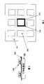
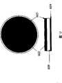
另外,目前各种型态集成电路组件封装的填胶方法是采用直接印刷填胶于晶粒之间,如图1所示。上述复数个晶粒91形成于玻璃基板90上。硅橡胶(Silicone rubber)92是利用一印刷方法形成于玻璃基板90上。一般而言,这种填胶技术会导致晶粒表面于印刷方向的过度填胶(overflow),或者在晶粒表面于非印刷方向造成凹陷(recess),其分别如图2A以及图2B所示。上述填胶可能覆盖上述晶粒的焊垫(bonding pads)。换言之,此种背景技术的填胶方法将因为晶粒表面填胶的不佳的均匀度而造成低良率以及可靠度的问题。In addition, the current glue filling method for packaging various types of integrated circuit components is to use direct printing to fill the glue between the dies, as shown in FIG. 1 . The plurality of
发明内容Contents of the invention
本发明的主要目的在于提供一种晶圆级封装的填胶结构及其方法。良好的晶粒由已制造的晶圆中选出,然后利用一挑选置放(Pick&Place)系统放置于一工具上。本发明的填胶方法可以改善晶圆级封装晶粒的良率以及可靠度。The main purpose of the present invention is to provide a glue filling structure and method for wafer level packaging. Good dies are selected from manufactured wafers and placed on a tool using a Pick&Place system. The adhesive filling method of the present invention can improve the yield rate and reliability of wafer-level packaging chips.
本发明的另一目的在于使用正面朝下填胶以使上述晶粒表面平坦化,并且使在上述晶粒表面不会产生过度(overflow)或凹陷的填胶。Another object of the present invention is to use face-down filling to planarize the surface of the die without causing overflow or depression of the filling on the surface of the die.
本发明的再一目的在于利用新的填胶方法以改善填胶效果与可靠度测试中的使用寿命(life cycle)。Another object of the present invention is to use a new glue filling method to improve the glue filling effect and the life cycle in the reliability test.
为实现上述目的,本发明提的填胶的封装结构,包括:In order to achieve the above purpose, the packaging structure of the present invention with glue filling includes:
一可移除的基板;a removable substrate;
一胶膜图案,形成于该可移除的基板上;an adhesive film pattern formed on the removable substrate;
复数个晶粒,位于该胶膜图案中;以及a plurality of dies located in the adhesive film pattern; and
一黏性材料,填满该复数个晶粒之间并且覆盖该复数个晶粒。A viscous material fills between the plurality of crystal grains and covers the plurality of crystal grains.
所述封装的填胶结构,其中该胶膜图案利用一印刷方法形成于上述可移除的基板上,其中该胶膜的材料为密封胶(seeling glue)、水溶性UV胶、可重复使用的UV胶或高熔点蜡。The glue filling structure of the package, wherein the glue film pattern is formed on the above-mentioned removable substrate by a printing method, wherein the material of the glue film is sealing glue (seeling glue), water-soluble UV glue, reusable UV glue or high melting point wax.
所述封装的填胶结构,其中该可移除的基底材料为聚硅氧、玻璃、石英或陶瓷,其中该黏性材料为一弹性材料,其中该弹性材料为硅树脂、弹性PU、多孔PU、丙烯酸橡胶、蓝膜或UV膜。The encapsulating glue filling structure, wherein the removable base material is polysiloxane, glass, quartz or ceramics, wherein the viscous material is an elastic material, wherein the elastic material is silicone resin, elastic PU, porous PU , acrylic rubber, blue film or UV film.
所述封装的填胶结构,其中该复数个晶粒是背面朝上地黏着于该胶膜图案上,该复数个晶粒的背面黏着于该黏性材料。In the encapsulating glue-filling structure, the plurality of crystal grains are adhered to the adhesive film pattern with the back facing up, and the back surfaces of the plurality of crystal grains are adhered to the adhesive material.
所述封装的填胶结构,还包括一刚性基板置于该黏性材料上,其中该刚性基板的材料包括聚硅氧、玻璃、石英、陶瓷、合金42或印刷电路板。The encapsulation filling structure further includes a rigid substrate placed on the adhesive material, wherein the material of the rigid substrate includes polysiloxane, glass, quartz, ceramic, Alloy 42 or printed circuit board.
所述封装的填胶结构,还包括一保护膜形成于该刚性基板上,其中该保护膜的材料为树脂、复合物、环氧物、聚硅氧、蓝膜、UV膜、硅橡胶、硅树脂、弹性PU、多孔PU或丙烯酸橡胶。The glue filling structure of the package also includes a protective film formed on the rigid substrate, wherein the material of the protective film is resin, composite, epoxy, polysiloxane, blue film, UV film, silicone rubber, silicon Resin, elastic PU, porous PU or acrylic rubber.
本发明提供的封装的填胶结构,还可以包括:The glue filling structure of the package provided by the present invention may also include:
复数个晶粒;以及a plurality of dies; and
一黏性材料,填满于该复数个晶粒之间并且覆盖该复数个晶粒。A viscous material is filled between the plurality of crystal grains and covers the plurality of crystal grains.
所述封装的填胶结构,其中该黏性材料为一弹性材料,其中该弹性材料为硅树脂、弹性PU、多孔PU、丙烯酸橡胶、蓝膜或UV膜。In the packaged glue filling structure, the viscous material is an elastic material, wherein the elastic material is silicone resin, elastic PU, porous PU, acrylic rubber, blue film or UV film.
所述封装的填胶结构,还包括一刚性基板置于该黏性材料的上,其中该刚性基板的材料包括聚硅氧、玻璃、石英、陶瓷、合金42或印刷电路板。The encapsulation filling structure further includes a rigid substrate disposed on the adhesive material, wherein the rigid substrate material includes polysiloxane, glass, quartz, ceramic, Alloy 42 or printed circuit board.
所述封装的填胶结构,还包括一保护膜形成于该刚性基板的上,其中该保护膜的材料为树脂、复合物、环氧物、聚硅氧、硅橡胶、硅树脂、弹性PU、多孔PU、丙烯酸橡胶、蓝膜、或UV膜,其中该保护膜系利用印刷、涂布、黏贴或铸膜方式所形成。The encapsulating glue filling structure further includes a protective film formed on the rigid substrate, wherein the material of the protective film is resin, composite, epoxy, polysiloxane, silicone rubber, silicone resin, elastic PU, Porous PU, acrylic rubber, blue film, or UV film, wherein the protective film is formed by printing, coating, pasting or casting.
附图说明Description of drawings
图1为根据公知技术的印刷填胶于形成于一玻璃基板上的晶粒之间的示意图。FIG. 1 is a schematic diagram of printing paste between dies formed on a glass substrate according to the prior art.
图2A与图2B为根据公知技术在印刷方向以及非印刷方向的填胶的示意图。2A and 2B are schematic diagrams of glue filling in the printing direction and the non-printing direction according to the known technology.
图3为本发明的黏贴一复数个晶粒于一形成于可移除基板的上的胶膜图案上的示意图。FIG. 3 is a schematic diagram of adhering a plurality of dies on an adhesive film pattern formed on a removable substrate according to the present invention.
图4为本发明的黏贴上述复数个晶粒于形成于上述可移除基板的上的胶膜图案的上的上视图。FIG. 4 is a top view of pasting the plurality of dies on the adhesive film pattern formed on the removable substrate of the present invention.
图5为本发明的填满一黏性材料于上述复数个晶粒之间并且覆盖上述复数个晶粒的示意图。5 is a schematic diagram of filling a viscous material between the plurality of crystal grains and covering the plurality of crystal grains according to the present invention.
图6为本发明的黏贴一刚性基板至上述黏性材料的示意图。FIG. 6 is a schematic diagram of adhering a rigid substrate to the adhesive material of the present invention.
图7为本发明的形成一保护膜于上述刚性基板上的示意图。FIG. 7 is a schematic diagram of forming a protective film on the above-mentioned rigid substrate according to the present invention.
图8为本发明的从上述胶膜图案中移除上述复数个晶粒的示意图。FIG. 8 is a schematic diagram of removing the above-mentioned plurality of crystal grains from the above-mentioned adhesive film pattern according to the present invention.
图9为本发明的形成一保护膜于上述刚性基板上的示意图。FIG. 9 is a schematic diagram of forming a protective film on the above-mentioned rigid substrate according to the present invention.
图10A与图10B为一晶圆与一具有铸膜复合物的晶圆的示意图。10A and 10B are schematic diagrams of a wafer and a wafer with cast film composite.
图11A与图11B为附着于基板上的晶粒铸膜前与后的示意图。11A and 11B are schematic diagrams before and after the die casting film is attached to the substrate.
图12为形成一保护膜于上述基板背面的上的示意图。FIG. 12 is a schematic diagram of forming a protective film on the back surface of the above-mentioned substrate.
具体实施方法Specific implementation method
本发明的一些实施例将详细地叙述。然而,应该了解的是除了这些明确的叙述外,本发明可以实施在一广泛范围的其它实施例中,并且本发明的范围没有明确限制于上述实施例中,其当视专利申请范围而定。此外,不同组件的部件并未依照比例显示。上述相关部件的尺寸系被扩大,并且无意义的部份将不显示,以提供本发明更清楚的叙述与理解。Some embodiments of the invention will be described in detail. However, it should be understood that the present invention may be practiced in a wide range of other embodiments than those expressly described, and that the scope of the present invention is not expressly limited to the above-described embodiments, which should be determined by the scope of the patent application. Furthermore, parts of the various assemblies are not shown to scale. The dimensions of the above-mentioned related components are exaggerated, and meaningless parts will not be shown in order to provide a clearer description and understanding of the present invention.
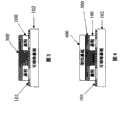
参考图3,描述本发明的黏贴复数个晶粒于一形成于可移除的暂时基板102的上的胶膜图案上。如图3所示,复数个晶粒100置放于一胶膜图案101上。上述复数个晶粒100通常利用一挑选置放(Pick&Place)系统置放于上述胶膜图案101上。上述挑选置放系统可被视为一可移动的移动芯片黏着机(Flip Chip Bonder)。上述胶膜图案101形成于一可移除的暂时基板102上。在一实施例中,上述可移除的基板102为硅橡胶、玻璃、石英或陶瓷。Referring to FIG. 3 , the present invention is described for adhering a plurality of dies on an adhesive film pattern formed on a removable
参考图4,胶膜图案101利用一印刷方法被形成于上述可移除基板102上(如图3所示)。上述参考标号(reference)200为非胶膜印刷区域。在一实施例中,上述复数个晶粒100为背部朝上地黏贴于上述胶膜图案101上。此外,每一上述复数个晶粒100的一边(称为正面)201为向下地(具有焊垫面)黏贴于上述胶膜图案101上。换言之,上述晶粒100的正面201黏贴于上述胶膜图案上。一般而言,上述正面201包含晶粒100的一切割道,因此上述晶粒100的內连线(inter-connectors)並未黏贴至上述胶膜图案101上。如图6所显示,一胶膜图案101形成于晶粒100的正面201,因此并于可移除基板102与晶粒100间形成一密闭空间。要注意的是,上述晶粒100的焊垫(bonding pads)面置于胶膜图案101上。上述复数个晶粒基本上约略对准胶膜图案的边缘以防止上述复数个晶粒的焊垫被其它材料覆盖。Referring to FIG. 4 , the
参考图5,为本发明的填满一黏性材料于上述复数个晶粒之间并且覆盖上述复数个晶粒的步骤的示意图。如图5所示,上述黏性材料300填满于复数个晶粒100之间并且覆盖上述复数个晶粒100。在一实施例中,上述黏性材料300为一弹性材料,例如硅橡胶、硅树脂、弹性PU、多孔PU、丙烯酸橡胶、蓝胶或UV胶。上述黏性材料300可以利用旋转涂布、印刷或铸膜灌胶(injection molding)形成。因此,上述复数个晶粒100为背部朝上地黏贴于上述黏性材料300上。Referring to FIG. 5 , it is a schematic diagram of the steps of filling a viscous material between the plurality of crystal grains and covering the plurality of crystal grains according to the present invention. As shown in FIG. 5 , the
此时,本发明的封装填胶结构包括一可移除基板或一临时基板102。一胶膜图案101形成在上述可移除基板102上。复数个晶粒100置放于上述胶膜图案101上。一黏性材料300填满于上述复数个晶粒100之间并且覆盖上述复数个晶粒100,如图5所示。At this time, the package filling structure of the present invention includes a removable substrate or a
参考图6,为本发明的黏贴一相对刚性基板400至上述黏性材料300的步骤的示意图,此称的相对刚性是相对于上述黏性材料300为一弹性材料而言。如图6所示,一相对刚性或称刚性基板400黏贴黏性材料300。在一实施例中,上述刚性基板400的材料包括硅橡胶、玻璃、石英、陶瓷、合金42(商用名称)或印刷电路板。在附着上述刚性基板400至上述黏性材料300之后,一UV烘烤或热烘烤的步骤可加强黏着效果。Referring to FIG. 6 , it is a schematic diagram of the steps of adhering a relatively
上述封装填胶结构还包括一刚性材料400置放于上述黏性材料300上,如图6所示。上述封装填胶结构还包括一保护膜500,形成于上述相对刚性基板400上,如图7所示。上述临时基板102可移除。The package filling structure further includes a
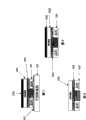
此外,一保护膜500形成于上述相对刚性基板400上,如图7所示。上述保护膜500可利用一印刷、涂布、黏贴或铸膜方法形成。在一实施例中,上述保护膜500为树脂、复合物、环氧物、硅橡胶(silicone)、硅橡胶(silicone rubber)、硅树脂、弹性PU、多孔PU、丙烯酸橡胶、蓝胶或UV胶。参考图8,为利用一特殊或特定的处理将上述胶膜图案101或上述临时基板102从上述复数个晶粒剥离(stripping)的示意图。换言之,上述胶膜图案101的表面在一般状况下具有黏性,当上述胶膜图案101置于一特殊或特定的环境中会失去黏性。上述特殊或特定的环境可能为去离子水、溶剂、根据溶液而定约略为摄氏20-40度的特定温度或特殊光(如UV光)等。通过上述特殊或特定环境的处理,上述胶膜图案101与上述晶粒100的键结(engagement)将消失。接着,上述胶膜图案101可以从上述晶粒中剥离。在一实施例中,上述胶膜图案101的材料为密封胶(seeling glue)、水溶性UV胶、可重复使用(reworkable)UV胶或高熔点蜡。In addition, a
本发明的晶圆级封装的填胶方法还包括一形成一保护膜500于上述刚性基板400背面的步骤,其作为一缓冲物(buffer),如图9所示。上述保护膜500可利用一印刷、涂布、黏贴或铸膜方式形成。在一实施例中,上述保护膜500为树脂、复合物、环氧物、硅橡胶(silicone)、硅橡胶(siliconerubber)、硅树脂、弹性PU、多孔PU、丙烯酸橡胶、蓝胶或UV胶。The glue filling method for WLP of the present invention further includes a step of forming a
本发明的一封装填胶结构包括复数个晶粒100、一黏性材料300填充于上述复数个晶粒100之间并且覆盖上述复数个晶粒。一刚性基板400置于上述黏性材料300的上,如图8所示。再者,上述封装填胶结构还包括一保护膜500形成于上述刚性基板400的上,如图9所示。A package filling structure of the present invention includes a plurality of dies 100, and an
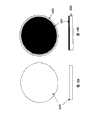
参考图10A与图10B,其为一晶圆600与一含有铸膜复合物(moldingcompound)601的晶圆600的示意图。Referring to FIG. 10A and FIG. 10B , which are schematic diagrams of a
参考图11A与图11B,其为附着于基板上的晶粒铸膜前与后的示意图。一已完成制造的晶圆切割成为复数个晶粒602,并且上述晶粒602被固定于一基板600上。一黏性材料603利用一铸膜方法灌胶填满于上述复数个晶粒602之间。Referring to FIG. 11A and FIG. 11B , which are schematic diagrams before and after the die casting film is attached to the substrate. A manufactured wafer is diced into a plurality of dies 602 , and the dies 602 are fixed on a
参考图12,其为形成一保护膜于上述基板背面的上的示意图。上述保护膜604可以利用一印刷、涂布、黏贴或铸膜方法来形成。在一实施例中,上述保护膜604为树脂、复合物、环氧物、硅橡胶(silicone)、硅橡胶(siliconerubber)、硅树脂,弹性PU、多孔PU、丙烯酸橡胶、蓝胶或UV胶。上述保护膜604可以加强上述晶圆级封装的硬度、可以利用激光或墨水作标记并且易于切割。Referring to FIG. 12 , it is a schematic diagram of forming a protective film on the back surface of the above-mentioned substrate. The
在本发明中,由铸膜/印刷方法以填胶于上述复数个晶粒100之间,其平坦度可达到+/-20微米(micron)。其与传统的直接铸膜填胶于上述晶粒之间的方法不同。因此,本发明的封装填胶方法可以避免上述晶粒表面填胶过度或凹陷,结果增进了填胶效果以及可靠度测试中的使用寿命(lifecycle)。In the present invention, glue is filled between the plurality of
虽然特殊实施例已被描述与叙述,凡熟悉此领域的技术人员,在不脱离本专利精神或范围内,所作的更动或润饰,均属于本发明所描述精神下所完成的等效改变或设计,且应包含在申请专利范围内。Although specific embodiments have been described and described, all changes or modifications made by those skilled in the art without departing from the spirit or scope of this patent belong to the equivalent changes or modifications made under the spirit of the present invention. Design, and should be included in the scope of the patent application.
Claims (10)
Applications Claiming Priority (2)
| Application Number | Priority Date | Filing Date | Title |
|---|---|---|---|
| US11/026,488US7400037B2 (en) | 2004-12-30 | 2004-12-30 | Packaging structure with coplanar filling paste and dice and with patterned glue for WL-CSP |
| US11/026,488 | 2004-12-30 |
Publications (2)
| Publication Number | Publication Date |
|---|---|
| CN1797728A CN1797728A (en) | 2006-07-05 |
| CN100413044Ctrue CN100413044C (en) | 2008-08-20 |
Family
ID=36639496
Family Applications (1)
| Application Number | Title | Priority Date | Filing Date |
|---|---|---|---|
| CNB200510068973XAExpired - LifetimeCN100413044C (en) | 2004-12-30 | 2005-04-27 | Glue filling structure for wafer-level chip size packaging and method thereof |
Country Status (7)
| Country | Link |
|---|---|
| US (2) | US7400037B2 (en) |
| JP (1) | JP2006190975A (en) |
| KR (1) | KR100693664B1 (en) |
| CN (1) | CN100413044C (en) |
| DE (1) | DE102005019553B4 (en) |
| SG (1) | SG123653A1 (en) |
| TW (1) | TWI302731B (en) |
Families Citing this family (17)
| Publication number | Priority date | Publication date | Assignee | Title |
|---|---|---|---|---|
| US8999736B2 (en)* | 2003-07-04 | 2015-04-07 | Epistar Corporation | Optoelectronic system |
| TW200807526A (en)* | 2006-07-27 | 2008-02-01 | Touch Micro System Tech | Method of wafer segmenting |
| US7830004B2 (en)* | 2006-10-27 | 2010-11-09 | Taiwan Semiconductor Manufacturing Company, Ltd. | Packaging with base layers comprising alloy 42 |
| KR100826393B1 (en) | 2007-05-22 | 2008-05-02 | 삼성전기주식회사 | Wafer level device package provided with a sealing line having a conductive pattern and a packaging method thereof |
| US20090079064A1 (en)* | 2007-09-25 | 2009-03-26 | Jiamiao Tang | Methods of forming a thin tim coreless high density bump-less package and structures formed thereby |
| CN100595897C (en) | 2008-08-20 | 2010-03-24 | 晶方半导体科技(苏州)有限公司 | Wafer level packaging object and method of forming same |
| JP5389490B2 (en)* | 2009-03-23 | 2014-01-15 | 東京エレクトロン株式会社 | Method and apparatus for manufacturing a three-dimensional integrated circuit |
| CN103199170B (en)* | 2009-08-17 | 2016-08-03 | 晶元光电股份有限公司 | System-level optoelectronic structure and fabrication method thereof |
| CN102376590B (en)* | 2010-08-05 | 2013-11-27 | 矽品精密工业股份有限公司 | Chip size package and method for making the same |
| TW201331984A (en)* | 2012-01-31 | 2013-08-01 | Chenming Mold Ind Corp | IC shielding film manufacturing and processing method thereof |
| US9768038B2 (en) | 2013-12-23 | 2017-09-19 | STATS ChipPAC, Pte. Ltd. | Semiconductor device and method of making embedded wafer level chip scale packages |
| CN105390403B (en)* | 2015-10-13 | 2017-10-20 | 中国电子科技集团公司第五十四研究所 | A kind of substrate cavity fill method in LTCC thick films electric hybrid board manufacture |
| CN105568329A (en)* | 2016-02-23 | 2016-05-11 | 河源市众拓光电科技有限公司 | Method for electrically plating copper on LED epitaxial wafer |
| JP6598723B2 (en)* | 2016-04-06 | 2019-10-30 | 株式会社ディスコ | Package wafer manufacturing method |
| CN107393840A (en)* | 2017-06-15 | 2017-11-24 | 江苏长电科技股份有限公司 | A kind of cutting method of ceramic substrate encapsulation |
| CN107738135A (en)* | 2017-11-24 | 2018-02-27 | 深圳市精品诚电子科技有限公司 | The method of machining eyeglass chip removal |
| CN113169076A (en)* | 2018-12-24 | 2021-07-23 | 深圳市柔宇科技股份有限公司 | Electronic device and method of manufacturing the same |
Citations (6)
| Publication number | Priority date | Publication date | Assignee | Title |
|---|---|---|---|---|
| JP2002134638A (en)* | 2000-10-27 | 2002-05-10 | Kyocera Corp | Package for storing optical semiconductor elements |
| US6387728B1 (en)* | 1999-11-09 | 2002-05-14 | Advanced Semiconductor Engineering, Inc. | Method for fabricating a stacked chip package |
| US6429045B1 (en)* | 2001-02-07 | 2002-08-06 | International Business Machines Corporation | Structure and process for multi-chip chip attach with reduced risk of electrostatic discharge damage |
| US20020192927A1 (en)* | 1999-01-19 | 2002-12-19 | Fujitsu Limited | Semiconductor device production method and apparatus |
| US6627477B1 (en)* | 2000-09-07 | 2003-09-30 | International Business Machines Corporation | Method of assembling a plurality of semiconductor devices having different thickness |
| CN1464540A (en)* | 2002-06-26 | 2003-12-31 | 威宇科技测试封装(上海)有限公司 | Packing method capable of increasing percent of pass for multiple chip package |
Family Cites Families (16)
| Publication number | Priority date | Publication date | Assignee | Title |
|---|---|---|---|---|
| DE2436600A1 (en) | 1974-07-30 | 1976-02-19 | Semikron Gleichrichterbau | METHOD FOR ACHIEVING A SURFACE STABILIZING PROTECTIVE LAYER IN SEMICONDUCTOR COMPONENTS |
| JPS61188957A (en)* | 1985-02-18 | 1986-08-22 | Toshiba Corp | Manufacturing method of circuit module |
| US5353498A (en) | 1993-02-08 | 1994-10-11 | General Electric Company | Method for fabricating an integrated circuit module |
| US6130116A (en) | 1996-12-13 | 2000-10-10 | Tessera, Inc. | Method of encapsulating a microelectronic assembly utilizing a barrier |
| US5953588A (en) | 1996-12-21 | 1999-09-14 | Irvine Sensors Corporation | Stackable layers containing encapsulated IC chips |
| US6025638A (en)* | 1998-06-01 | 2000-02-15 | International Business Machines Corporation | Structure for precision multichip assembly |
| JP2001044226A (en) | 1999-07-27 | 2001-02-16 | Mitsubishi Electric Corp | Semiconductor device manufacturing method and semiconductor device |
| JP2001313350A (en) | 2000-04-28 | 2001-11-09 | Sony Corp | Chip-shaped electronic component and its manufacturing method, and pseudo-wafer used for manufacture of chip- shaped electronic component and its manufacturing method |
| US6489185B1 (en) | 2000-09-13 | 2002-12-03 | Intel Corporation | Protective film for the fabrication of direct build-up layers on an encapsulated die package |
| JP2002093830A (en)* | 2000-09-14 | 2002-03-29 | Sony Corp | Manufacturing method of chip-like electronic component, and manufacturing method of pseudo-wafer used for the manufacturing method |
| JP5035580B2 (en)* | 2001-06-28 | 2012-09-26 | ナガセケムテックス株式会社 | Surface acoustic wave device and manufacturing method thereof |
| TW497236B (en) | 2001-08-27 | 2002-08-01 | Chipmos Technologies Inc | A soc packaging process |
| JP2004063510A (en)* | 2002-07-25 | 2004-02-26 | Sony Corp | Method for transferring element |
| DE10234951B4 (en) | 2002-07-31 | 2009-01-02 | Qimonda Ag | Process for the production of semiconductor circuit modules |
| US6965160B2 (en) | 2002-08-15 | 2005-11-15 | Micron Technology, Inc. | Semiconductor dice packages employing at least one redistribution layer |
| US20050249945A1 (en) | 2004-05-10 | 2005-11-10 | Wen Kun Yang | Manufacturing tool for wafer level package and method of placing dies |
- 2004
- 2004-12-30USUS11/026,488patent/US7400037B2/ennot_activeExpired - Lifetime
- 2005
- 2005-01-06TWTW094100360Apatent/TWI302731B/ennot_activeIP Right Cessation
- 2005-04-11SGSG200502825Apatent/SG123653A1/enunknown
- 2005-04-27DEDE102005019553Apatent/DE102005019553B4/ennot_activeExpired - Lifetime
- 2005-04-27CNCNB200510068973XApatent/CN100413044C/ennot_activeExpired - Lifetime
- 2005-05-11KRKR1020050039461Apatent/KR100693664B1/ennot_activeExpired - Lifetime
- 2005-10-24JPJP2005308090Apatent/JP2006190975A/enactivePending
- 2007
- 2007-05-03USUS11/799,923patent/US7476565B2/ennot_activeExpired - Lifetime
Patent Citations (6)
| Publication number | Priority date | Publication date | Assignee | Title |
|---|---|---|---|---|
| US20020192927A1 (en)* | 1999-01-19 | 2002-12-19 | Fujitsu Limited | Semiconductor device production method and apparatus |
| US6387728B1 (en)* | 1999-11-09 | 2002-05-14 | Advanced Semiconductor Engineering, Inc. | Method for fabricating a stacked chip package |
| US6627477B1 (en)* | 2000-09-07 | 2003-09-30 | International Business Machines Corporation | Method of assembling a plurality of semiconductor devices having different thickness |
| JP2002134638A (en)* | 2000-10-27 | 2002-05-10 | Kyocera Corp | Package for storing optical semiconductor elements |
| US6429045B1 (en)* | 2001-02-07 | 2002-08-06 | International Business Machines Corporation | Structure and process for multi-chip chip attach with reduced risk of electrostatic discharge damage |
| CN1464540A (en)* | 2002-06-26 | 2003-12-31 | 威宇科技测试封装(上海)有限公司 | Packing method capable of increasing percent of pass for multiple chip package |
Also Published As
| Publication number | Publication date |
|---|---|
| TW200623350A (en) | 2006-07-01 |
| US20060145364A1 (en) | 2006-07-06 |
| CN1797728A (en) | 2006-07-05 |
| DE102005019553A1 (en) | 2006-07-20 |
| DE102005019553B4 (en) | 2006-12-21 |
| KR100693664B1 (en) | 2007-03-14 |
| TWI302731B (en) | 2008-11-01 |
| SG123653A1 (en) | 2006-07-26 |
| US20080044945A1 (en) | 2008-02-21 |
| KR20060079057A (en) | 2006-07-05 |
| JP2006190975A (en) | 2006-07-20 |
| US7476565B2 (en) | 2009-01-13 |
| US7400037B2 (en) | 2008-07-15 |
Similar Documents
| Publication | Publication Date | Title |
|---|---|---|
| US7476565B2 (en) | Method for forming filling paste structure of WL package | |
| CN101221936B (en) | Wafer-level packaging with die-in-vias and method thereof | |
| KR100517075B1 (en) | Method for manufacturing semiconductor device | |
| JP4757398B2 (en) | Manufacturing method of semiconductor device | |
| TWI414027B (en) | Chip-sized package and fabrication method thereof | |
| JP4595265B2 (en) | Manufacturing method of semiconductor device | |
| CN101563756B (en) | Wafer-Level Bumpless Method for Manufacturing Flip Chip Semiconductor Device Packages | |
| JP7317187B2 (en) | Semiconductor device manufacturing method | |
| CN101807531A (en) | Ultra-thin chip packaging method and packaged body | |
| CN115472640B (en) | Packaging structure and method of image sensor | |
| JP2002368028A (en) | Semiconductor package and manufacturing method thereof | |
| JP2004128286A (en) | Chip-like electronic component and manufacturing method thereof, pseudo wafer used for the manufacturing and manufacturing method thereof, and mounting structure | |
| JP4095047B2 (en) | Chip placement method for wafer level package | |
| JP2002016022A (en) | Method for manufacturing semiconductor device | |
| CN101295655A (en) | Flat plate/wafer structure packaging equipment and method thereof | |
| CN101399212A (en) | Packaging method for crystal grain reconfiguration | |
| JP4207696B2 (en) | Manufacturing method of semiconductor package | |
| JP2004327724A (en) | Semiconductor device and manufacturing method therefor | |
| JP2003332494A (en) | Method of manufacturing semiconductor device | |
| US20080142939A1 (en) | Tools structure for chip redistribution and method of the same | |
| CN101170051A (en) | Manufacturing method of semiconductor chip | |
| CN101226907B (en) | Thermally enhanced chip size level package and method for forming the same | |
| JP2001196331A (en) | Method of manufacturing chip-size package | |
| TW202002336A (en) | Burr removing method in semiconductor plastic packaging process | |
| JP2004096096A (en) | Method of manufacturing semiconductor device |
Legal Events
| Date | Code | Title | Description |
|---|---|---|---|
| C06 | Publication | ||
| PB01 | Publication | ||
| C10 | Entry into substantive examination | ||
| SE01 | Entry into force of request for substantive examination | ||
| C14 | Grant of patent or utility model | ||
| GR01 | Patent grant | ||
| CP01 | Change in the name or title of a patent holder | ||
| CP01 | Change in the name or title of a patent holder | Address after:Room 1002, 10th Floor, Hall 2, No. 321, Section 2, Guangfu Road, East District, Hsinchu, Taiwan, China, China Patentee after:Quncheng Energy Co.,Ltd. Address before:Room 1002, 10th Floor, Hall 2, No. 321, Section 2, Guangfu Road, East District, Hsinchu, Taiwan, China, China Patentee before:ADL Engineering Inc. | |
| TR01 | Transfer of patent right | ||
| TR01 | Transfer of patent right | Effective date of registration:20231017 Address after:Room 1002, 10th Floor, Hall 2, No. 321, Section 2, Guangfu Road, East District, Hsinchu, Taiwan, China, China Patentee after:ADL Engineering Inc. Address before:Hsinchu County, Taiwan, China Patentee before:Advanced Chip Engineering Technology Inc. | |
| TR01 | Transfer of patent right | ||
| TR01 | Transfer of patent right | Effective date of registration:20240108 Address after:No. 8, Lixing 6th Road, Hsinchu City, Science Industrial Park, Hsinchu City, Taiwan, China, China Patentee after:Taiwan Semiconductor Manufacturing Co.,Ltd. Address before:Room 1002, 10th Floor, Hall 2, No. 321, Section 2, Guangfu Road, East District, Hsinchu, Taiwan, China, China Patentee before:Quncheng Energy Co.,Ltd. | |
| CX01 | Expiry of patent term | ||
| CX01 | Expiry of patent term | Granted publication date:20080820 |