Movatterモバイル変換


[0]ホーム

URL:


CN100413037C - Method and apparatus for electrically, mechanically and/or chemically removing conductive material from microelectronic substrates - Google Patents

Method and apparatus for electrically, mechanically and/or chemically removing conductive material from microelectronic substrates
Download PDF

Info

Publication number
CN100413037C
CN100413037CCNB02812457XACN02812457ACN100413037CCN 100413037 CCN100413037 CCN 100413037CCN B02812457X ACNB02812457X ACN B02812457XACN 02812457 ACN02812457 ACN 02812457ACN 100413037 CCN100413037 CCN 100413037C
Authority
CN
China
Prior art keywords
electrode
conducting material
electric conducting
electrolyte
microelectronics substrate
Prior art date
Legal status (The legal status is an assumption and is not a legal conclusion. Google has not performed a legal analysis and makes no representation as to the accuracy of the status listed.)
Expired - Fee Related
Application number
CNB02812457XA
Other languages
Chinese (zh)
Other versions
CN1706035A (en
Inventor
W·李
S·G·米克尔
S·E·穆尔
T·T·多恩
Current Assignee (The listed assignees may be inaccurate. Google has not performed a legal analysis and makes no representation or warranty as to the accuracy of the list.)
Micron Technology Inc
Original Assignee
Micron Technology Inc
Priority date (The priority date is an assumption and is not a legal conclusion. Google has not performed a legal analysis and makes no representation as to the accuracy of the date listed.)
Filing date
Publication date
Priority claimed from US09/888,084external-prioritypatent/US7112121B2/en
Application filed by Micron Technology IncfiledCriticalMicron Technology Inc
Publication of CN1706035ApublicationCriticalpatent/CN1706035A/en
Application grantedgrantedCritical
Publication of CN100413037CpublicationCriticalpatent/CN100413037C/en
Anticipated expirationlegal-statusCritical
Expired - Fee Relatedlegal-statusCriticalCurrent

Links

Images

Landscapes

Abstract

Translated fromChinese

一种用于从微电子基底中除去导电材料的方法和装置。在一个实施方案中,该方法可以包括用抛光垫的抛光面咬合微电子基底,使微电子基底的导电材料与电源电偶联,使电流由电源通过导电材料以至少氧化一部分导电材料。例如,该方法可以包括使第一电极和第二电极中间隔有微电子基底的工作面地放置,在工作面和电极之间放置电解液,电极和电解液之间液体连接,使微电子基底和抛光垫中的至少一个作相对移动。

Figure 02812457

A method and apparatus for removing conductive material from a microelectronic substrate. In one embodiment, the method may include engaging the microelectronic substrate with a polishing surface of a polishing pad, electrically coupling the conductive material of the microelectronic substrate to a power source, and passing a current from the power source through the conductive material to oxidize at least a portion of the conductive material. For example, the method may include positioning a first electrode and a second electrode with a working surface of the microelectronic substrate interposed therebetween, positioning an electrolyte between the working surface and the electrodes, and providing a fluid connection between the electrodes and the electrolyte, and moving at least one of the microelectronic substrate and the polishing pad relative to each other.

Figure 02812457

Description

Translated fromChinese
从微电子基底中电、机械和/或化学除去导电材料的方法和装置Method and apparatus for electrical, mechanical and/or chemical removal of conductive materials from microelectronic substrates

相关申请的交叉引用Cross References to Related Applications

本申请是下述申请的部分继续申请:2000年8月30日申请的名称为“Methods and Apparatus for Removing Conductive Material From aMicroelectronic Substrate”的美国申请09/651779(代理案卷号108298515US),2001年6月21日申请的名称为“Microelectronic SubstrateHaving Conductive Material With Blunt Cornered Apertures,and AssociatedMethods for Removing Conductive Material”的美国申请09/887767(代理案卷号108298515US2),2001年6月21日申请的名称为“Methods andApparatus for Electrically and/or Chemically-Mechanically RemovingConductive Material From a Microelectronic Substrate”的美国申请09/888002(代理案卷号108298515US3),所有这些申请整体引入本申请作为参考。This application is a continuation-in-part of U.S. Application 09/651779, filed August 30, 2000, entitled "Methods and Apparatus for Removing Conductive Material From a Microelectronic Substrate" (Attorney Docket No. 108298515US), June 2001 The U.S. application 09/887767 (Proxy Docket No. 108298515US2) filed on June 21, 2001, entitled "Microelectronic SubstrateHaving Conductive Material With Blunt Cornered Apertures, and Associated Methods for Removing Conductive Material", was filed on June 21, 2001 as "Methods for Apparatus Electrically and/or Chemically-Mechanically Removing Conductive Material From a Microelectronic Substrate" US Application 09/888002 (Attorney Docket No. 108298515US3), all of which are incorporated herein by reference in their entirety.

技术领域technical field

本发明涉及从微电子基底中除去导电材料的方法和装置。The present invention relates to methods and apparatus for removing conductive materials from microelectronic substrates.

背景技术Background technique

微电子基底和基底组件一般包括半导体材料,半导体材料具有相互之间用导电线路连接的诸如储存元件的部件。导电线路的形成方法是首先在半导体材料中形成沟槽或其它凹槽,然后在沟槽内堆焊导电材料(如金属)。然后选择性地除去导电材料,剩下从半导体的一个部件延伸到另一个部件的导电线路。Microelectronic substrates and substrate assemblies generally include a semiconductor material having components, such as memory elements, connected to each other by conductive traces. The method of forming the conductive circuit is to first form a trench or other grooves in the semiconductor material, and then build up conductive material (such as metal) in the trench. The conductive material is then selectively removed, leaving conductive lines extending from one part of the semiconductor to the other.

一直用电解技术沉积金属层和从半导体基底中除去金属层。例如,利用中间电解质在导电层上施加交流电,以除去该层的一部分。在图1所示的一种布置中,传统装置60包括与电源21偶联的第一电极20a和第二电极20b。第一电极20a直接连接在半导体基底10的金属层11上,将第二电极20b下移,直至其接触电解质31,从而使第二电极20b至少部分浸没在置于金属层11表面上的液体电解质31中。阻挡层22保护第一电极20a,防止其与电解质31直接接触。电源21利用电极20a和20b及电解质31为基底10施加交流电,从而从导电层11中除去导电材料。交流电信号可以有不同的波形,如Frankenthal等人发表的名称为“Electroetching of Platinum in the Titanium-Platimun-Gold Metallization onSilicon Integrated Circuits”(贝尔实验室)中公开的那些波形,此处引入该文献作为参考。Electrolytic techniques have been used to deposit and remove metal layers from semiconductor substrates. For example, applying an alternating current across the conductive layer using an intermediate electrolyte removes a portion of the layer. In one arrangement shown in FIG. 1 , aconventional device 60 includes afirst electrode 20 a and asecond electrode 20 b coupled to apower source 21 . Thefirst electrode 20a is directly connected to themetal layer 11 of thesemiconductor substrate 10, and thesecond electrode 20b is moved down until it touches theelectrolyte 31, so that thesecond electrode 20b is at least partially submerged in the liquid electrolyte placed on the surface of themetal layer 11 31 in. Thebarrier layer 22 protects thefirst electrode 20 a from direct contact with theelectrolyte 31 . Thepower source 21 applies an alternating current to thesubstrate 10 using theelectrodes 20 a and 20 b and theelectrolyte 31 , thereby removing the conductive material from theconductive layer 11 . Alternating current signals can have different waveforms, such as those disclosed in Frankenthal et al., entitled "Electroetching of Platinum in the Titanium-Platimun-Gold Metallization on Silicon Integrated Circuits" (Bell Laboratories), which is incorporated herein as refer to.

图1所示布置的一个缺点是不可能从导电层11中除去连接第一电极20a的区域中的材料,因为阻挡层22防止电解质31接触该区域内的基底10。另一种方案是,如果第一电极20a接触该区域内的电解质,则电解过程将破坏第一电极20a。另一个缺点是电极过程不会均匀地除去基底10中的材料。例如,与第一电极20a不直接电连接的残留导电材料“岛”可能形成在导电层11内。残留导电材料可能影响导电线路的形成和/或操作,用电极法难以或不可能将其除去,除非将第一电极20a重新定位与这些“岛”偶联。A disadvantage of the arrangement shown in Fig. 1 is that it is not possible to remove material from theconductive layer 11 in the area connecting thefirst electrode 20a, since thebarrier layer 22 prevents theelectrolyte 31 from contacting thesubstrate 10 in this area. Alternatively, if thefirst electrode 20a contacts the electrolyte in this area, the electrolysis process will destroy thefirst electrode 20a. Another disadvantage is that the electrode process does not remove material from thesubstrate 10 uniformly. For example, "islands" of residual conductive material that are not directly electrically connected to thefirst electrode 20a may form within theconductive layer 11 . Residual conductive material may interfere with the formation and/or operation of the conductive lines and be difficult or impossible to remove using electrode methods unless thefirst electrode 20a is repositioned to couple with these "islands".

一种解决上述一些缺点的方法是在基底10的边缘周围连接多个第一电极20a,以提高除去导电材料的均匀性。但是,尽管附加了第一电极20a,仍然残留有导电材料岛。另一种方法是用惰性材料如炭形成电极20a和20b,除去阻挡层22,以增加导电层11与电解质31的接触面积。但是,这些惰性电极在除去导电材料方面不如活性电极有效,惰性电极仍然会在基底10上残留导电材料。One way to solve some of the above-mentioned disadvantages is to connect a plurality offirst electrodes 20a around the edge of thesubstrate 10 to improve the uniformity of removing the conductive material. However, despite the addition of thefirst electrode 20a, islands of conductive material remain. Another method is to form theelectrodes 20a and 20b with an inert material such as carbon, and remove thebarrier layer 22 to increase the contact area between theconductive layer 11 and theelectrolyte 31. However, these inert electrodes are not as effective at removing conductive material as active electrodes, which can still leave conductive material on thesubstrate 10 .

图2示出另一种解决上述一些缺点的方法,其中,两个基底10部分浸没在盛有电解质31的容器30中。第一电极20a连接一个基底10,第二电极20b连接另一个基底10。该方法的优点是电极20a和20b不接触电解质。但是,电解过程完成后仍然残留有导电材料岛,难以从电极20a和20b与基底10的连接点中除去导电材料。FIG. 2 shows another solution to some of the disadvantages mentioned above, in which twosubstrates 10 are partially submerged in acontainer 30 containingelectrolyte 31 . Thefirst electrode 20 a is connected to onesubstrate 10 , and thesecond electrode 20 b is connected to theother substrate 10 . An advantage of this approach is that theelectrodes 20a and 20b do not contact the electrolyte. However, islands of conductive material remain after the completion of the electrolysis process, and it is difficult to remove the conductive material from the connection points of theelectrodes 20a and 20b to thesubstrate 10 .

从半导体基底中除去材料的另一种方法是化学机械平整法(“CMP”)。传统的CMP技术包括在化学活性环境中用抛光垫咬合基底,然后使抛光垫和/或基底相互之间作相对移动,以从基底表面上用化学和/或机械方法除去材料。抛光垫可以包括固定磨料颗粒,以从基底上磨掉材料,或者使磨料颗粒悬浮在液浆中,液浆放置在抛光垫和基底之间。Another method of removing material from semiconductor substrates is chemical mechanical planarization ("CMP"). Conventional CMP techniques involve engaging a polishing pad with a substrate in a chemically active environment, and then moving the polishing pad and/or the substrate relative to each other to chemically and/or mechanically remove material from the substrate surface. The polishing pad may include immobilized abrasive particles to remove material from the substrate, or the abrasive particles may be suspended in a slurry that is placed between the polishing pad and the substrate.

传统的CMP技术的一个缺点是用该技术极难或不可能从基底上除去某些材料(如铂)。一种替代方案是,当以单一方向(即,各向异性)而不是以所有方向(各向同性)除去材料时,化学刻蚀材料如铂是不合适的。传统的CMP技术的另一个缺点是如果不对基底施加非常大的法向力则难以除去某些硬质材料。法向力可能损坏基底,将使CMP设备的寿命缩短。One disadvantage of conventional CMP techniques is that it is extremely difficult or impossible to remove certain materials (such as platinum) from the substrate with this technique. An alternative is that chemically etching materials such as platinum is not suitable when removing material in a single direction (ie, anisotropy) rather than in all directions (isotropy). Another disadvantage of conventional CMP techniques is the difficulty of removing certain hard materials without applying very large normal forces to the substrate. Normal forces can damage the substrate, shortening the life of the CMP equipment.

国际申请PCT/US00/08336(公开为WO/00/59682)公开了一种装置,其有向半导体晶片上涂布导电材料的第一室和用于通过电解抛光或化学机械曝光从半导体晶片上除去导电材料的第二室。第二室包括具有涂料碾辊结构的阳极,涂料碾辊结构具有圆柱形机械垫,该垫在阳极和晶片绕垂直轴旋转时与电解槽和晶片表面接触。可以包括与电解槽隔离的导电液的阴极与晶片边缘电偶联。该装置的一个缺点也是在晶片上残留导电材料岛。International application PCT/US00/08336 (published as WO/00/59682) discloses an apparatus having a first chamber for applying conductive material to a semiconductor wafer and for removing conductive material from the semiconductor wafer by electropolishing or chemical mechanical exposure. Remove the second chamber of conductive material. The second chamber includes the anode with a paint roller structure with a cylindrical mechanical pad that contacts the electrolytic cell and wafer surface as the anode and wafer rotate about a vertical axis. A cathode, which may include a conductive fluid isolated from the electrolytic bath, is electrically coupled to the edge of the wafer. A disadvantage of this device is also that islands of conductive material remain on the wafer.

发明内容Contents of the invention

本发明涉及从微电子基底中除去导电材料的方法和装置。根据本发明的一个方面,该方法包括用抛光垫的抛光面咬合微电子基底,在用抛光垫的抛光面咬合微电子基底的同时使微电子基底的导电材料与电源电偶联。例如,该方法可以包括使第一电极和第二电极靠近放置,二者之间隔有微电子基底的工作面,在工作面和电极之间放置电解液,电极相互之间及与电解液流体连接。在本发明的另一方面,第一电极和第二电极可以面向微电子基底的工作面,一个电极定义阴极,另一个电极定义阳极。该方法还可以包括使电流由电源通过导电材料的方式至少氧化一部分导电材料,和至少使微电子基底和抛光垫中的一个相对移动而从微电子基底中除去一部分导电材料。导电材料可以包括金属如铂或另一种贵金属或半导体材料如掺杂多晶硅。The present invention relates to methods and apparatus for removing conductive materials from microelectronic substrates. According to one aspect of the invention, the method includes engaging the microelectronic substrate with the polishing surface of the polishing pad, electrically coupling the conductive material of the microelectronic substrate to a power source while engaging the microelectronic substrate with the polishing surface of the polishing pad. For example, the method can include proximately positioning a first electrode and a second electrode with a working surface of the microelectronic substrate spaced therebetween, placing an electrolyte between the working surface and the electrodes, the electrodes being in fluid communication with each other and with the electrolyte . In another aspect of the invention, the first electrode and the second electrode may face the working surface of the microelectronic substrate, with one electrode defining a cathode and the other electrode defining an anode. The method may also include passing an electric current from a power source through the conductive material to at least oxidize a portion of the conductive material, and relatively moving at least one of the microelectronic substrate and the polishing pad to remove a portion of the conductive material from the microelectronic substrate. The conductive material may include a metal such as platinum or another noble metal or a semiconductor material such as doped polysilicon.

在本发明的另一方面,该方法可以包括电解液性能的选择。例如,电解液可以包括浓度为约50ppm至约5000ppm的氯离子。电解液可以包括(NH4)2SO4、H2SO4、MgSO4、K2SO4和H3PO4中的至少一种。当导电材料包括铂时,电解液的pH可以小于约3或大于约10,当导电材料包括钨时,电解液的pH可以小于约3或大于约4,和/或当导电材料包括铜时,电解液的pH可以小于约6或大于约8。In another aspect of the invention, the method can include selection of electrolyte properties. For example, the electrolyte may include chloride ions at a concentration of about 50 ppm to about 5000 ppm. The electrolytic solution may include at least one of (NH4 )2 SO4 , H2 SO4 , MgSO4 , K2 SO4 and H3 PO4 . The pH of the electrolyte may be less than about 3 or greater than about 10 when the conductive material includes platinum, the pH of the electrolyte may be less than about 3 or greater than about 4 when the conductive material includes tungsten, and/or when the conductive material includes copper, The pH of the electrolyte may be less than about 6 or greater than about 8.

根据本发明的另一个方面,该方法包括提供具有第一种导电材料的微电子基底,第一种导电材料邻近第二种导电材料放置,第二种导电材料与第一种导电材料的组成不同。用抛光垫的抛光面咬合第一种导电材料,通过使第一电极和第二电极之间隔有工作面的方式使第一种导电材料与电源电偶联,在工作面和电极之间放置第一种电解液,两个电极与第一电解液都流体连接。在用抛光面咬合第一种导电材料的同时使电流通过第一种导电材料,从而至少氧化一部分第一种导电材料。该方法还可以包括至少使微电子基底和抛光垫中的一个相对移动而从微电子基底中除去一部分第一种导电材料。然后用抛光面咬合第二种导电材料,并且与第一电极和第二电极用第二种电解液偶联,使电流通过第二种导电材料,从而将第二种导电材料氧化。通过使基底相对抛光垫移动而从微电子基底中至少除去一部分第二种导电材料。在该方法的另一方面,通过用位于一种导电材料下面的氧化层咬合抛光面可以停止从微电子基底中继续除去该材料。According to another aspect of the present invention, the method includes providing a microelectronic substrate having a first conductive material disposed adjacent to a second conductive material having a different composition than the first conductive material . Use the polishing surface of the polishing pad to bite the first conductive material, make the first conductive material electrically coupled with the power supply by making the working surface between the first electrode and the second electrode, and place the second conductive material between the working surface and the electrode. An electrolyte, both electrodes are in fluid communication with the first electrolyte. Passing electrical current through the first conductive material while engaging the first conductive material with the polishing surface, thereby oxidizing at least a portion of the first conductive material. The method may also include relatively moving at least one of the microelectronic substrate and the polishing pad to remove a portion of the first conductive material from the microelectronic substrate. Then use the polishing surface to bite the second conductive material, and couple with the first electrode and the second electrode with the second electrolyte, pass the current through the second conductive material, so as to oxidize the second conductive material. At least a portion of the second conductive material is removed from the microelectronic substrate by moving the substrate relative to the polishing pad. In another aspect of the method, continued removal of a conductive material from a microelectronic substrate can be stopped by engaging the polishing surface with an oxide layer underlying the material.

本发明还涉及从微电子基底中除去导电材料的装置。在本发明的一个方面中,该装置可以包括其结构能够咬合微电子基底的基底支架和靠近基底支架放置的材料脱除介质。材料脱除介质可以包括抛光面的位置能够在操作过程中咬合微电子基底的抛光垫。材料脱除介质还可以包括置于抛光垫上的液体和至少靠近基底支架且能够和电源偶联的至少一个电极。抛光垫和液体都没有离散的磨料元素(abrasive elements)。当基底支架和材料脱除介质咬合微电子基底时,材料脱除介质和基底支架中的至少一个能够相对于另一个移动。The invention also relates to apparatus for removing conductive material from microelectronic substrates. In one aspect of the invention, the apparatus can include a substrate support configured to engage a microelectronic substrate and a material removal medium positioned proximate to the substrate support. The material removal media can include a polishing pad with a polishing surface positioned to engage the microelectronic substrate during operation. The material removal medium may also include a liquid disposed on the polishing pad and at least one electrode at least proximate to the substrate support and capable of being coupled to a power source. Neither the polishing pad nor the liquid has discrete abrasive elements. At least one of the material removal medium and the substrate support is movable relative to the other when the substrate support and the material removal medium engage the microelectronic substrate.

附图简述Brief description of the drawings

图1是根据现有技术从半导体基底中除去导电材料的装置的部分示意性侧视图。Figure 1 is a partially schematic side view of an apparatus for removing conductive material from a semiconductor substrate according to the prior art.

图2是根据现有技术从两个半导体基底中除去导电材料的另一个装置的部分示意性侧视图。Figure 2 is a partially schematic side view of another apparatus for removing conductive material from two semiconductor substrates according to the prior art.

图3是根据本发明的一个实施方案用于从微电子基底中除去导电材料的具有支架部件和一对电极的装置的部分示意性侧视图。3 is a partial schematic side view of an apparatus having a support member and a pair of electrodes for removing conductive material from a microelectronic substrate according to one embodiment of the present invention.

图4是根据本发明的另一个实施方案用于除去导电材料和检测从中除去导电材料的微电子基底的性能的装置的部分示意性侧视图。4 is a partial schematic side view of an apparatus for removing conductive material and testing the properties of a microelectronic substrate from which the conductive material was removed in accordance with another embodiment of the present invention.

图5是根据本发明的另一个实施方案包括两种电解液的装置的部分示意性侧视图。Figure 5 is a partially schematic side view of a device comprising two electrolytes according to another embodiment of the present invention.

图6是根据本发明的另一个实施方案邻近多个电极的基底的部分示意性平面图。6 is a partially schematic plan view of a substrate adjacent a plurality of electrodes according to another embodiment of the present invention.

图7是根据本发明的另一个实施方案的电极和基底的截面侧视图。Figure 7 is a cross-sectional side view of an electrode and substrate according to another embodiment of the present invention.

图8A是根据本发明的另一个实施方案用于盛放电极对的部分支架的部分示意性轴测图。Fig. 8A is a partially schematic isometric view of a portion of a holder for holding electrode pairs according to another embodiment of the present invention.

图8B和8C是根据本发明的另一些实施方案的电极的轴测图。8B and 8C are isometric views of electrodes according to further embodiments of the invention.

图9是根据本发明的另一个实施方案既用于平整又用于电解加工微电子基底的装置的部分示意性侧视图。9 is a partial schematic side view of an apparatus for both planarizing and electrolytically machining microelectronic substrates according to another embodiment of the present invention.

图10是根据本发明的另一个实施方案的平整垫和多个电极的部分示意性的部分分解轴测图。Figure 10 is a partially schematic, partially exploded isometric view of a planarization pad and a plurality of electrodes according to another embodiment of the present invention.

图11是根据本发明的另一个实施方案既用于平整又用于电解加工微电子基底的装置的部分示意性侧视图。11 is a partial schematic side view of an apparatus for both planarizing and electrolytically machining microelectronic substrates according to another embodiment of the present invention.

图12A和12B示意性地示出根据本发明的另一个实施方案从微电子基底中除去半导体材料的方法。12A and 12B schematically illustrate a method of removing semiconductor material from a microelectronic substrate according to another embodiment of the present invention.

图13A-C示意性地示出根据本发明的一个实施方案从微电子基底中除去两种导电材料且在氧化层上停止除去的方法。13A-C schematically illustrate a method of removing two conductive materials from a microelectronic substrate and stopping the removal at the oxide layer, according to one embodiment of the invention.

图14A和14B示意性地示出根据本发明的另一个实施方案用于电解加工微电子基底的电路和波形。14A and 14B schematically illustrate circuits and waveforms for electrolytic processing of microelectronic substrates according to another embodiment of the present invention.

具体实施方式Detailed ways

本发明公开说明从用于制造微电子设备的微电子基底和/或基底组件中除去导电材料的方法和装置。本申请中使用的术语导电材料包括但不限定为金属如铜、铂和铝及半导体材料如掺杂多晶硅。本发明某些实施方案的许多具体细节公开在下面的说明书及附图3-14B中,这样可以完全理解这些实施方案。但是,本领域普通技术人员将能够理解,本发明还有其它实施方案,或者说在没有下述几个细节的情况下也可以实现本发明。The present disclosure describes methods and apparatus for removing conductive material from microelectronic substrates and/or substrate assemblies used in the manufacture of microelectronic devices. The term conductive material as used in this application includes, but is not limited to, metals such as copper, platinum and aluminum and semiconductor materials such as doped polysilicon. Numerous specific details of certain embodiments of the present invention are disclosed in the following specification and accompanying drawings 3-14B, so that these embodiments can be fully understood. However, one of ordinary skill in the art will appreciate that the present invention has other embodiments, or that the present invention can be practiced without several of the details described below.

图3是根据本发明的一个实施方案用于从微电子基底或基底组件110中除去导电材料的装置160的部分示意性侧视图。在该实施方案的一个方面中,装置160包括盛放电解质131的容器130,电解质131可以是液态或凝胶态。本申请中使用的术语电解质和电解液一般都指的是电解液和凝胶。因此,与电解液流体连接的结构也与电解液或凝胶流体连接。Figure 3 is a partially schematic side view of anapparatus 160 for removing conductive material from a microelectronic substrate orsubstrate assembly 110 according to one embodiment of the present invention. In one aspect of this embodiment,device 160 includescontainer 130 holdingelectrolyte 131, which may be in a liquid or gel state. The terms electrolyte and electrolyte used in this application generally refer to both electrolyte and gel. Thus, structures that are in fluid communication with the electrolyte are also in fluid communication with the electrolyte or gel.

微电子基底110具有侧表面112和两个工作面113。支架部件140相对于容器130支撑微电子基底110,使基底110的至少一个工作面113上的导电层111接触电解质131。导电层111可以包括金属如铂、钨、钽、金、铜、铑、铱、钛或其它导电材料如掺杂多晶硅。在该实施方案的另一方面,支架部件140与使支架部件140和基底110相对于容器130移动的基底驱动单元141偶联。例如,基底驱动单元141可以传送平移支架部件140(箭头“A”所示)和/或转动支架部件140(箭头“B”所示)。Microelectronic substrate 110 hasside surfaces 112 and two workingsurfaces 113 .Support member 140 supportsmicroelectronic substrate 110 relative tocontainer 130 such thatconductive layer 111 on at least one workingsurface 113 ofsubstrate 110contacts electrolyte 131 . Theconductive layer 111 may include metals such as platinum, tungsten, tantalum, gold, copper, rhodium, iridium, titanium or other conductive materials such as doped polysilicon. In another aspect of this embodiment, theframe member 140 is coupled to asubstrate drive unit 141 that moves theframe member 140 and thesubstrate 110 relative to thecontainer 130 . For example, thesubstrate drive unit 141 may transport the translational support member 140 (shown by arrow "A") and/or the rotational support member 140 (shown by arrow "B").

装置160还可以包括被支架部件124相对于微电子基底110支撑的第一电极120a和第二电极120b(整体称为电极120)。在该实施方案的一个方面,支撑臂124与使电极120相对于微电子基底110移动的电极驱动单元123偶联。例如,电极驱动单元123可以使电极移向和远离微电子基底110的导电层111(箭头“C”所示)和/或在大致平行于导电层111的平面内横向移动(箭头“D”所示)。一种替代方案是,电极驱动单元123可以以其它方式移动电极,或者当基底驱动单元141足以在基底110和电极120之间提供足够的相对移动时省去电极驱动单元123。Device 160 may also include a first electrode 120a and asecond electrode 120b (collectively electrodes 120 ) supported relative tomicroelectronic substrate 110 bysupport member 124 . In one aspect of this embodiment, thesupport arm 124 is coupled to anelectrode drive unit 123 that moves theelectrode 120 relative to themicroelectronic substrate 110 . For example,electrode drive unit 123 may move the electrodes toward and away fromconductive layer 111 of microelectronic substrate 110 (shown by arrow "C") and/or laterally in a plane generally parallel to conductive layer 111 (shown by arrow "D"). Show). An alternative is that theelectrode drive unit 123 can move the electrodes in other ways, or theelectrode drive unit 123 can be omitted when thesubstrate drive unit 141 is sufficient to provide sufficient relative movement between thesubstrate 110 and theelectrode 120 .

在上述参照图3的一个实施方案中,电极120与电源121偶联,导线128为电解质131和导电层111提供电流。在操作时,电源121为电极120供应交流电(单相或多相)。电流流经电解质131,并且和导电层111进行电化学反应,以从导电层111中除去材料(如原子或原子组)。电极120和/或基底110可以相对移动,以从导电层111的选定部分或整个导电层111中除去材料。In one embodiment described above with reference to FIG. 3 ,electrode 120 is coupled topower source 121 , andwire 128 provides current to electrolyte 131 andconductive layer 111 . In operation, thepower supply 121 supplies theelectrodes 120 with alternating current (single-phase or multi-phase). Current flows through theelectrolyte 131 and electrochemically reacts with theconductive layer 111 to remove material (eg, atoms or groups of atoms) from theconductive layer 111 . Theelectrodes 120 and/or thesubstrate 110 may be moved relative to each other to remove material from selected portions of theconductive layer 111 or from the entireconductive layer 111 .

在图3所示的装置160的一个实施方案的一个方面中,电极120和导电层111之间的距离D1小于第一电极120a和第二电极120b之间的距离D2。另外,电解质131的电阻一般大于导电层111的电阻。因此,交流电经过的线路是电阻较小的线路,即,从第一电极120a,通过电解质131到达导电层111,然后通过电解质131返回第二电极120b,不是从第一电极120a通过电解质131直接到达第二电极120b。一种替代方案是,可以在第一电极120a和第二电极120b之间放置低介电材料(图中未示出),这样就可以使不首先流经导电层111的电极120之间的直接电连接脱偶联。In one aspect of one embodiment of thedevice 160 shown in FIG. 3, the distance D1 between theelectrode 120and theconductive layer 111 is less than the distanceD2 between the first electrode 120a and thesecond electrode 120b. In addition, the resistance of theelectrolyte 131 is generally greater than the resistance of theconductive layer 111 . Therefore, the circuit through which the alternating current passes is a circuit with less resistance, that is, from the first electrode 120a, through theelectrolyte 131 to theconductive layer 111, and then returns to thesecond electrode 120b through theelectrolyte 131, not directly from the first electrode 120a through theelectrolyte 131 thesecond electrode 120b. One alternative is to place a low dielectric material (not shown) between the first electrode 120a and thesecond electrode 120b, so that the direct current between theelectrodes 120 that do not first flow through theconductive layer 111 Electrical connection uncoupling.

图3所示的装置160的一个实施方案的一个特点是电极120不接触基底110的导电层111。这样布置的优点是可以消除前面参考图1和2时所述的由于电极120和导电层111的直接电连接造成的残留导电材料。例如,因为电极120不接触导电层111,所以装置160可以消除邻近电极和导电层之间的接触区域的残留导电材料。A feature of one embodiment of thedevice 160 shown in FIG. 3 is that theelectrodes 120 do not contact theconductive layer 111 of thesubstrate 110 . The advantage of this arrangement is that it can eliminate the residual conductive material caused by the direct electrical connection between theelectrode 120 and theconductive layer 111 as described above with reference to FIGS. 1 and 2 . For example, because theelectrode 120 does not contact theconductive layer 111, thedevice 160 can eliminate residual conductive material adjacent to the contact area between the electrode and the conductive layer.

前面参考图3时所述的装置160的一个实施方案的另一个特点是基底110和/或电极120可以相对移动,能够将电极120定位在任何接近导电层111的点上。这样布置的优点是电极120可以依次定位在导电层的每一个部分上,可以从整个导电层111中除去材料。一种替代方案是,当只需要除去导电层111的选定部分时,电极120可以移向那些选定部分,使导电层111的其余部分保持原样。Another feature of one embodiment of thedevice 160 described above with reference to FIG. 3 is that thesubstrate 110 and/or theelectrode 120 can be moved relative to each other, enabling theelectrode 120 to be positioned at any point close to theconductive layer 111 . The advantage of this arrangement is that theelectrodes 120 can be positioned on each part of the conductive layer in turn, and material can be removed from the entireconductive layer 111 . As an alternative, when only selected portions ofconductive layer 111 need to be removed,electrode 120 can be moved towards those selected portions, leaving the remainder ofconductive layer 111 intact.

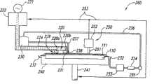
图4是根据本发明的另一个实施方案,包括其位置能够支撑基底110的支架部件240的装置的部分示意性侧视图。在该实施方案的一个方面,支架部件240支撑基底110,使导电层111朝上。如同参考图3时所述,基底驱动单元241可以使支架部件240和基底110移动。第一电极220a和第二电极220b在导电层111的上方,并且与电源221偶联。支架部件224相对于基底110支撑电极220,并且与电极驱动单元223偶联,以大致类似于参考图3时所述的方式使电极220在导电层111的表面上移动。Figure 4 is a partially schematic side view of an apparatus including asupport member 240 positioned to support asubstrate 110 according to another embodiment of the present invention. In one aspect of this embodiment,standoff member 240 supportssubstrate 110 withconductive layer 111 facing upward. As described with reference to FIG. 3 , thesubstrate driving unit 241 may move thecarriage part 240 and thesubstrate 110 . Thefirst electrode 220 a and thesecond electrode 220 b are above theconductive layer 111 and coupled to apower source 221 . Thesupport member 224 supports theelectrode 220 relative to thebase 110 and is coupled to theelectrode driving unit 223 to move theelectrode 220 on the surface of theconductive layer 111 in a manner substantially similar to that described with reference to FIG. 3 .

在图4所示的实施方案的一个方面中,装置260还包括电解质容器230,电解质容器230有一个供给管237,供给管237的开口238的位置靠近电极220。因此,电解质231可以局部置于电极220和导电层111的界面区域239中,不必覆盖整个导电层111。从导电层111除去的电解质231和导电材料流过基底110,收集在电解质容器232中。电解质231和导电材料的混合物可以流入回收设备233,回收设备233从电解质231中脱除大部分导电材料。位于回收设备233下游的过滤器234进一步过滤电解质231,泵235将复原的电解质231通过返回管线236返回电解质容器230。In one aspect of the embodiment shown in FIG. 4 ,device 260 further includes anelectrolyte container 230 having asupply tube 237 with anopening 238 located adjacent toelectrode 220 . Therefore, theelectrolyte 231 may be locally disposed in theinterface region 239 of theelectrode 220 and theconductive layer 111 , without necessarily covering the entireconductive layer 111 . Theelectrolyte 231 and conductive material removed from theconductive layer 111 flows through thesubstrate 110 and collects in theelectrolyte reservoir 232 . The mixture ofelectrolyte 231 and conductive material may flow intorecovery device 233 , which removes most of the conductive material fromelectrolyte 231 . Afilter 234 located downstream of therecovery device 233 further filters theelectrolyte 231 , and apump 235 returns thereconstituted electrolyte 231 to theelectrolyte container 230 through areturn line 236 .

在图4所示的实施方案的另一个方面中,装置260可以包括传感器组件250,该组件具有靠近导电层111的传感器251及与传感器251偶联的用于加工传感器251产生的信号的传感器控制单元252。控制单元252还可以使传感器251相对于基底110移动。在该实施方案的另一方面,传感器组件250以通过反馈线路与电极驱动单223和/或基底驱动单元241偶联。因此,传感器251可以确定导电层111的哪些区域需要进一步脱除材料,并且能够使电极220和/或基底110相对移动,从而将电极220定位在这些区域上。一种替代方案是,(例如,当脱除过程具有高度重复性时),电极220和/或基底110可以根据预定的移动程序相对移动。In another aspect of the embodiment shown in FIG. 4 ,device 260 may include asensor assembly 250 having asensor 251 adjacent toconductive layer 111 and a sensor control coupled tosensor 251 for processing a signal generated bysensor 251 .Unit 252. Thecontrol unit 252 can also move thesensor 251 relative to thesubstrate 110 . In another aspect of this embodiment,sensor assembly 250 is coupled toelectrode drive unit 223 and/orsubstrate drive unit 241 via feedback lines. Thus, thesensor 251 can determine which areas of theconductive layer 111 require further material removal, and can move theelectrode 220 and/or thesubstrate 110 relative to each other to position theelectrode 220 on those areas. Alternatively, (eg, when the stripping process is highly repetitive), theelectrode 220 and/or thesubstrate 110 can be moved relative to each other according to a predetermined movement program.

传感器251和传感器控制单元252可以具有任意数量的合适布置。例如,在一个实施方案中,传感器251可以是光学传感器,当脱除导电材料时,探测基底110反射光的强度、波长或相移的变化。一种替代方案是,传感器251以发射和探测其它波长的射线如X射线的反射。在另一个实施方案中,传感器251可以测量两个选择点之间的导电层111的电阻或电容的变化。在该实施方案的另一方面,一个或两个电极220可以执行传感器251的功能(和上述除去材料的功能),不必使用单独的传感器251。在另一个实施方案中,当脱除导电层111时,传感器251可以探测电源221提供的电压和/或电流的变化。Sensor 251 andsensor control unit 252 may have any number of suitable arrangements. For example, in one embodiment,sensor 251 may be an optical sensor that detects changes in the intensity, wavelength, or phase shift of light reflected fromsubstrate 110 as conductive material is removed. An alternative is for thesensor 251 to emit and detect reflections of other wavelengths of radiation, such as X-rays. In another embodiment,sensor 251 may measure a change in resistance or capacitance ofconductive layer 111 between two selected points. In another aspect of this embodiment, one or bothelectrodes 220 may perform the function of sensor 251 (and the aforementioned material removal function), without the use of aseparate sensor 251 . In another embodiment, thesensor 251 can detect changes in the voltage and/or current provided by thepower source 221 when theconductive layer 111 is removed.

在前面参考图4时所述的任一实施方案中,传感器251都可以远离电解质231,因为电解质231集中在电极220和导电层111的界面区域239中。因此可以改善传感器251探测电解工艺进行的精确度,因为电解质231不大可能影响传感器251的作业。例如,当传感器251是光学传感器时,因为传感器251的位置远离界面区域239,所以电解质231不大可能扭曲基底110表面反射的射线。In either of the embodiments described above with reference to FIG. 4 , thesensor 251 can be remote from theelectrolyte 231 because theelectrolyte 231 is concentrated in theinterface region 239 of theelectrode 220 and theconductive layer 111 . The accuracy with which thesensor 251 detects the progress of the electrolysis process can thus be improved since theelectrolyte 231 is less likely to affect the operation of thesensor 251 . For example, whensensor 251 is an optical sensor,electrolyte 231 is less likely to distort radiation reflected from the surface ofsubstrate 110 becausesensor 251 is located away frominterface region 239 .

前面参考图4时所述的装置260的一个实施方案的另一个特点是用复原的电解质或新鲜的电解质持续补充供给界面区域239的电解质231。这一特点的优点是电极220和导电层111之间的电化学反应能够保持在高而一致的水平上。Another feature of one embodiment of thedevice 260 described above with reference to FIG. 4 is the continuous replenishment of theelectrolyte 231 supplied to theinterface region 239 with reconstituted electrolyte or fresh electrolyte. The advantage of this feature is that the electrochemical reaction between theelectrode 220 and theconductive layer 111 can be maintained at a high and consistent level.

图5是将交流电通过第一种电解质331a和第二种电解质331b导向基底110的装置360的部分示意性侧视图。在该实施方案的一个方面,第一种电解质331a放置在两个第一种电解质容器330a中,第二种电解质331b放置在第二种电解质容器330b中。第一种电解质容器330a部分浸没在第二种电解质331b中。装置360还可以包括电极320,在图中示为第一电极320a和第二电极320b,这两个电极都与电源321偶联,都盛放在第一种电解质容器330a中。一种替代方案是,其中的一个电极320可以与大地偶联。电极320可以包括诸如银、铂、铜和/或其它材料的材料,第一种电解质331a可以包括氯化钠、氯化钾、硫酸铜和/或其它能够和形成电极320的材料相容的电解质。5 is a partially schematic side view of adevice 360 for directing an alternating current to thesubstrate 110 through thefirst electrolyte 331a and thesecond electrolyte 331b. In one aspect of this embodiment,first electrolyte 331a is placed in twofirst electrolyte containers 330a andsecond electrolyte 331b is placed insecond electrolyte container 330b. Thefirst electrolyte container 330a is partially submerged in thesecond electrolyte 331b. Thedevice 360 may also include electrodes 320, shown as afirst electrode 320a and asecond electrode 320b, both coupled to apower source 321 and housed in afirst electrolyte container 330a. As an alternative, one of the electrodes 320 can be coupled to ground. Electrode 320 may include materials such as silver, platinum, copper, and/or other materials, andfirst electrolyte 331a may include sodium chloride, potassium chloride, copper sulfate, and/or other electrolytes that are compatible with the material forming electrode 320 .

在该实施方案的一个方面中,第一种电解质容器330a包括流量限制器322,如用TeflonTM、烧结材料如烧结玻璃、石英或蓝宝石或其它合适的多孔材料制成的渗透性隔离膜,装置膜允许离子在第一种电解质容器330a和第二种电解质容器330b之间进出,不允许第二种电解质330b向里进入电极320(例如,以大致类似于盐桥的方式)。一种替代方案是,第一种电解质331a可以从第一种电解质源339以足以使第一种电解质331a通过流量限制器322向外导出且不允许第一种电解质331a或第二种电解质330b回流到流量限制器322的压力和速度供给电解质容器330a。在任一实施方案中,第一种电解质331a通过限制器322的流动使第二种电解质331b与电极320保持电偶联。In one aspect of this embodiment, thefirst electrolyte container 330a includes aflow restrictor 322, such as a permeable barrier membrane made of Teflon , a sintered material such as sintered glass, quartz or sapphire, or other suitable porous material, device The membrane allows ions to pass in and out between thefirst electrolyte reservoir 330a and thesecond electrolyte reservoir 330b, and does not allow thesecond electrolyte 330b to pass inward into the electrode 320 (eg, in a manner generally similar to a salt bridge). As an alternative, thefirst electrolyte 331a may be directed from thefirst electrolyte source 339 in an amount sufficient to allow thefirst electrolyte 331a to flow outward through theflow restrictor 322 and not allow backflow of thefirst electrolyte 331a or thesecond electrolyte 330b The pressure and velocity to flow restrictor 322feed electrolyte reservoir 330a. In either embodiment, the flow of thefirst electrolyte 331a through therestrictor 322 keeps thesecond electrolyte 331b electrically coupled to the electrode 320 .

在该实施方案的一个方面,装置360还可以包括支撑基底110的支架部件340,导电层111朝向电极320。例如,支架部件340可以放置在第二种电解质容器330b中。在该实施方案的另一方面,支架部件340和/或电极320可以通过一个或多个驱动单元(图中未示出)相互作相对移动。In one aspect of this embodiment, thedevice 360 can also include asupport member 340 supporting thesubstrate 110 with theconductive layer 111 facing the electrode 320 . For example, thestand member 340 may be placed in thesecond electrolyte container 330b. In another aspect of this embodiment, thesupport member 340 and/or the electrodes 320 can be moved relative to each other by one or more drive units (not shown).

前面参考图5时所述的装置360的一个实施方案的一个特点是可以选择第一种电解质331a,使其与电极320相容。这一特点的优点是第一种电解质331a与传统电解质相比对电极320的破坏性小。相反,选择第二种电解质331b时不用考虑其对电极320的影响,因为流量限制器322使其与电极320化学隔离。因此,第二种电解质331b可以包括能够和基底110的导电层111剧烈反应的盐酸或另一种试剂。A feature of one embodiment of thedevice 360 described above with reference to FIG. 5 is that thefirst electrolyte 331a can be selected to be compatible with the electrodes 320. An advantage of this feature is that thefirst electrolyte 331a is less destructive to the electrode 320 than conventional electrolytes. In contrast, thesecond electrolyte 331b is selected without regard to its effect on the electrode 320 because theflow restrictor 322 chemically isolates it from the electrode 320 . Accordingly, thesecond electrolyte 331b may include hydrochloric acid or another reagent capable of violently reacting with theconductive layer 111 of thesubstrate 110 .

图6是根据本发明的几个实施方案放置在多个具有多种形状和结构的电极下面的微电子基底110的顶部平面图。为了演示,图中所示的几个不同类型的电极靠近同一微电子基底110放置;但是,在实际上,同一类型的多个电极可以相对于单个微电子基底110放置。6 is a top plan view of amicroelectronic substrate 110 positioned under a plurality of electrodes having various shapes and configurations according to several embodiments of the present invention. For demonstration purposes, several electrodes of different types are shown positioned adjacent to the samemicroelectronic substrate 110; however, in practice, multiple electrodes of the same type may be positioned relative to a singlemicroelectronic substrate 110.

在一个实施方案中,电极720a和720b可以组成电极对770a,每一个电极720a和720b与电源121的相对端偶联(图3)。电极770a和770b可以具有延长的或条带形状,可以在基底110的直径上相互平行延伸布置。如前面参考图3时所述,可以选择电极对370a的相邻电极之间的间距,使电流导向基底110。In one embodiment,electrodes 720a and 720b may form electrode pair 770a, with eachelectrode 720a and 720b coupled to opposite ends of power source 121 (FIG. 3). Theelectrodes 770 a and 770 b may have an elongated or strip shape, and may be arranged extending parallel to each other on the diameter of thesubstrate 110 . As previously described with reference to FIG. 3 , the spacing between adjacent electrodes of electrode pair 370 a may be selected such that current is directed tosubstrate 110 .

在一个替代性的实施方案中,电极720c和720d可以组成电极对770b,每一个电极720c和720d都可以具有楔或“馅饼”形状,向着微电子基底110的中心方向呈锥形。在另一个实施方案中,条形电极720e和720f可以组成电极对770c,每一个电极720e和720f都从微电子基底110的中心113向微电子基底110的周缘112径向外延。In an alternative embodiment,electrodes 720c and 720d may formelectrode pair 770b, and eachelectrode 720c and 720d may have a wedge or "pie" shape that tapers toward the center ofmicroelectronic substrate 110. In another embodiment, thestrip electrodes 720e and 720f can form anelectrode pair 770c, eachelectrode 720e and 720f extending radially from thecenter 113 of themicroelectronic substrate 110 to theperiphery 112 of themicroelectronic substrate 110.

在另一个实施方案中,单个电极720g可以在大约占微电子基底110一半的面积上延伸,可以具有半圆形平面形状。电极720g可以和具有对应于电极720g镜像形状的另一个电极(图中未示出)组配,这两个电极都可以与电源121偶联,从而以任何一种前面参考图3-5时所述的方式为微电子基底提供交流电。In another embodiment, asingle electrode 720g can extend over approximately half the area of themicroelectronic substrate 110 and can have a semi-circular plan shape.Electrode 720g may be combined with another electrode (not shown) having a mirror-image shape ofelectrode 720g, both of which may be coupled topower source 121 to operate in any of the ways previously described with reference to FIGS. 3-5. The method described above provides alternating current to the microelectronic substrate.

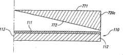
图7是前面参考图6时所述的位于电极720c下面的部分基底110的部分示意性截面侧视图。在该实施方案的一个方面,电极720c具有上表面771和下表面772,下表面772与上表面771对置且面对基底110的导电层111。下表面772可以以该实施方案的一种方式从基底110的中心113向基底110的周缘112向下呈锥形,以使电极720c具有楔形结构。一种替代方案是,电极720c可以具有板形结构,下表面772如图7所示放置,上表面771和下表面772平行。任一实施方案的一个特点是电极720c和基底110之间的朝向基底110的周缘112的电偶联强于朝向基底110的中心113的电偶联。当基底110的周缘112相对于电极720c的移动速度大于基底110的中心113相对于电极720c的移动速度时,例如,当基底110绕其中心113旋转时,这一特点是有利的。因此,电极720c的形状可以说明电极和基底110之间的相对移动。FIG. 7 is a partially schematic cross-sectional side view of the portion ofsubstrate 110underlying electrode 720c described above with reference to FIG. 6 . In one aspect of this embodiment, theelectrode 720c has anupper surface 771 and alower surface 772 opposite theupper surface 771 and facing theconductive layer 111 of thesubstrate 110 . Thelower surface 772 may taper downwardly from thecenter 113 of the base 110 toward theperiphery 112 of the base 110 in one manner of this embodiment so that theelectrode 720c has a wedge-shaped configuration. As an alternative, theelectrode 720c may have a plate-shaped structure, thelower surface 772 is placed as shown in FIG. 7 , and theupper surface 771 and thelower surface 772 are parallel. It is a feature of either embodiment that the electrical coupling between theelectrode 720c and thesubstrate 110 is stronger toward theperiphery 112 of thesubstrate 110 than toward thecenter 113 of thesubstrate 110 . This feature is advantageous when theperipheral edge 112 of thesubstrate 110 moves faster relative to theelectrode 720c than thecenter 113 of thesubstrate 110 relative to theelectrode 720c, eg, when thesubstrate 110 rotates about itscenter 113 . Thus, the shape of theelectrode 720c can account for the relative movement between the electrode and thesubstrate 110 .

在其它实施方案中,电极720c可以具有其它形状。In other embodiments,electrode 720c may have other shapes.

例如,下表面772可以是曲面,不是平面。For example,lower surface 772 may be curved rather than flat.

一种替代方案是,前面参考图6所述的任意电极(或者其形状不是图6所示那些形状的其它电极)都可以具有倾斜或弯曲的下表面。在另一个实施方案中,电极可以具有用于说明电极和基底110之间的相对移动的形状。Alternatively, any of the electrodes described above with reference to Figure 6 (or other electrodes having shapes other than those shown in Figure 6) may have a sloped or curved lower surface. In another embodiment, the electrodes may have shapes to account for relative movement between the electrodes and thesubstrate 110 .

图8A是根据本发明的另一个实施方案用于支撑多个电极的电极支架473的部分示意图。在该实施方案的一个方面,电极支架473可以包括多个电极孔474,每一个电极孔474盛放第一电极420a或第二电极420b。第一电极420a通过孔474与第一导线428a偶联,第二电极420b与第二导线428b偶联。第一导线428a与第二导线428b都与电源421偶联。因此,第一电极420a和第二电极420b的每一个电极对470都定义了部分由前面参考图3-5时所述的基底110和电解质完成的电路。8A is a partial schematic diagram of anelectrode holder 473 for supporting multiple electrodes according to another embodiment of the present invention. In one aspect of this embodiment, theelectrode holder 473 may include a plurality of electrode holes 474, eachelectrode hole 474 receiving the first electrode 420a or thesecond electrode 420b. The first electrode 420a is coupled to thefirst wire 428a through thehole 474, and thesecond electrode 420b is coupled to thesecond wire 428b. Both thefirst wire 428 a and thesecond wire 428 b are coupled to thepower source 421 . Thus, eachelectrode pair 470 of the first electrode 420a and thesecond electrode 420b defines an electrical circuit partially completed by thesubstrate 110 and electrolyte as previously described with reference to FIGS. 3-5.

在该实施方案的一个方面,第一导线428a与第二导线428b可以有一定的偏移,以降低导线之间短路和/或电容耦合的可能性。在该实施方案的另一方面,电极支架473可以具有大致类似于前面参考图1-7时所述的那些结构中的任意一种结构。例如,前面参考图6时所述的任一电极(如320a、320c、320e或320g)都可被具有相同的整体形状且包括多个盛放多个第一电极420a或多个第二电极420b之一的孔474的电极支架473代替。In one aspect of this embodiment, thefirst lead 428a can be offset from thesecond lead 428b to reduce the possibility of shorting and/or capacitive coupling between the leads. In another aspect of this embodiment, theelectrode holder 473 can have a structure substantially similar to any of those previously described with reference to FIGS. 1-7. For example, any of the electrodes (such as 320a, 320c, 320e, or 320g) described above with reference to FIG. One of theholes 474 is replaced by theelectrode holder 473 .

在该实施方案的另一方面,图8A所示的电极对470可以以对应于电极420a、420b和微电子基底110之间的接近度布置(图7),和/或电极对470可以对应于电极420a、420b和微电子基底110之间的相对移动速度布置。例如,电极对470可以更集中在基底110的周缘112或电极对470和基底110之间的相对速度较高的其它区域中(见图7)。因此,电极对470浓度的增加能够提高电解电流,以补偿较高的速度。另外,每一个电极对470的第一电极420a和第二电极420b可以一起相对靠近电极靠近导电层111(见图7)的区域中(如:基底110的周缘112),因为靠近导电层111可以降低第一电极420a和第二电极420b之间直接电耦合的可能性。在该实施方案的另一方面,供给不同电极对470的振幅、频率和/或波形可以随诸如电极对470和微电子基底110的间距及电极对470和微电子基底110的相对速度的因素而变化。In another aspect of this embodiment, theelectrode pair 470 shown in FIG. 8A can be arranged in a corresponding proximity between theelectrodes 420a, 420b and the microelectronic substrate 110 ( FIG. 7 ), and/or theelectrode pair 470 can correspond to The relative speed of movement between theelectrodes 420a, 420b and themicroelectronic substrate 110 is arranged. For example, electrode pairs 470 may be more concentrated inperimeter 112 ofsubstrate 110 or other areas where the relative velocity between electrode pairs 470 andsubstrate 110 is high (see FIG. 7 ). Thus, an increase in the concentration of theelectrode pair 470 can increase the electrolysis current to compensate for the higher speed. In addition, the first electrode 420a and thesecond electrode 420b of eachelectrode pair 470 can be relatively close to the region (such as: theperiphery 112 of the substrate 110) close to the conductive layer 111 (see FIG. 7 ), because theconductive layer 111 can The possibility of direct electrical coupling between the first electrode 420a and thesecond electrode 420b is reduced. In another aspect of this embodiment, the amplitude, frequency, and/or waveform supplied to the various electrode pairs 470 can vary with factors such as the spacing between the electrode pairs 470 and themicroelectronic substrate 110 and the relative velocity of the electrode pairs 470 and themicroelectronic substrate 110. Variety.

图8B和8C示出根据本发明的另一个实施方案同心布置的电极820(在图中示为第一电极820a和第二电极820b)。在图8B所示的一个实施方案中,第一电极820a绕第二电极820b同心布置,可以在第一电极820a和第二电极820b之间放置介电材料829。如图8B所示,第一电极820a可以绕第二电极820b定义全360°的圆弧,或者,第一电极820a也可以定义小于360°的圆弧。8B and 8C illustrate concentrically arranged electrodes 820 (shown asfirst electrode 820a andsecond electrode 820b in the figures) according to another embodiment of the invention. In one embodiment shown in FIG. 8B, afirst electrode 820a is concentrically disposed about asecond electrode 820b, and adielectric material 829 may be placed between thefirst electrode 820a and thesecond electrode 820b. As shown in FIG. 8B, thefirst electrode 820a may define a full 360° arc around thesecond electrode 820b, or thefirst electrode 820a may also define a less than 360° arc.

在另一个实施方案中,如图8C所示,第一电极820a可以在两个第二电极820b之间同心放置,在两个相邻电极820之间放置介电材料829。在该实施方案的一个方面,电流可以没有相移地供给每一个第二电极820b。一种替代方案是,供给一个第二电极820b的电流可以相对于供给其它第二电极820b的电流有相移。在该实施方案的另一方面,供给每一个第二电极820b的电流可以具有不同的不是相位的特征如振幅。In another embodiment, as shown in FIG. 8C , afirst electrode 820a may be placed concentrically between twosecond electrodes 820b with adielectric material 829 placed between two adjacent electrodes 820 . In one aspect of this embodiment, current may be supplied to eachsecond electrode 820b without a phase shift. As an alternative, the current supplied to onesecond electrode 820b may be phase shifted relative to the current supplied to the othersecond electrodes 820b. In another aspect of this embodiment, the current supplied to eachsecond electrode 820b may have a different characteristic other than phase, such as amplitude.

前面参考图8B和8C时所述的电极820的一个特点是第一电极820a能够屏蔽第二电极820b,使其免受其它电源的干扰。例如,第一电极820a可以与大地偶联,以屏蔽第二电极820b。这一布置的优点是能够更精确地控制通过电极820供给基底110的电流(图7)。One feature of the electrode 820 described above with reference to FIGS. 8B and 8C is that thefirst electrode 820a can shield thesecond electrode 820b from interference from other power sources. For example, thefirst electrode 820a may be coupled to ground to shield thesecond electrode 820b. An advantage of this arrangement is the ability to more precisely control the current supplied to thesubstrate 110 through the electrodes 820 (FIG. 7).

图9是根据本发明的一个实施方案用于化学、机械和/或电解加工微电子基底110的装置560的示意图。在该实施方案的一个方面,在放置抛光垫582的操作部分“W”的一个工作站处,装置560具有带有顶板581的支撑台580。顶板581一般是一个刚性板,在脱除材料过程中提供一个将抛光垫582的特定部位固定在其上的平整固体表面。Figure 9 is a schematic illustration of anapparatus 560 for chemically, mechanically and/or electrolyticallyprocessing microelectronic substrate 110 according to one embodiment of the present invention. In one aspect of this embodiment, theapparatus 560 has a support table 580 with atop plate 581 at a station where the operative portion "W" of thepolishing pad 582 is placed.Top plate 581 is generally a rigid plate that provides a flat solid surface on which to secure a specific portion of polishingpad 582 during material removal.

装置560还可以具有多个辊,用于在顶板581上导引、定位和夹持抛光垫582。这些辊可以包括供料辊583、第一和第二托辊584a和584b、第一和第二导辊585a和585b及拉紧辊586。供料辊583承载抛光垫582的未使用或预操作部分,拉紧辊583承载抛光垫582的使用或后操作部分。另外,第一托辊584a和第一导辊585a可以在顶板581上张紧抛光垫582,使抛光垫582在操作过程中保持静止。马达(图中未示出)驱动至少一个供料辊583和拉紧辊586,使抛光垫582连续通过顶板581。因此,抛光垫582的清洁的预操作部分很快就替换使用过的部分,为抛光和/或清洁基底110提供一致的表面。Apparatus 560 may also have a plurality of rollers for guiding, positioning and clampingpolishing pad 582 ontop plate 581 . These rolls may include afeed roll 583 , first and second idler rolls 584 a and 584 b , first and second guide rolls 585 a and 585 b , and a take-up roll 586 .Supply roll 583 carries the unused or pre-operated portion of polishingpad 582 and take-up roll 583 carries the used or post-operated portion of polishingpad 582 . In addition, thefirst idler roller 584a and thefirst guide roller 585a can tension thepolishing pad 582 on thetop plate 581 so that thepolishing pad 582 remains stationary during operation. A motor (not shown in the figure) drives at least onefeed roller 583 and take-uproller 586 to make thepolishing pad 582 pass through thetop plate 581 continuously. Thus, the cleaned pre-operated portion of thepolishing pad 582 quickly replaces the used portion, providing a consistent surface for polishing and/or cleaning thesubstrate 110 .

装置560还可以具有在脱除材料过程中能够控制和保护基底110的托架组件590。Apparatus 560 may also have acarriage assembly 590 that enables control and protection ofsubstrate 110 during material removal.

托架组件590可以包括基底夹具592,在脱除材料的适当阶段提取、夹持和释放基底110。托架组件590还可以具有支撑龙门架594,支撑龙门架594承载驱动组件595,驱动组件595可以沿龙门架594平移。驱动组件595可以具有传动器596、与传动器596偶联的主动轴597和从主动轴597伸出的臂598。臂598通过端轴599承载基底夹具592,驱动组件595使基底夹具592绕轴E-E转动(箭头“R1”所示)。端轴599还可以使基底夹具592绕其中心轴F-F转动(箭头“R2”所示)。Thecarriage assembly 590 may include a substrate gripper 592 to extract, hold and release thesubstrate 110 at appropriate stages of material removal. Thecarriage assembly 590 may also have asupport gantry 594 carrying adrive assembly 595 that may translate along thegantry 594 .Drive assembly 595 may have atransmission 596 , adrive shaft 597 coupled totransmission 596 , and anarm 598 extending fromdrive shaft 597 . Arm 598 carries substrate holder 592 via end shaft 599, and driveassembly 595 rotates substrate holder 592 about axis EE (shown by arrow "R1 "). End shaft 599 also allows rotation of substrate holder 592 about its central axis FF (shown by arrow "R2 ").

在一个实施方案中,抛光垫582和平整溶液587至少定义了一部分用于从基底110表面上机械和/或化学-机械脱除材料的材料脱除介质。装置560中使用的抛光垫582可以是固定磨料抛光垫,其中的磨料颗粒固定粘结在悬浮介质上。因此,平整溶液587可以是没有磨料颗粒的“清洁溶液”,因为磨料颗粒固定地分布在抛光垫582的抛光表面588上。In one embodiment, polishingpad 582 andplanarization solution 587 define at least a portion of a material removal medium for mechanical and/or chemical-mechanical removal of material from the surface ofsubstrate 110 .Polishing pad 582 used inapparatus 560 may be a fixed abrasive polishing pad in which abrasive particles are fixedly bonded to a suspending medium. Thus, theleveling solution 587 may be a “cleaning solution” without abrasive particles because the abrasive particles are fixedly distributed on the polishingsurface 588 of thepolishing pad 582 .

在其它领域,抛光垫582可以是没有磨料颗粒的无磨料垫,平整溶液587可以是具有能够从基底110中脱除材料的磨料颗粒和化学物质的浆液。在其它领域,抛光垫582和平整溶液587都设计为没有磨料颗粒或元素,这将在下面参考图9-11详述。In other areas, polishingpad 582 may be a non-abrasive pad without abrasive grains, and levelingsolution 587 may be a slurry with abrasive grains and chemicals capable of removing material fromsubstrate 110 . In other areas, both thepolishing pad 582 and theleveling solution 587 are designed without abrasive particles or elements, as will be described in more detail below with reference to FIGS. 9-11.

为了用装置560从基底110中除去材料,托架组件590在有平整溶液587存在的情况下使基底110的面113贴紧抛光垫582的抛光面588。然后,驱动组件595使基底夹具592绕轴E-E转动,并且任选地使基底夹具592绕轴F-F转动,使基底110平移通过抛光面588。结果在化学和/或化学-机械平整(CMP)工艺中,材料脱除介质中的磨料颗粒和/或化学物质从基底110的表面上脱除材料。因此,在一个实施方案中,抛光垫582通过去除基底110的导电层111上突出的粗糙体而平整基底110。To remove material fromsubstrate 110 withapparatus 560 ,carriage assembly 590 bringsface 113 ofsubstrate 110 against polishingsurface 588 of polishingpad 582 in the presence of levelingsolution 587 . Drive assembly 595 then rotates substrate holder 592 about axis E-E, and optionally rotates substrate holder 592 about axis F-F, to translatesubstrate 110 across polishingsurface 588 . As a result, the abrasive particles and/or chemicals in the material removal media remove material from the surface of thesubstrate 110 in a chemical and/or chemical-mechanical planarization (CMP) process. Thus, in one embodiment, polishingpad 582planarizes substrate 110 by removing asperities protruding fromconductive layer 111 ofsubstrate 110 .

在该实施方案的另一方面,装置560可以包括电解质供应容器530,用导管537将电解质释放到抛光垫582的抛光面588上,这将在下面参考图10时详述。装置560还可以包括与支撑台580和/或顶板581偶联的电源521,向位于支撑台580和/或顶板581中的电极供应电流。因此,装置560可以以类似于前面参考图1-8C时所述的方式从导电层111中电解脱除材料。In another aspect of this embodiment,apparatus 560 may include anelectrolyte supply reservoir 530 withconduit 537 to discharge electrolyte onto polishingsurface 588 of polishingpad 582, as will be described in more detail below with reference to FIG. 10 .Apparatus 560 may also include apower source 521 coupled to support table 580 and/ortop plate 581 to supply current to electrodes located in support table 580 and/ortop plate 581 . Accordingly,device 560 may electrolytically remove material fromconductive layer 111 in a manner similar to that previously described with reference to FIGS. 1-8C.

在前面参考图9时所述的装置560的一个实施方案的一个方面中,可以先用电解法再用CMP法相继从基底110的导电层111中除去材料。例如,电解法可以以糙化导电层111的方式从导电层111中除去材料。选定的电解时间过后,停止电解操作,利用CMP法脱除其它材料。电解法和CMP法也可以同时进行。在任何一种这样的安排中,前面参考图9时所述的装置560的一个实施方案的一个特点是同一个装置560可以利用CMP平整基底110和利用电解法从基底110中脱除材料。该布置的一个优点是基底110不需要从一个装置移动到另一个装置进行CMP和电解工艺。In one aspect of one embodiment ofapparatus 560 described above with reference to FIG. 9, material may be removed fromconductive layer 111 ofsubstrate 110 sequentially by electrolysis followed by CMP. For example, electrolysis may remove material fromconductive layer 111 in a manner that roughensconductive layer 111 . After the selected electrolysis time has elapsed, the electrolysis operation is stopped and other materials are removed by CMP. Electrolysis and CMP can also be performed simultaneously. In either such arrangement, a feature of one embodiment of theapparatus 560 described above with reference to FIG. 9 is that thesame apparatus 560 can planarize thesubstrate 110 by CMP and remove material from thesubstrate 110 by electrolysis. One advantage of this arrangement is that thesubstrate 110 does not need to be moved from one device to another for the CMP and electrolysis processes.

前面参考图9时所述的装置560的一个实施方案的另一个优点是这些工艺相互结合使用时有望比一些传统工艺更快速和精确地从基底110中除去材料。例如,如上所述,电解法可以以糙化微电子基底110的方式除去大量材料,平整法以平整和/或平滑微电子基底110的方式更精细地脱除材料。Another advantage of an embodiment ofapparatus 560 described above with reference to FIG. 9 is that these processes, when used in conjunction with each other, are expected to remove material fromsubstrate 110 more rapidly and accurately than some conventional processes. For example, as described above, electrolysis may remove substantial amounts of material in a manner that roughensmicroelectronic substrate 110 , and planarization may remove material in a manner that flattens and/or smoothesmicroelectronic substrate 110 in a finer manner.

图10是参考图9时所述的装置560的一部分的部分示意性的分解轴测图。在图10所示实施方案的一个方面,顶板581盛放多个每个都包括第一电极520a和第二电极520b的电极对570。第一电极520a与第一导线528a偶联,第二电极520b与第二导线528b偶联。第一导线528a与第二导线528b都与电源521偶联(图9)。在该实施方案的一个方面,可以用包括TeflonTM或其它合适的介电材料的电极介电层529a将第一电极520a和第二电极520b隔开。因此,电极介电层529a可以控制第一电极520a和第二电极520b之间区域的体积和介电常数,从而能够控制电极之间的耦合。FIG. 10 is a partially schematic exploded isometric view of a portion of thedevice 560 described with reference to FIG. 9 . In one aspect of the embodiment shown in FIG. 10, thetop plate 581 holds a plurality of electrode pairs 570 each including afirst electrode 520a and asecond electrode 520b. Thefirst electrode 520a is coupled to afirst wire 528a, and thesecond electrode 520b is coupled to asecond wire 528b. Both thefirst wire 528a and thesecond wire 528b are coupled to the power source 521 ( FIG. 9 ). In one aspect of this embodiment, thefirst electrode 520a and thesecond electrode 520b may be separated by an electrode dielectric layer 529a comprising Teflon or other suitable dielectric material. Therefore, the electrode dielectric layer 529a can control the volume and dielectric constant of the region between thefirst electrode 520a and thesecond electrode 520b, thereby enabling control of coupling between the electrodes.

电极520a和520b可以通过抛光垫582与微电子基底110电偶联(图9)。在该实施方案的一个方面,供料导管537通过就在抛光垫582下面的顶板581中的孔538供应的电解质531使抛光垫582饱和。因此选择的电极520a和520b与电解质531相容。在一个替代性的布置中,电解质531可以从上面(例如将电解质531放置在平整液587中)而不是通过顶板581供给抛光垫582。因此,抛光垫582可以包括放置在抛光垫582与电极520a和520b之间的垫介电层529b。当垫介电层529b处在适当位置时,电极520a和520b与电解质531物理接触隔离,因此可以选自与电解质531不相容的材料。在任一实施方案中,电极520a和520b相互之间及与导电层111之间通过电解质531的普通体积流体连通。每一个电极520a、520b都可以比其它电极更直接地与导电层111电偶联(图9),使得电流从一个电极通过导电层111流向其它电极。Electrodes 520a and 520b may be electrically coupled tomicroelectronic substrate 110 through polishing pad 582 (FIG. 9). In one aspect of this embodiment, polishingpad 582 is saturated withelectrolyte 531 supplied byfeed conduit 537 through aperture 538 intop plate 581 just below polishingpad 582 .Electrodes 520a and 520b are thus selected to be compatible withelectrolyte 531 . In an alternative arrangement,electrolyte 531 may be supplied to polishingpad 582 from above (eg, by placingelectrolyte 531 in leveling fluid 587 ) rather than throughtop plate 581 . Accordingly, polishingpad 582 may include pad dielectric layer 529b disposed betweenpolishing pad 582 andelectrodes 520a and 520b. When pad dielectric layer 529b is in place,electrodes 520a and 520b are isolated from physical contact withelectrolyte 531 and thus may be selected from materials that are incompatible withelectrolyte 531 . In either embodiment,electrodes 520a and 520b are in fluid communication with each other and withconductive layer 111 through the common volume ofelectrolyte 531 . Eachelectrode 520a, 520b may be more directly electrically coupled to theconductive layer 111 than the other electrodes (FIG. 9), so that current flows from one electrode through theconductive layer 111 to the other electrode.

在图10所示装置的一个实施方案的一个方面中,电极520a和520b面向微电子基底110的工作面113(图9),抛光垫582插在电极520a和520b与工作面113之间。当微电子基底110与电极520a和520b相对移动时,电极至少要和大部分工作面113电偶联。因此,与传统的设备相比,在工作面113处在导电层111(图9)中形成电隔离“岛”的可能性降低。一种替代方案是,如果装置只包括两个电极,且每一个都设计为面向约半面工作面113(其方式大致类似于前面参考图6的电极220g时所述),则电极也可以至少与大部分工作面113电偶联。In one aspect of one embodiment of the apparatus shown in FIG. 10 ,electrodes 520 a and 520 b face working surface 113 ( FIG. 9 ) ofmicroelectronic substrate 110 , and polishingpad 582 is interposed betweenelectrodes 520 a and 520 b and workingsurface 113 . Theelectrodes 520a and 520b are electrically coupled to at least a majority of the workingsurface 113 when themicroelectronic substrate 110 moves relative to theelectrodes 520a and 520b. Thus, the likelihood of electrically isolated "islands" forming in the conductive layer 111 (FIG. 9) at the workingface 113 is reduced compared to conventional devices. One alternative is that if the device comprises only two electrodes, each of which is designed to face approximately half of the working surface 113 (in a manner substantially similar to that described above with reference to electrode 220g of FIG. Most of the workingsurfaces 113 are electrically coupled.

在参考图10所述的任意一个实施方案中,抛光垫582与一些传统电解装置相比有几个额外的优点。例如,抛光垫582可以将电极520a和520b与微电子基底110(图9)均匀分开,这样可以提高用电解法从导电层111(图9)中除去材料的均匀性。抛光垫582还可以具有能够以前面参考图9时所述的方式平整微电子基底110的磨料颗粒589。另外,抛光垫582可以从电极520a和520b中滤去炭或其它腐蚀材料,以防止电极材料接触微电子基底110。另外,抛光垫582可以作为海绵将电解质531保持在靠近微电子基底110的位置上。In either of the embodiments described with reference to FIG. 10, thepolishing pad 582 has several additional advantages over some conventional electrolysis devices. For example, polishingpad 582 can evenlyseparate electrodes 520a and 520b from microelectronic substrate 110 (FIG. 9), which can improve the uniformity of electrolytic removal of material from conductive layer 111 (FIG. 9).Polishing pad 582 may also have abrasive particles 589 capable of planarizingmicroelectronic substrate 110 in the manner previously described with reference to FIG. 9 . Additionally, polishingpad 582 may filter carbon or other corrosive materials fromelectrodes 520a and 520b to prevent electrode material from contactingmicroelectronic substrate 110 . Additionally, polishingpad 582 may act as a sponge to holdelectrolyte 531 in close proximity tomicroelectronic substrate 110 .

图11是根据本发明的另一个实施方案机械、化学和/或电解加工微电子基底110的旋转装置660的部分示意性截面侧视图。在该实施方案的一个方面,装置660具有大致是圆形的台板或台面680、托架组件690、在台面680上的抛光垫682和抛光垫682上的平整液687。抛光垫682可以是固定磨料抛光垫,或者,平整液687可以是悬浮有磨料元素的浆液,而抛光垫682可以是无磨料垫。在平整期间,驱动组件695旋转(箭头“G”)和/或往复移动(箭头“H”)台板680,以移动抛光垫682。Figure 11 is a partially schematic cross-sectional side view of arotating apparatus 660 for mechanically, chemically and/or electrolytically machining amicroelectronic substrate 110 according to another embodiment of the present invention. In one aspect of this embodiment,apparatus 660 has a generally circular platen or top 680 , acarriage assembly 690 , apolishing pad 682 on top 680 , and a levelingfluid 687 on polishingpad 682 .Polishing pad 682 may be a fixed abrasive polishing pad, or, levelingfluid 687 may be a slurry with abrasive elements suspended and polishingpad 682 may be a non-abrasive pad. During planarization,drive assembly 695 rotates (arrow “G”) and/or reciprocates (arrow “H”) platen 680 to move polishingpad 682 .

因此,微电子基底110相对于抛光垫682的移动可以包括圆、椭圆、轨道、岁差(precessional)或非岁差移动。Accordingly, movement of themicroelectronic substrate 110 relative to thepolishing pad 682 may include circular, elliptical, orbital, precessional, or non-precessional movement.

从脱除材料过程中托架组件690控制和保护微电子基底110。托架组件690一般具有基底夹具692,垫694利用吸力夹持微电子基底110。托架组件690的驱动组件696一般旋转和/或平移基底夹具692(分别用箭头“I”和“J”表示)。一种替代方案是,基底夹具692可以包括能够在抛光垫682上滑动的自由浮动的重盘(图中未示出)。Carriage assembly 690 controls and protectsmicroelectronic substrate 110 from the material removal process. Thecarrier assembly 690 generally has asubstrate gripper 692 withpads 694 that grip themicroelectronic substrate 110 using suction. Drive assembly 696 ofcarriage assembly 690 generally rotates and/or translates substrate holder 692 (indicated by arrows "I" and "J", respectively). Alternatively, thesubstrate holder 692 may include a free-floating weight plate (not shown) that can slide over thepolishing pad 682 .

为了用一个实施方案的装置660平整微电子基底110,托架组件690使微电子基底110贴紧抛光垫682的抛光面688。然后,台板680和/或基底夹具692相对移动,使微电子基底110平移通过抛光面688。结果,抛光垫682中的磨料颗粒和/或平整液687中的化学物质从微电子基底110的表面上脱除材料。To planarizemicroelectronic substrate 110 withapparatus 660 of one embodiment,carriage assembly 690 holdsmicroelectronic substrate 110 against polishingsurface 688 of polishingpad 682 . Theplaten 680 and/orsubstrate holder 692 are then moved relative to each other to translate themicroelectronic substrate 110 across the polishingsurface 688 . As a result, the abrasive particles in polishingpad 682 and/or the chemicals in smoothingfluid 687 remove material from the surface ofmicroelectronic substrate 110 .

装置660还可以包括电源621,导线628a和628b与一个或多个电极对670偶联(其中的一个示于图11)。电极对670可以大致以与电极520a和520b(图10)与顶板581(图10)整合的同样方式和台板680整合。电极对670也可以和抛光垫682整合。在任意一个实施方案中,电极对670都可以包括其形状和结构大致类似于前面参考图3-10时所述的那些形状和结构的电极,以从微电子基底110中电解除去导电材料。如图前面参考图9时所述,电解工艺可以在CMP工艺前、过程中或之后进行。Apparatus 660 may also include apower source 621, withleads 628a and 628b coupled to one or more electrode pairs 670 (one of which is shown in FIG. 11).Electrode pair 670 may be integrated withplaten 680 in substantially the same manner aselectrodes 520a and 520b (FIG. 10) are integrated with top plate 581 (FIG. 10).Electrode pair 670 may also be integrated withpolishing pad 682 . In either embodiment,electrode pair 670 may include electrodes having shapes and configurations substantially similar to those described above with reference to FIGS. 3-10 to electrolytically remove conductive material frommicroelectronic substrate 110 . As previously described with reference to FIG. 9, the electrolysis process may be performed before, during or after the CMP process.

在本发明的其它实施方案中,可以根据其它方法使用前面参考图3-11时所述的装置。例如,电解工艺可以和直接化学反应一起或取代直接化学反应将微电子基底110的导电部分(包括半导电部分)氧化。在该实施方案的一个方面,电解工艺可以将一般难以或实际上几乎不可能氧化的金属(如铂、铑、铱或金)氧化。该布置的一个优点是可以使这些金属更能实际应用于微电子领域。例如,在不利用均质刻蚀化学品(即,在所有方向上没有偏差刻蚀的化学品)和/或不用抛光垫682对微电子基底施加非常高下挫力的情况下一般难以从微电子基底110中除去铂和其它抗氧化的贵金属。电解工艺可以在大致垂直于抛光垫682的抛光面688的方向上各向异性地氧化铂(或其它导电材料)。In other embodiments of the invention, the devices described above with reference to Figures 3-11 may be used according to other methods. For example, an electrolytic process may oxidize conductive portions (including semiconductive portions) ofmicroelectronic substrate 110 along with or instead of direct chemical reactions. In one aspect of this embodiment, the electrolytic process can oxidize metals that are generally difficult or virtually impossible to oxidize, such as platinum, rhodium, iridium, or gold. An advantage of this arrangement is that it can make these metals more practical for use in microelectronics. For example, it is generally difficult to extract from a microelectronic substrate without utilizing a homogeneous etch chemistry (i.e., a chemistry that etches without deviation in all directions) and/or without thepolishing pad 682 applying very high drag forces to the microelectronic substrate. Platinum and other oxidation-resistant noble metals are removed fromsubstrate 110 . The electrolytic process may anisotropically oxidize platinum (or other conductive material) in a direction generally perpendicular to polishingsurface 688 of polishingpad 682 .

一旦将导电材料氧化,则可以从微电子基底110中将其除去。例如,可以认为电解氧化工艺糙化了导电材料的表面,只在表面下渗透了很短的距离。然后可以通过与抛光垫的化学和/或机械反应和/或平整溶液将氧化后的材料除去。另外,除去氧化材料需要的下挫力小于不包括电解工艺的技术所需要的下挫力。在一个具体例子中已经测定,用本发明的一个实施方案在10分钟内就可以用约0.2psi的压力除去1000埃的铂,用传统的CMP技术一般不可能以这样的速度各向异性地除去铂。一种替代方案是,前面参考图9-11时所述的装置与传统CMP装置相比,可以以更快的速度和/或更小的下挫力氧化和除去非铂的材料。Once the conductive material is oxidized, it can be removed from themicroelectronic substrate 110 . For example, the electrolytic oxidation process can be thought of as roughening the surface of conductive materials, penetrating only a short distance below the surface. The oxidized material can then be removed by chemical and/or mechanical reaction with the polishing pad and/or a leveling solution. Additionally, the downward force required to remove oxidized material is less than that required for techniques that do not include electrolytic processes. In one specific example, it has been determined that 1000 angstroms of platinum can be removed in 10 minutes using an embodiment of the present invention at a pressure of about 0.2 psi, anisotropic removal at such a rate is generally not possible with conventional CMP techniques platinum. As an alternative, the apparatus described above with reference to FIGS. 9-11 can oxidize and remove non-platinum materials at a faster rate and/or with less drag than conventional CMP apparatus.

从微电子基底110中氧化和脱除导电材料的速度的提高的一个优点是与传统技术相比微电子基底110的产率提高。从微电子基底110中各向异性地氧化和除去导电材料的一个优点是不在侧向掏蚀邻近结构的情况下可以除去导电材料的覆盖层。One advantage of the increased speed of oxidation and stripping of conductive material frommicroelectronic substrates 110 is the increased yield ofmicroelectronic substrates 110 compared to conventional techniques. One advantage of anisotropically oxidizing and removing conductive material frommicroelectronic substrate 110 is that an overlying layer of conductive material can be removed without undercutting adjacent structures.

因此,本发明的这些实施方案的方法可以更可靠地在微电子基底110中形成通路、导线和其它导电结构。在加工过程中降低施加于微电子基底110上的下挫力的一个优点是该技术可以降低破坏微电子基底110的可能性,从而可以提高施加下挫力的装置的寿命。Accordingly, the methods of these embodiments of the invention may more reliably form vias, wires, and other conductive structures in themicroelectronic substrate 110 . One advantage of reducing the droop force applied to themicroelectronic substrate 110 during processing is that this technique can reduce the likelihood of damage to themicroelectronic substrate 110, which can increase the life of the device that applies the droop force.

在本发明的另一个实施方案的方法中,可以选择施加于微电子基底110的电信号的性能,用于控制从微电子基底110中除去材料的速度和/或方式。例如,可以增加电流的振幅,以提高导电材料的氧化速度,从而可以提高除去氧化后材料的速度。一种替代方案是,可以减小电流的振幅,以降低氧化速度。In the method of another embodiment of the present invention, the nature of the electrical signal applied to themicroelectronic substrate 110 may be selected for controlling the rate and/or manner in which material is removed from themicroelectronic substrate 110 . For example, the amplitude of the current can be increased to increase the rate of oxidation of the conductive material, thereby increasing the rate of removal of the oxidized material. As an alternative, the amplitude of the current can be reduced to reduce the rate of oxidation.

在另一个实施方案中,可以终止电流,以控制从微电子基底110中除去导电材料的速度。例如,如果电流终止后仍然在进行机械和/或化学脱除材料,则电流的终止能够减慢但不会停止材料的除去速度。一种替代方案是,如果不可能进行机械脱除和/或各向异性化学脱除(例如,当材料包括铂时),则终止施加于导电材料上的电流将停止材料的脱除。在任意一种实施方案中,根据所需的氧化和脱除速度及从微电子基底110中除去材料的种类,电流的振幅可以在约1amp至约10amp的范围内变化。In another embodiment, the current flow can be terminated to control the rate at which the conductive material is removed from themicroelectronic substrate 110 . For example, if mechanical and/or chemical material removal is still ongoing after the current is terminated, the termination of the current can slow but not stop the rate of material removal. As an alternative, if mechanical and/or anisotropic chemical removal is not possible (eg, when the material includes platinum), terminating the application of the current to the conductive material will stop the removal of the material. In either embodiment, the amplitude of the current can vary from about 1 amp to about 10 amps, depending on the desired rate of oxidation and stripping and the type of material being removed from themicroelectronic substrate 110 .

在另一个实施方案中,可以控制的电信号的其它性能,用于控制材料的氧化和脱除速度。例如,可以增加或降低施加于材料上的电压以分别增加或降低材料的氧化和脱除速度。在一个实施方案中,电压最高可变化到约100伏。在另一个实施方案中,可以改变施加的电信号的频率,以控制材料的氧化和脱除速度。在一个具体实施方案中,在用抛光垫582咬合微电子基底110的同时在微电子基底的铂层上施加频率约为60Hz的约10伏的电势,以从微电子基底110中各向异性地除去部分铂。In another embodiment, other properties of the electrical signal that can be controlled are used to control the rate of oxidation and removal of the material. For example, the voltage applied to the material can be increased or decreased to increase or decrease the rate of oxidation and removal of the material, respectively. In one embodiment, the voltage can vary up to about 100 volts. In another embodiment, the frequency of the applied electrical signal can be varied to control the rate of oxidation and removal of the material. In one specific embodiment, a potential of about 10 volts at a frequency of about 60 Hz is applied to the platinum layer of themicroelectronic substrate 110 while engaging thepolishing pad 582 to anisotropically remove Remove some of the platinum.

在任一上述实施方案中,抛光垫582可以是传统垫,如IC 1000抛光垫(可购自Rodell,Inc.of Phoenix,Arizona)。在该实施方案的一个方面,抛光垫582可具有固定分布在悬浮介质中的磨料元素。In any of the above embodiments, thepolishing pad 582 can be a conventional pad, such as the IC 1000 polishing pad (available from Rodell, Inc. of Phoenix, Arizona). In one aspect of this embodiment, polishingpad 582 may have abrasive elements fixedly distributed in the suspending medium.

一种替代方案是,磨料元素可以悬浮在平整液或浆液中,平整液或浆液放置在抛光垫582和微电子基底110之间。在任一实施方案中,磨料元素可以包括二氧化铬、氧化铝或二氧化硅,平整液可以包括电解质,以使微电子基底与电源偶联。在另一个实施方案中,作为电解工艺和与抛光垫582接触的结果是可以从材料脱除介质中完全除去磨料元素及从微电子基底110中除去材料。As an alternative, the abrasive elements may be suspended in a leveling fluid or slurry that is placed between thepolishing pad 582 and themicroelectronic substrate 110 . In either embodiment, the abrasive element can include chromium dioxide, aluminum oxide, or silicon dioxide, and the leveling fluid can include an electrolyte to couple the microelectronic substrate to a power source. In another embodiment, the abrasive elements may be completely removed from the material removal media and material may be removed from themicroelectronic substrate 110 as a result of the electrolytic process and contact with thepolishing pad 582 .

在另一个实施方案中,可以通过将微电子基底110暴露于一种或多种化学反应性溶液中用化学反应进行上述的电-机械反应。在该实施方案的一个方面,化学溶液一般类似于CMP工艺中通常使用的那些溶液。一种替代方案是,化学溶液、化学环境和化学反应都可以不同于传统的CMP技术。例如,溶液可以包括具有(NH4)2SO4、H2SO4、K2SO4、MgSO4和/或H3PO4的电解液。电解液也可以具有其它组分,如下面参考图13A-C时所述的那些组分。In another embodiment, the electro-mechanical reactions described above can be performed using chemical reactions by exposing themicroelectronic substrate 110 to one or more chemically reactive solutions. In one aspect of this embodiment, the chemical solutions are generally similar to those commonly used in CMP processes. One alternative is that the chemical solution, chemical environment, and chemical reaction can all be different from traditional CMP techniques. For example, the solution may include an electrolyte having (NH4 )2 SO4 , H2 SO4 , K2 SO4 , MgSO4 and/or H3 PO4 . The electrolyte may also have other components, such as those described below with reference to Figures 13A-C.

电解液还可以包括浓度较低的氯离子(如除铜时约50ppm至约5000ppm,除铂时约100ppm至约5000ppm)。在一个具体例子中,适用于除铂的电解液可以包括浓度从约1M(mol/L)至约5.5M的(NH4)2SO4、浓度最高约为0.5M的H2SO4和约500ppm氯离子的混合物。这不同于一般的包括氯基物质(如KCl或HCl)且氯离子浓度非常高(如:约100000ppm)的平整液。The electrolyte may also include lower concentrations of chloride ions (eg, about 50 ppm to about 5000 ppm for copper removal, and about 100 ppm to about 5000 ppm for platinum removal). In a specific example, an electrolyte suitable for platinum removal may include (NH4 )2 SO4 at a concentration from about 1M (mol/L) to about 5.5M, H2 SO4 at a concentration up to about 0.5M, and about 500ppm A mixture of chloride ions. This is different from general leveling fluids that include chlorine-based substances (such as KCl or HCl) and have a very high concentration of chloride ions (such as about 100,000 ppm).

上述化学溶液的一个优点是它们能够有效脱除一般难以从微电子基底110中除去的材料如铂。在该实施方案的一个方面,可以认为:氯离子吸附在金属表面上,糙化导电材料的暴露表面,使导电材料更易于从微电子基底中脱除。One advantage of the chemical solutions described above is that they are effective in removing materials such as platinum that are typically difficult to remove from themicroelectronic substrate 110 . In one aspect of this embodiment, it is believed that the chloride ions adsorb on the metal surface, roughening the exposed surface of the conductive material and making it easier to remove the conductive material from the microelectronic substrate.

上述化学溶液的另一个特点是它们限定了pH范围一般比大多数传统CMP操作更宽的材料脱除环境。事实上,在该实施方案的一个方面,环境的pH可以是从约1直至约14的任意值。当用化学溶液除铂时,环境的pH可以是从约1至约14,或者在一个具体实施方案中约小于3或约大于10。虽然一般用于平整钨的液体的pH是约3至约4,但是本发明另一方面的液态的pH约小于3或约大于4。虽然一般用于平整铜的液体的pH约为7,但是本发明另一方面的液态的pH约小于6或约大于8。上述实施方案的优点是用户可以选择更宽的化学物质和化合物的组合,以从微电子基底110中除去导电材料,其原因是,只要化合物能够使导电材料与邻近的电解偶联,不必基于pH选择化合物。因此,用户可以选择比一般的CMP化学物质的化学反应性更低、更易于操作和/或使用后更易于处理的化学物质。Another feature of the aforementioned chemical solutions is that they define material removal environments with a pH range generally wider than that of most conventional CMP operations. In fact, in one aspect of this embodiment, the pH of the environment can be anywhere from about 1 up to about 14. When chemical solutions are used for platinum removal, the pH of the environment may be from about 1 to about 14, or in a specific embodiment about less than 3 or about greater than 10. While liquids typically used to level tungsten have a pH of about 3 to about 4, liquids of another aspect of the invention have a pH of about less than 3 or about greater than 4. While liquids typically used to level copper have a pH of about 7, the liquids of another aspect of the invention have a pH of less than about 6 or greater than about 8. An advantage of the embodiments described above is that the user can choose from a wider combination of chemicals and compounds to remove the conductive material from themicroelectronic substrate 110 because it does not have to be based on pH as long as the compound is capable of electrolytically coupling the conductive material to the adjacent Select compound. Thus, a user may select a chemical that is less reactive than typical CMP chemicals, easier to handle, and/or easier to dispose of after use.

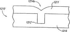
图12A-B示意性地示出根据本发明的一个实施方案从微电子基底1210中除去半导体材料1211的上述方法和装置。在该实施方案的一个方面,微电子基底1210可以包括基底材料1215,基底材料1215有一个其中放置半导体材料1211的凹槽1212。基底材料可以包括磷酸硼硅玻璃(BPSG)或其它基底材料。在一个实施方案中,半导体材料1211可以包括掺杂有磷或硼的多晶硅,在其它实施方案中,半导体材料1211可以包括其它组合物。在任何一个这些实施方案中,半导体材料1211都可以具有正好在凹槽1212上方的凹陷表面1214a。可以用下述方法除去部分半导体材料1211,形成平整的表面1214b(图12b):电解氧化半导体材料1211,然后一般用上述的化学和/或机械力除去半导体材料1211。Figures 12A-B schematically illustrate the above-described method and apparatus for removingsemiconductor material 1211 from amicroelectronic substrate 1210 according to one embodiment of the present invention. In one aspect of this embodiment,microelectronic substrate 1210 can include asubstrate material 1215 having arecess 1212 in whichsemiconductor material 1211 is placed. The substrate material may include borophosphate silicon glass (BPSG) or other substrate materials. In one embodiment, thesemiconductor material 1211 may include polysilicon doped with phosphorous or boron, and in other embodiments, thesemiconductor material 1211 may include other compositions. In any of these embodiments, thesemiconductor material 1211 can have a recessedsurface 1214a just above thegroove 1212 . Portions ofsemiconducting material 1211 may be removed to formplanar surface 1214b (FIG. 12b) by electrolytic oxidation ofsemiconducting material 1211, followed by chemical and/or mechanical removal ofsemiconducting material 1211, typically as described above.

除去掺杂多晶硅的传统技术包括用pH是约10.5至约11.5的浆液平整多晶硅。传统浆液一般包括氢氧化四甲铵(TMAH)和悬浮的二氧化硅磨料颗粒。根据本发明的实施方案,脱除多晶硅和其它半导体材料的方法的优点是不使用磨料元素即可除去材料,用pH小于10.5或大于11.5的电解液可以除去材料。因此,用户可以选择比传统使用的电解液的pH范围更大的电解液(如上所述的那些电解液)。Conventional techniques for removing doped polysilicon include planing the polysilicon with a slurry having a pH of about 10.5 to about 11.5. Traditional slurries typically include tetramethylammonium hydroxide (TMAH) and suspended silica abrasive particles. Advantages of methods of removing polysilicon and other semiconductor materials according to embodiments of the present invention are that material can be removed without the use of abrasive elements, and that material can be removed with an electrolyte having a pH of less than 10.5 or greater than 11.5. Thus, the user can select an electrolyte solution (such as those described above) that has a wider pH range than conventionally used electrolytes.

例如,在一个具体的实施方案中,电解液可以包括稀释的氢氟酸或氢氧化铵和TMAH的组合物。For example, in a specific embodiment, the electrolyte may include diluted hydrofluoric acid or a combination of ammonium hydroxide and TMAH.

用于磷掺杂的多晶硅时,施加于半导体材料1211的电压可以是约25伏rms至约100伏rms。对于硼掺杂的多晶硅,电解液可以包括氢氟酸和TMAH的混合物,施加于半导体材料的电压可以约等于前面讨论磷掺杂的多晶硅时的电压。For phosphorus-doped polysilicon, the voltage applied to thesemiconductor material 1211 may be about 25 volts rms to about 100 volts rms. For boron-doped polysilicon, the electrolyte may include a mixture of hydrofluoric acid and TMAH, and the voltage applied to the semiconductor material may be approximately equal to that previously discussed for phosphorus-doped polysilicon.

本发明的实施方案的方法的另一个优点是为了从微电子基底1210中除去半导体材料1211而选择的电解液与基底材料1215的化学反应性可以很小或没有。因此,对于要将半导体材料1211脱除到低于基底材料1215高度的应用领域,当基底材料1215暴露时,脱除过程自动停止(即,到达终点)。因此,该方法可以省去其它更大的麻烦和/或精度更小的传统终点技术。Another advantage of the methods of embodiments of the present invention is that the electrolyte selected for removal of thesemiconductor material 1211 from themicroelectronic substrate 1210 may have little or no chemical reactivity with thesubstrate material 1215 . Therefore, for applications where thesemiconductor material 1211 is to be removed to a height lower than thebase material 1215, when thebase material 1215 is exposed, the removal process automatically stops (ie, reaches the end point). Thus, this method can save other more cumbersome and/or less accurate traditional endpoint techniques.

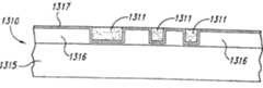
图13A-C示意性地示出应用上述技术和装置从微电子基底1310中除去第一种导电材料1311和第二种导电材料1317的方法。微电子基底1310可以包括具有介电部分1316的基底材料1315(如氧化层),在介电部分1316上形成有凹槽1312或其它部件。第二种导电材料1317放置在凹槽1312中和介电部分1316上(例如以阻挡层的形式),第一种导电材料1311放置在第二种导电材料1317上。在一个实施方案中,第一种导电材料1311可以包括铜,第二种导电材料1317可以包括钽、氮化钽、钨、氮化钨、钛、氮化钛、氮化钛硅和/或氮化钽硅。在其它实施方案中,第一种和第二种导电材料1311、1317可以包括其它组合物。13A-C schematically illustrate a method of removing firstconductive material 1311 and secondconductive material 1317 from amicroelectronic substrate 1310 using the techniques and apparatus described above.Microelectronic substrate 1310 may include a base material 1315 (eg, an oxide layer) having adielectric portion 1316 on which recesses 1312 or other features are formed. The secondconductive material 1317 is placed in thegroove 1312 and on the dielectric portion 1316 (eg, in the form of a barrier layer), and the firstconductive material 1311 is placed on the secondconductive material 1317 . In one embodiment, the firstconductive material 1311 can include copper and the secondconductive material 1317 can include tantalum, tantalum nitride, tungsten, tungsten nitride, titanium, titanium nitride, titanium silicon nitride, and/or nitrogen. tantalum silicon oxide. In other embodiments, the first and secondconductive materials 1311, 1317 may comprise other compositions.

现在参考图13B,用前面参考图9-11时所述的任一装置都可以将第一种导电材料1311脱除到低于第二种导电材料1317的高度。在该实施方案的一个方面,用于脱除第一种导电材料1311的电解液可以包括稀释的H3PO4或有机酸如柠檬酸铵。电解液可以包括浓度类似于上述浓度的氯离子。在该实施方案的一个方面,可以用氯离子浓度控制第一种导电材料1311的脱除速度。例如,用选择浓度的氯离子可以达到最大脱除速度,这取决于电解液的其它组分及第一种导电材料1311的组成。从选择的浓度起始增加或降低氯离子浓度可以降低材料脱除速度。在该实施方案的另一方面,为了减慢材料脱除速度,可以加入醇(如异丙醇或丙酮),该方法可以和控制氯离子浓度方法结合使用,或者取代控制氯离子浓度的方法。Referring now to FIG. 13B, the firstconductive material 1311 may be removed below the level of the secondconductive material 1317 using any of the apparatus previously described with reference to FIGS. 9-11. In one aspect of this embodiment, the electrolyteused to remove the firstconductive material 1311 may include dilutedH3PO4 or an organic acid such as ammonium citrate. The electrolyte may include chloride ions in concentrations similar to those described above. In one aspect of this embodiment, the chloride ion concentration can be used to control the removal rate of the firstconductive material 1311. For example, the maximum removal rate can be achieved with a selected concentration of chloride ions, depending on the other components of the electrolyte and the composition of the firstconductive material 1311. Increasing or decreasing the chloride ion concentration from a selected concentration can decrease the rate of material removal. In another aspect of this embodiment, an alcohol such as isopropanol or acetone may be added in order to slow down the rate of material removal, and this method may be used in conjunction with, or instead of, the method of controlling the chloride ion concentration.

当第一种导电材料1311包括铜时,抛光垫施加在第一种导电材料1311上的下挫力可以在小于1psi至几个psi的压力范围内变化。另外,至少靠近第一种导电材料1311的电极材料可以包括铂或石墨,施加在电极上的电势可以在约1伏至约15伏的范围内变化,这取决于电解液的组成。不管第一种导电材料1311是否包括铜或其它元素、化合物或混合物,其与第一种导电材料1311的化学反应都可以包括刻蚀法、络合法和/或螯合法。When the firstconductive material 1311 includes copper, the downward force exerted by the polishing pad on the firstconductive material 1311 can range from less than 1 psi to several psi of pressure. Additionally, the electrode material at least adjacent to the firstconductive material 1311 may include platinum or graphite, and the potential applied to the electrodes may range from about 1 volt to about 15 volts, depending on the composition of the electrolyte. Regardless of whether the firstconductive material 1311 includes copper or other elements, compounds or mixtures, the chemical reaction with the firstconductive material 1311 may include etching, complexation and/or chelation.

现在参考图13C,用大致类似于上述的方法和装置可以将第二种导电材料1317脱除到低于介电部分1316的高度。在第二种导电材料1317包括钽的该实施方案的一个具体方面,放置在第二种导电材料1317上面的电解液可以包括稀盐酸、NH4Cl和/或稀磷酸或或任何有机或无机酸。在该实施方案的另一方面,电解液可以包括腐蚀抑制剂,用于抑制暴露的第一种导电材料1311受到腐蚀。例如,当第一种导电材料1311包括铜时,腐蚀抑制剂可以包括BTA。在该实施方案的另一方面,靠近第二种导电材料1317的电极可以包括石墨,施加于电极的电压可以约等于施加于第一种导电材料1311的电压。一种替代方案是,施加于第二种导电材料1317的电压可以不同。在一个实施方案中,施加于第二种导电材料1317的下挫力可以等于施加于第一种导电材料1311的下挫力,施加于第二种导电材料1317的下挫力也可以不同于施加于第一种导电材料1311的下挫力。Referring now to FIG. 13C, the secondconductive material 1317 may be removed below the level of thedielectric portion 1316 using methods and apparatus generally similar to those described above. In a specific aspect of this embodiment where the secondconductive material 1317 comprises tantalum, the electrolyte solution placed over the secondconductive material 1317 may comprise dilute hydrochloric acid,NH4Cl and/or dilute phosphoric acid or any organic or inorganic acid . In another aspect of this embodiment, the electrolyte may include a corrosion inhibitor for inhibiting corrosion of the exposed firstconductive material 1311. For example, when the firstconductive material 1311 includes copper, the corrosion inhibitor may include BTA. In another aspect of this embodiment, the electrodes adjacent to the secondconductive material 1317 can comprise graphite, and the voltage applied to the electrodes can be approximately equal to the voltage applied to the firstconductive material 1311. Alternatively, the voltage applied to the secondconductive material 1317 can be different. In one embodiment, the downward force applied to the secondconductive material 1317 may be equal to the downward force applied to the firstconductive material 1311, and the downward force applied to the secondconductive material 1317 may also be different from that applied to the first conductive material. The drop force of theconductive material 1311.

在该实施方案的另一方面,当抛光垫咬合开始时埋藏的介电部分1316时,脱除第二种导电材料1317的过程可以自动停止。因此,本发明的实施方案的方法的优点是:因为不需要具体导向终点的步骤,所以将脱除第二种导电材料1317的过程终止要比传统技术简单。In another aspect of this embodiment, the process of removing the secondconductive material 1317 may automatically stop when the polishing pad engages the initially burieddielectric portion 1316 . Thus, an advantage of the method of embodiments of the present invention is that terminating the process of removing the secondconductive material 1317 is simpler than conventional techniques because no specific end-point steps are required.

上述本发明的实施方案的方法的另一个特点是:在脱除第一种导电材料1311和第二种导电材料1317时,施加于微电子基底1310的下挫力可以小于传统CMP操作(即,不包括电解氧化第一种和第二种导电材料的CMP操作)过程中施加的下挫力。如上所述,该特点的优点是施加下挫力的装置可以具有较长的寿命。另一个优点是比传统下挫力小的下挫力不大可能破坏基底材料1315和/或施加下挫力前形成在基底材料1315中的结构。当基底材料1315具有低介电常数时,例如,其介电常数是约1.5至约3.0时,该特点特别有利。这些材料可以包括多孔二氧化硅。Another feature of the method of the above-described embodiments of the present invention is that when removing the firstconductive material 1311 and the secondconductive material 1317, the downward force applied to themicroelectronic substrate 1310 can be less than that of a conventional CMP operation (i.e., without The downward force applied during the CMP operation including the electrolytic oxidation of the first and second conductive materials). As mentioned above, the advantage of this feature is that the means for applying the down force can have a longer life. Another advantage is that a lower than conventional drop force is less likely to damage thebase material 1315 and/or structures formed in thebase material 1315 prior to the application of the drop force. This feature is particularly advantageous when thebase material 1315 has a low dielectric constant, eg, about 1.5 to about 3.0. These materials can include porous silica.

图14A是前面参考图10时所述的一些组件的线路原理图。该电路图也适用于前面参考图3-13C时所述的任何布置。如图14A所示,电源521通过导线528a和528b分别与第一电极520a和第二电极520b偶联。在能够用两组平行电容器和电阻器示意性表示的布置中,电极520a和520b通过电解质531与微电子基底110偶联。FIG. 14A is a schematic circuit diagram of some of the components previously described with reference to FIG. 10 . This circuit diagram also applies to any of the arrangements described above with reference to Figures 3-13C. As shown in FIG. 14A, thepower source 521 is coupled to thefirst electrode 520a and thesecond electrode 520b throughwires 528a and 528b, respectively.Electrodes 520a and 520b are coupled tomicroelectronic substrate 110 throughelectrolyte 531 in an arrangement that can be schematically represented by two sets of parallel capacitors and resistors.

第三个电容器和电阻器示意性地表示微电子基底110相对于大地或其它电势来说是“漂浮”的。A third capacitor and resistor schematically indicates that themicroelectronic substrate 110 is "floating" with respect to ground or other potential.

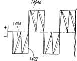
在图14A所示实施方案的一个方面,电源521可以与调幅器522偶联,调幅器522用于调制如图14B所示的由电源521产生的信号。In one aspect of the embodiment shown in Figure 14A, thepower supply 521 can be coupled to anamplitude modulator 522 for modulating the signal generated by thepower supply 521 as shown in Figure 14B.

因此,电源521可以产生高频波1404,调幅器522可以在高频波1404上叠加低频波1402。例如,高频波1404可以包括一系列包含在由低频波1402定义的方波包络线内的正或负电压尖脉冲。高频波1404的每一个尖脉冲都可以具有用于通过介电材料将电荷迁移到电解质的较陡的上升时间坡和更渐进的下降时间坡。下降时间坡可以定义由高频波1404表示的直线或由高频波1404a表示的曲线。在其它实施方案中,高频波1404和低频波1402可以具有其它形状,例如,其取决于介电材料和邻近电极420的电解质的特定性能、基底110的性能和/或从基底110中除去材料的目标速度。Therefore, thepower source 521 can generate ahigh frequency wave 1404 , and theamplitude modulator 522 can superimpose thelow frequency wave 1402 on thehigh frequency wave 1404 . For example,high frequency wave 1404 may include a series of positive or negative voltage spikes contained within a square wave envelope defined bylow frequency wave 1402 . Each spike ofhigh frequency wave 1404 may have a steeper rise time ramp and a more gradual fall time ramp for the migration of charge through the dielectric material to the electrolyte. The falling time slope may define a straight line represented byhigh frequency wave 1404 or a curve represented by high frequency wave 1404a. In other embodiments, thehigh frequency waves 1404 andlow frequency waves 1402 may have other shapes depending, for example, on the particular properties of the dielectric material and electrolyte adjacent to the electrode 420, the properties of thesubstrate 110, and/or the goal of removing material from thesubstrate 110 speed.

该布置的优点是高频信号可以将所需电能从电极520a和520b传送到微电子基底110,而低频叠加信号能够更有效地促进电解质531和微电子基底110的导电层111之间的电化学反应。因此,前面参考图3-13C时所述的任何实施方案都可以包括调幅器和电源。The advantage of this arrangement is that the high frequency signal can transfer the required electrical energy from theelectrodes 520a and 520b to themicroelectronic substrate 110, while the low frequency superimposed signal can more effectively promote the electrochemical reaction between theelectrolyte 531 and theconductive layer 111 of themicroelectronic substrate 110. reaction. Thus, any of the embodiments described above with reference to Figures 3-13C may include an amplitude modulator and a power supply.

从前面的叙述可以知道:尽管为了演示而描述了本发明的具体实施方案,但是不背离本发明的精神和保护范围的情况下可以作出各种改动。例如,上述应用于网式装置(如图9所示的装置)的技术中的一些或全部可以应用于旋转装置(如图11所示的装置),反之亦然。因此,本发明的保护范围由附加的权利要求书限定,不限定于这些具体的实施方案。From the foregoing it will be appreciated that, although specific embodiments of the invention have been described for purposes of illustration, various changes may be made without departing from the spirit and scope of the invention. For example, some or all of the techniques described above applied to a mesh device (such as the device shown in FIG. 9 ) can be applied to a rotating device (such as the device shown in FIG. 11 ), and vice versa. It is therefore intended that the scope of the present invention be defined by the appended claims and not be limited to these specific embodiments.

Claims (77)

CNB02812457XA2001-06-212002-06-20Method and apparatus for electrically, mechanically and/or chemically removing conductive material from microelectronic substratesExpired - Fee RelatedCN100413037C (en)

Applications Claiming Priority (4)

Application NumberPriority DateFiling DateTitle
US09/888,0842001-06-21
US09/887,7672001-06-21
US09/888,084US7112121B2 (en)2000-08-302001-06-21Methods and apparatus for electrical, mechanical and/or chemical removal of conductive material from a microelectronic substrate
US09/888,0022001-06-21

Publications (2)

Publication NumberPublication Date
CN1706035A CN1706035A (en)2005-12-07
CN100413037Ctrue CN100413037C (en)2008-08-20

Family

ID=35578706

Family Applications (1)

Application NumberTitlePriority DateFiling Date
CNB02812457XAExpired - Fee RelatedCN100413037C (en)2001-06-212002-06-20Method and apparatus for electrically, mechanically and/or chemically removing conductive material from microelectronic substrates

Country Status (1)

CountryLink
CN (1)CN100413037C (en)

Families Citing this family (5)

* Cited by examiner, † Cited by third party
Publication numberPriority datePublication dateAssigneeTitle
WO2014089731A1 (en)*2012-12-102014-06-19Acm Research (Shanghai) Inc.Semiconductor wafer polishing method
ES1110830Y (en)*2014-03-282014-08-29Steros Gpa Innovative S L Device for burnishing and polishing metal parts
ES1105980Y (en)*2014-03-282014-07-01Steros Gpa Innovative S L Detachable electromechanical device for burnishing and polishing metal parts
CN112059895B (en)*2020-07-272024-06-18浙江工业大学 ELID grinding method for bearing rollers based on active control of oxide film state
CN117245158B (en)*2023-08-102025-09-16南方科技大学Electrode and electric spark machining equipment

Citations (7)

* Cited by examiner, † Cited by third party
Publication numberPriority datePublication dateAssigneeTitle
US4793895A (en)*1988-01-251988-12-27Ibm CorporationIn situ conductivity monitoring technique for chemical/mechanical planarization endpoint detection
US5807165A (en)*1997-03-261998-09-15International Business Machines CorporationMethod of electrochemical mechanical planarization
US5911619A (en)*1997-03-261999-06-15International Business Machines CorporationApparatus for electrochemical mechanical planarization
US6033953A (en)*1996-12-272000-03-07Texas Instruments IncorporatedMethod for manufacturing dielectric capacitor, dielectric memory device
US6143155A (en)*1998-06-112000-11-07Speedfam Ipec Corp.Method for simultaneous non-contact electrochemical plating and planarizing of semiconductor wafers using a bipiolar electrode assembly
US6171467B1 (en)*1997-11-252001-01-09The John Hopkins UniversityElectrochemical-control of abrasive polishing and machining rates
JP2001077117A (en)*1999-09-072001-03-23Sony CorpManufacture of semiconductor device, and method and device for polishing

Patent Citations (7)

* Cited by examiner, † Cited by third party
Publication numberPriority datePublication dateAssigneeTitle
US4793895A (en)*1988-01-251988-12-27Ibm CorporationIn situ conductivity monitoring technique for chemical/mechanical planarization endpoint detection
US6033953A (en)*1996-12-272000-03-07Texas Instruments IncorporatedMethod for manufacturing dielectric capacitor, dielectric memory device
US5807165A (en)*1997-03-261998-09-15International Business Machines CorporationMethod of electrochemical mechanical planarization
US5911619A (en)*1997-03-261999-06-15International Business Machines CorporationApparatus for electrochemical mechanical planarization
US6171467B1 (en)*1997-11-252001-01-09The John Hopkins UniversityElectrochemical-control of abrasive polishing and machining rates
US6143155A (en)*1998-06-112000-11-07Speedfam Ipec Corp.Method for simultaneous non-contact electrochemical plating and planarizing of semiconductor wafers using a bipiolar electrode assembly
JP2001077117A (en)*1999-09-072001-03-23Sony CorpManufacture of semiconductor device, and method and device for polishing

Also Published As

Publication numberPublication date
CN1706035A (en)2005-12-07

Similar Documents

PublicationPublication DateTitle
US7588677B2 (en)Methods and apparatus for electrical, mechanical and/or chemical removal of conductive material from a microelectronic substrate
JP4446271B2 (en) Method and apparatus for electrically, mechanically and / or chemically removing a conductive material from a microelectronic substrate
US7604729B2 (en)Methods and apparatus for selectively removing conductive material from a microelectronic substrate
CN100503114C (en)Method and apparatus for electromechanically and/or electrochemically-mechanically removing conductive material from a microelectronic substrate
US6893328B2 (en)Conductive polishing pad with anode and cathode
US6379223B1 (en)Method and apparatus for electrochemical-mechanical planarization
US20060199351A1 (en)Method and apparatus for removing adjacent conductive and non-conductive materials of a microelectronic substrate
US20080045009A1 (en)Method and apparatus for simultaneously removing multiple conductive materials from microelectronic substrates
US8603319B2 (en)Methods and systems for removing materials from microfeature workpieces with organic and/or non-aqueous electrolytic media
CN101176988A (en) Electrochemical mechanical milling system and method for detecting milling end point
US20060217040A1 (en)Methods and apparatus for removing conductive material from a microelectronic substrate
JP2005537640A (en) Method and apparatus for chemically, mechanically and / or electrolytically removing material from a microelectronic substrate
CN100413037C (en)Method and apparatus for electrically, mechanically and/or chemically removing conductive material from microelectronic substrates

Legal Events

DateCodeTitleDescription
C06Publication
PB01Publication
C10Entry into substantive examination
SE01Entry into force of request for substantive examination
C14Grant of patent or utility model
GR01Patent grant
C17Cessation of patent right
CF01Termination of patent right due to non-payment of annual fee

Granted publication date:20080820

Termination date:20120620


[8]ページ先頭

©2009-2025 Movatter.jp