CN100412982C - Memory system, buffer device and method for operating the same - Google Patents
Memory system, buffer device and method for operating the sameDownload PDFInfo
- Publication number
- CN100412982C CN100412982CCNB018189857ACN01818985ACN100412982CCN 100412982 CCN100412982 CCN 100412982CCN B018189857 ACNB018189857 ACN B018189857ACN 01818985 ACN01818985 ACN 01818985ACN 100412982 CCN100412982 CCN 100412982C
- Authority
- CN
- China
- Prior art keywords
- clock
- memory device
- buffer
- memory
- address
- Prior art date
- Legal status (The legal status is an assumption and is not a legal conclusion. Google has not performed a legal analysis and makes no representation as to the accuracy of the status listed.)
- Expired - Fee Related
Links
Images


Classifications
- G—PHYSICS
- G06—COMPUTING OR CALCULATING; COUNTING
- G06F—ELECTRIC DIGITAL DATA PROCESSING
- G06F13/00—Interconnection of, or transfer of information or other signals between, memories, input/output devices or central processing units
- G—PHYSICS
- G06—COMPUTING OR CALCULATING; COUNTING
- G06F—ELECTRIC DIGITAL DATA PROCESSING
- G06F13/00—Interconnection of, or transfer of information or other signals between, memories, input/output devices or central processing units
- G06F13/38—Information transfer, e.g. on bus
- G06F13/42—Bus transfer protocol, e.g. handshake; Synchronisation
- G06F13/4204—Bus transfer protocol, e.g. handshake; Synchronisation on a parallel bus
- G06F13/4234—Bus transfer protocol, e.g. handshake; Synchronisation on a parallel bus being a memory bus
- G06F13/4239—Bus transfer protocol, e.g. handshake; Synchronisation on a parallel bus being a memory bus with asynchronous protocol
Landscapes
- Engineering & Computer Science (AREA)
- Theoretical Computer Science (AREA)
- Physics & Mathematics (AREA)
- General Engineering & Computer Science (AREA)
- General Physics & Mathematics (AREA)
- Dram (AREA)
- Communication Control (AREA)
- Synchronisation In Digital Transmission Systems (AREA)
Abstract
Description
Translated fromChinese技术领域technical field
本发明一般涉及利用缓冲结构以隔离存储控制器与存储器件的存储系统,特别涉及在缓冲存储系统中提供信息如数据、状态、指令和地址的可靠传输的系统和方法。该存储器件可以是例如动态随机存取存储器(DRAM)器件。The present invention generally relates to memory systems utilizing buffer structures to isolate memory controllers from memory devices, and more particularly to systems and methods for providing reliable transmission of information such as data, status, instructions and addresses in buffer memory systems. The memory device may be, for example, a dynamic random access memory (DRAM) device.
背景技术Background technique
传统的存储系统包括存储控制器和与之连接的存储器件,如DRAM。在某些系统中,处理器执行存储控制器功能。如这里使用的,术语存储控制器包括这种处理器。存储控制器和存储器件采用存储器接口耦合在一起。存储器接口提供存储控制器和存储器件之间的通信。存储器接口可含有地址总线、指令信号线和数据总线。更高计算机性能和容量的日益增长的需求导致需要更大和更快的存储器。然而,随着工作速度和与芯片组连接的存储模块的数量增加,导致的增加的容性负载可能对存储器的尺寸和速度实质上产生限制。A traditional memory system includes a memory controller and memory devices connected thereto, such as DRAM. In some systems, the processor performs memory controller functions. As used herein, the term memory controller includes such processors. The memory controller and the memory device are coupled together using a memory interface. The memory interface provides communication between the memory controller and the memory devices. A memory interface may contain an address bus, instruction signal lines, and a data bus. The ever-increasing demand for higher computer performance and capacity has resulted in a need for larger and faster memories. However, as operating speeds and the number of memory modules connected to the chipset increase, the resulting increased capacitive loading can substantially limit the size and speed of the memory.
直接连接到存储器总线的存储器件的缺陷在于在存储器件和存储控制器之间没有电压电平隔离以及在存储器总线和存储器件之间没有容性负载隔离。这样,要求每个元件用相同的接口电压和频率工作。因此,存储控制器被制造成利用满足这些参数的特殊存储器件工作。相反,存储器件还只能与具有相同接口电压和工作频率的存储控制器一起使用。因此,与存储控制器一起使用的存储器件被限制到具有与存储控制器相同的接口电压和工作频率的那些器件。A disadvantage of memory devices connected directly to the memory bus is that there is no voltage level isolation between the memory device and the memory controller and no capacitive load isolation between the memory bus and the memory device. Thus, each component is required to work with the same interface voltage and frequency. Therefore, memory controllers are manufactured to work with special memory devices that meet these parameters. In contrast, memory devices can only be used with memory controllers that have the same interface voltage and operating frequency. Therefore, the memory devices used with the memory controller are limited to those devices having the same interface voltage and operating frequency as the memory controller.
而且,随着通过存储器传输的信号频率增加,外部、系统或参考时钟和对于存储控制器或存储器件有效的时间数据之间的固有延迟成了关键性的限制。当存储控制器预计来自存储器件的数据时,对于存储控制器有效的时间数据是很重要的。当存储器件预计来自存储控制器的数据时,对于存储器件有效的时间数据是很重要的。该延迟可以大到足以使下一个时钟周期与数据重叠。即,在一个周期期间该延迟变得很大足以使用于存储控制器或存储器件的数据没准备好,并且这基本上变为“不同步”。Also, as the frequency of signals transmitted through memory increases, the inherent delay between the external, system or reference clock and the time data available to the memory controller or memory device becomes a critical limitation. Time data valid for the memory controller is important when the memory controller anticipates data from the memory device. Time data valid for the memory device is important when the memory device expects data from the memory controller. This delay can be large enough that the next clock cycle overlaps the data. That is, the delay becomes large enough during one cycle that the data for the memory controller or memory device is not ready, and this essentially becomes "out of sync".
在其它存储系统中,已经提出了解决“不同步”难题的解决方案。现有技术设计如线路存储模块中的寄存双重(“寄存DIMM”)系统通过利用独立相位锁定环路芯片访问了这个难题。到寄存DIMM模块的输入时钟进入该独立芯片,该独立芯片的输出用于驱动寄存DIMM系统中的寄存器。然而,寄存DIMM系统中的存储控制器和存储器件被限制成具有相同的接口电压和工作频率。需要特殊设计的存储器件以匹配寄存DIMM系统中的存储控制器的造价,反之亦然,造成了很高的研制费用,并限制了各种现有存储器元件的可互换性。In other storage systems, solutions to the "out of sync" problem have been proposed. Prior art designs such as registered dual ("registered DIMM") systems in line memory modules have addressed this challenge by utilizing independent phase locked loop chips. The input clock to the Registered DIMM module goes into the stand-alone chip, and the output of the stand-alone chip is used to drive the registers in the Registered DIMM system. However, memory controllers and memory devices in a registered DIMM system are constrained to have the same interface voltage and operating frequency. Specially designed memory devices are required to match the cost of memory controllers in registered DIMM systems, and vice versa, resulting in high development costs and limiting the interchangeability of various existing memory components.
发明内容Contents of the invention
因此,针对上述现有技术中的问题,需要提供一种存储系统的系统和方法,其中该存储系统不仅提供可靠的传输以及减少时钟-插入和传播延迟,而且不要求每个元件利用相同的接口电压和频率工作。Therefore, in view of the above-mentioned problems in the prior art, there is a need to provide a system and method of a storage system, wherein the storage system not only provides reliable transmission and reduces clock-insertion and propagation delays, but also does not require each component to utilize the same interface voltage and frequency work.
根据本发明的一个方面,提供一种存储系统,包括:存储数据的至少一个存储器件;向该至少一个存储器件发送信息并从该至少一个存储器件接收数据的存储控制器;互连该至少一个存储器件和该存储控制器的第一缓冲器;和嵌入在第一缓冲器中的时钟电路,其中该时钟电路接收输入时钟和向该至少一个存储器件输出第一输出时钟以控制到该至少一个存储器件的时钟时滞。According to one aspect of the present invention, a storage system is provided, including: at least one storage device for storing data; a storage controller for sending information to the at least one storage device and receiving data from the at least one storage device; interconnecting the at least one A memory device and a first buffer of the memory controller; and a clock circuit embedded in the first buffer, wherein the clock circuit receives an input clock and outputs a first output clock to the at least one memory device to control the at least one The clock skew of the memory device.
根据本发明的另一个方面,提供一种存储系统,包括;存储数据的至少一个存储器件;向该至少一个存储器件发送数据、地址信息和指令信息并从至少一个存储器件接收数据的存储控制器;互连该至少一个存储器件和存储控制器的至少一个数据缓冲器;互连至少一个存储器件和存储控制器的地址和指令缓冲器(addr/cmd缓冲器);和嵌入在该地址和指令缓冲器中的时钟电路,其中该时钟电路接收输入时钟和向至少一个数据缓冲器输出输出时钟以控制到至少一个数据缓冲器的时钟时滞。According to another aspect of the present invention, a storage system is provided, including; at least one storage device storing data; a storage controller for sending data, address information and instruction information to the at least one storage device and receiving data from the at least one storage device ; interconnect the at least one storage device and at least one data buffer of the storage controller; interconnect the address and the instruction buffer (addr/cmd buffer) of the at least one storage device and the storage controller; and embed in the address and the instruction A clock circuit in the buffer, wherein the clock circuit receives an input clock and outputs an output clock to the at least one data buffer to control clock skew to the at least one data buffer.
根据本发明的再一个方面,提供一种互连存储控制器和存储器件的缓冲器件,包括:至少一个数据缓冲器;地址和指令缓冲器,以利于指令信息和地址信息从存储控制器向存储器件的传输;和嵌入在地址和指令缓冲器中的时钟电路,其中时钟电路接收输入时钟和向该至少一个数据缓冲器提供输出时钟以控制到该至少一个数据缓冲器的时钟时滞。According to another aspect of the present invention, there is provided a buffer device for interconnecting a storage controller and a storage device, including: at least one data buffer; and a clock circuit embedded in the address and instruction buffer, wherein the clock circuit receives an input clock and provides an output clock to the at least one data buffer to control clock skew to the at least one data buffer.
根据本发明的再一个方面,提供一种操作存储系统的方法,该存储系统包括存储控制器、存储器件、数据缓冲器和地址/指令缓冲器,该方法包括:从存储控制器经过数据缓冲器向存储器件或从存储器件经过数据缓冲器向存储控制器传输数据;从存储控制器经过地址/指令缓冲器向存储器件传输地址信息和指令信息;在地址/指令缓冲器中接收输入时钟;在输入时钟基础上在地址/指令缓冲器中产生第一输出时钟;从地址/指令缓冲器向数据缓冲器提供第一输出时钟。According to still another aspect of the present invention, there is provided a method of operating a memory system, the memory system comprising a memory controller, a memory device, a data buffer, and an address/instruction buffer, the method comprising: passing from the memory controller through the data buffer Transfer data to the storage device or from the storage device to the storage controller through the data buffer; transfer address information and instruction information from the storage controller to the storage device through the address/instruction buffer; receive the input clock in the address/instruction buffer; A first output clock is generated in the address/instruction buffer based on the input clock; the first output clock is supplied from the address/instruction buffer to the data buffer.
本发明基于采用高速、低成本缓冲器以隔离存储器件与存储控制器。通过采用嵌入在缓冲器中、优选在地址和指令缓冲器中的时钟电路进行数据和指令/地址计时。这种计时方案使数据和指令/地址穿过缓冲器可靠地传输。这种计时方案的优点是精确地控制到数据缓冲器和/或存储器件的时钟时滞;同时又提供了以高频操作存储系统的能力。The present invention is based on the use of high-speed, low-cost buffers to isolate the memory device from the memory controller. Data and instruction/address clocking is done by using clock circuits embedded in the buffers, preferably in the address and instruction buffers. This timing scheme enables reliable transfer of data and instructions/addresses through the buffer. The advantage of this clocking scheme is the precise control of clock skew to the data buffers and/or memory devices; while at the same time providing the ability to operate the memory system at high frequency.
附图说明Description of drawings
图1表示根据本发明实施例的缓冲存储系统的示意图;Fig. 1 represents the schematic diagram of the buffer memory system according to the embodiment of the present invention;
图2表示其中本发明的实施例可执行其功能的缓冲存储系统示意例子;Figure 2 shows a schematic example of a buffer storage system in which an embodiment of the present invention may perform its functions;
图3表示根据本发明实施例的包括嵌入时钟电路的缓冲结构;Figure 3 shows a buffer structure including an embedded clock circuit according to an embodiment of the present invention;
图4表示根据本发明实施例的嵌入时钟电路的相位锁定环路的示意例子;FIG. 4 shows a schematic example of a phase-locked loop embedded in a clock circuit according to an embodiment of the present invention;
图5表示根据本发明实施例的缓冲存储系统;和Figure 5 represents a buffer storage system according to an embodiment of the present invention; and
图6表示根据本发明实施例的用于操作存储系统的程序。FIG. 6 shows a program for operating a storage system according to an embodiment of the present invention.
具体实施方式Detailed ways
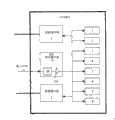
本发明的实施例涉及用于在缓冲存储系统中提供信息如数据、状态、指令和地址的可靠传输的系统和方法。图1表示根据本发明实施例的缓冲存储系统的示意图。缓冲存储系统100包括存储控制器110、缓冲器120、嵌入时钟电路300以及存储器件130-145。缓冲器120是外部缓冲器或寄存器,它们具有减少由存储控制器110检测到的阻抗的功能。存储控制器110耦合到缓冲器120,缓冲器120耦合到存储器件130-145,如DRAM器件。通过将缓冲器120置于存储控制器110和存储器件130-145之间,利于数据和信息在存储控制器110和存储器件130-145之间的传送。还改进了存储系统100的电特性和允许更宽调整。虽然连接线表示为到缓冲器120以及到存储器件130-145的单线,每个示意线实际上可以是多个线。存储控制器110例如可以是芯片组中心处理单元,并且可适于将不同的信息-如数据、状态信息、地址信息、指令信息-经过缓冲器120传输给存储器件130-145。存储控制器110还适于经过缓冲器120从存储器件130-145接收数据。Embodiments of the present invention relate to systems and methods for providing reliable transfer of information, such as data, status, instructions, and addresses, in a cache memory system. FIG. 1 shows a schematic diagram of a buffer storage system according to an embodiment of the present invention.
在本例中,缓冲器120包括多个专用缓冲器或寄存器:用于缓冲数据的数据缓冲器123以及用于缓冲从存储控制器110传输的地址信息和指令信息和/或从存储器件130-145传输的状态信息的地址和指令缓冲器122。在ADDR/CMD缓冲器122内,嵌入时钟电路300。ADDR/CMD缓冲器122接收施加给嵌入时钟电路300的输入时钟或选通脉冲(strobe)。嵌入时钟电路300提供一个输出时钟给数据缓冲器123、124。采用嵌入时钟电路300,以便在缓冲存储系统中提供可靠传输。特别是,数据缓冲器123、124的计时与ADDR/CMD缓冲器122的计时同步。通过将缓冲器120置于存储控制器110和存储器件130-145之间以及将时钟电路300嵌入在ADDR/CMD缓冲器122中的结合,可进一步提高存储系统10电特性,同时提供可靠的传输。In this example, the
图2表示本发明的实施例可在其中执行功能的缓冲存储系统的示意例子。在本例中,存储控制器110位于母板200上。存储器件130-145、170-185位于存储模块150、155上。存储模块150、155通过连接器160、165连接到母板200。存储器件130-145位于第一存储模块150上,而存储器件170-185位于第二存储模块155上。在其它实施例中,存储器件130-145、170-185在存储模块150、155上的构形可以不同,并且存储控制器110可控制比图2中所示的那些存储器件更多或更少的存储器件。Figure 2 shows a schematic example of a cache storage system in which embodiments of the present invention may function. In this example, the
在本例中,缓冲器120和125分别位于存储模块150和155上,产生时钟电路嵌入在其中的缓冲模块以提供在缓冲存储系统中的可靠传输。然而,缓冲器120、125以及缓冲器120、125的独立部件如数据缓冲器123、124和ADDR/CMD缓冲器122不限于图2中所示的设置。就是说,它们不限于设置在存储模块上。数据和指令/地址的缓冲还可以在母板器件200上或在外部(独立)缓冲器上进行。在一个实施例中,采用外部(独立的)缓冲器以允许不同的电压和频率用于存储控制器110和存储器件130-145、170-185。In this example, buffers 120 and 125 are located on
通过将时钟电路嵌入到ADDR/CMD缓冲器122中并时钟电路控制到数据缓冲器123、124的时钟时滞(skew),可在不引入由于传播延迟造成的误差的情况下精确地对缓冲存储系统中的数据缓冲器123、124和ADDR/CMD缓冲器122进行计时。图3表示根据本发明实施例的包括嵌入时钟电路300的缓冲结构。该缓冲结构将存储控制器和存储器件互连。在本例中,该缓冲结构包括两个数据缓冲器123、124以及ADDR/CMD缓冲器122。在其它实施例中,该缓冲结构可包括更多或更少的数据缓冲器和/或ADDR/CMD缓冲器。在其它部件当中,采用数据缓冲器123、124利于数据在存储控制器和存储器件之间的传输。在其它部件当中,采用ADDR/CMD缓冲器122利于指令信息和地址信息从存储控制器传输到存储器件。嵌入在ADDR/CMD缓冲器122中的是嵌入时钟电路300。输入时钟10施加于ADDR/CMD缓冲器122。输入时钟10由存储控制器110或由外部源驱动。由存储控制器110或外部源驱动的时钟例如可以是用于包含缓冲存储系统的计算机的基本时钟或用于存储控制器110的基本时钟。在时钟电路200中,消除了时钟时滞,该时钟时滞通常是在源同步系统中由时钟信号在不同的时间到达数据缓冲器123、124和ADDR/CMD缓冲器引起的。消除时钟时滞之后,从时钟电路300输出输出时钟20。时钟电路300控制输出时钟20以具有与输入时钟10相同的相位。时钟电路300还耦合到时钟驱动器310,而时钟驱动器310驱动输出时钟20到数据缓冲器123、124。这样,数据缓冲器123、124和ADDR/CMD缓冲器122由具有相同相位关系的时钟信号计时(clocking),允许存储器件成功地在一个时钟指令内接收所需的信号。By embedding a clock circuit into the ADDR/
可采用各种方法以实现时钟电路300。例如,第一示意方法利用了延迟锁定环路(DLL)。第二示意方法利用了相位锁定环路(PLL)。第三示意方法利用了延迟链。DLL是本领域公知的。在ADDR/CMD缓冲器122中的DLL基本上接收输入时钟10和在ADDR/CMD缓冲器122中偏移(即时间延迟)该输入时钟10。时间延迟时钟即输出时钟20馈送到数据缓冲器123、124,作为它们的输入时钟。这允许数据缓冲器123、124与ADDR/CMD缓冲器122同步。数据以及指令和地址信息被再定时,并且存储器件接收一个时钟指令中的一切信息。DLL的普通结构可包括如下部件:由D型触发器、形成RS触发器的交叉耦合NAND门、AND门以及固定延迟电路构成的相位检测器;包括系列相同延迟元件的数字延迟线;每个延迟元件具有一级的左/右移位寄存器;内部时钟输入和输出缓冲器。在工作中,DLL在延迟线(串联连接)中引入更多或更少的延迟线元件以控制输出信号的时序。Various methods can be employed to implement the
根据本发明的实施例,在时钟电路300中采用DLL以控制到数据缓冲器123、124的时钟时滞并减少时钟-插入和传播延迟。该DLL具有输入信号和反馈输出信号。DLL在两个信号之间比较该延迟并数字地设置延迟链以使两个信号同步。延迟链有大量的级,并且每个级例如可引入十皮秒延迟。连续检测输出信号和输入信号之间的相位差,并进行调整以保持适当的延迟。在本例中,DLL的输入信号是输入时钟10,而DLL的输出信号是输出时钟20。DLL采用输入时钟10,这提供了对ADDR/CMD缓冲器122的计时,并控制从输入时钟20产生的输出时钟20的相位。DLL由此控制输出时钟20和输入时钟10的相对相位关系。在一种实施方式中,DLL人为地向DLL的输入信号即输入时钟10加入足够的延迟,使DLL的输出信号即输出时钟20的相位在DLL的输入信号后面360度。通过这种方式,输出时钟20与输入时钟10处于反(back)对准状态。输出时钟20被驱动出到数据缓冲器123、124并用做数据缓冲器123、124的输入时钟。结果是,由数据缓冲器123、124检测到的时钟具有与进入ADDR/CMD缓冲器122中的时钟精确相同的相位关系。没有DLL的情况下,在时钟信号经过ADDR/CMD缓冲器122时,时钟-插入和传播延迟可能加到时钟信号中,使输出时钟的相位偏移。According to an embodiment of the present invention, a DLL is employed in the
根据本发明的另一实施例,利用PLL实现时钟电路300,用于进行同步。PLL是在输入PLL的输入信号和PLL的反馈环路中的电压控制振荡器的输出信号之间的相位差的相位灵敏检测基础上的闭环频率控制系统。PLL向时钟电路300提供一种能力以便精确控制到数据缓冲器的时钟时滞和减少时钟插入和传播延迟。图4示出了根据本发明实施例的嵌入时钟电路的相位锁定环路的示意例子。PLL包括相位比较器400、低通滤波器410、放大器420、和电压控制器振荡器(VCO)430。VCO430处于反馈环路中。PLL接收输入信号并提供输出信号。在本例中,输入信号是输入时钟10,输出信号是输出时钟20。相位比较器400比较输入时钟10的相位与VCO430的输出相位。如果两个相位不同,相位比较器400产生相位误差信号,该相位误差信号在被低通滤波器400低通过滤和被放大器420放大之后用于在输入频率方向驱动VCO频率。当PLL被“锁定”时,输出信号的频率和相位与输入信号的频率和相位相同。如果输入信号的相位改变,则输出信号的相位跟随。According to another embodiment of the present invention, the
VCO430例如可以是环形振荡器型或多谐振荡器型。相位比较器例如可以是一组平衡缓冲器和高度平衡的D型触发器。与采用DLL相比,采用PLL的优点在于PLL更精确。不象使用DLL时产生的10或50皮秒的增量延迟,PLL具有更好的精度。然而,在数字系统如存储器中,具有模拟特性的PLL可能在主要数字设计中引入模拟设计复杂性。PLL是比DLL更大和更复杂的电路,但是它给时钟电路300提供更精细的控制。
在另一实施例中,代替在嵌入时钟电路中具有DLL或PLL,采用延迟链按照与DLL或PLL相同的方式引入延迟。延迟链是本领域中公知的。在一种实施方式中,该延迟是补偿延迟。该延迟链包括大量延迟元件,每个延迟元件具有固定时间周期。根据缓冲存储系统的条件,可通过调整电路内延迟元件的数量来调整延迟。连续监控对信号的传播有影响的缓冲存储系统的条件,并且相应地调整延迟。In another embodiment, instead of having a DLL or PLL in the embedded clock circuit, a delay chain is employed to introduce delay in the same way as a DLL or PLL. Delay chains are well known in the art. In one embodiment, the delay is a compensation delay. The delay chain includes a large number of delay elements each having a fixed time period. Depending on the conditions of the buffer storage system, the delay can be adjusted by adjusting the number of delay elements in the circuit. Conditions of the buffer storage system that affect the propagation of the signal are continuously monitored and delays are adjusted accordingly.
图5表示根据本发明另一实施例的缓冲存储器,其中采用ADDR/CMD缓冲器驱动到存储器件的时钟。在本例中,包括数据缓冲器123、124和ADDR/CMD缓冲器122的缓冲结构以及存储器件如DRAM被安装在存储模块150中。存储控制器适于经过缓冲结构向存储器件1-8传输信息如数据、状态信息、地址信息和指令信息。存储控制器爱适于经过缓冲结构从存储器件1-8接收数据。在ADDR/CMD缓冲器122内,在其中嵌入时钟电路300和时钟驱动器310。输入时钟或选通脉冲进入ADDR/CMD缓冲器122并经过嵌入时钟电路300。然后嵌入时钟电路300向数据缓冲器123、124和存储器件1-8输出输出时钟。实现嵌入时钟电路300,以便提供可靠的传输,如使数据缓冲器123、124和存储器件1-8的计时与ADDR/CMD缓冲器122的计时同步。FIG. 5 shows a buffer memory according to another embodiment of the present invention, in which an ADDR/CMD buffer is used to drive a clock to a memory device. In this example, a buffer structure including data buffers 123 , 124 and ADDR/
在本例中,不仅时钟驱动器310从时钟电路300到数据缓冲器123、124驱动输出时钟20,时钟驱动器310还驱动到存储器件1-8的输出时钟20。时钟驱动器310优选由几个输出时钟驱动器构成。实际上,该时钟电路缓冲进入模块的时钟并提供到存储器件1-8的时钟的多次复制,由此提高到存储器件1-8的计时精度。时钟电路300例如可利用PLL、DLL或延迟链来实现。在采用PLL的情况下,向存储器件1-8提供缓冲PLL控制时钟,由此提供计时完整性和避免时钟插入延迟。另一方面,可以提供替换的时钟方案,其中时钟电路300为进入存储器件1-8的时钟和进入数据缓冲器123、124的时钟设置不同的延迟。例如,存储器件1-8经受的时钟可设置为比数据缓冲器123、124经受的时钟晚100皮秒。这给存储器件1-8提供100皮秒的更多的安装时间。In this example, not only does the
图6表示根据本发明实施例的用于操作存储系统的程序。该存储系统包括存储控制器、数据缓冲器、ADDR/CMD缓冲器、嵌入时钟电路、和存储器件。在方框P600中,从存储控制器经过数据缓冲器向存储器件传输数据。在其它实施例中,从存储器件经过数据缓冲器向存储控制器传输数据。在方框P610中,从存储控制器经过ADDR/CMD缓冲器向存储器件传输地址信息和指令信息。在方框P620中,ADDR/CMD缓冲器接收输入时钟。在输入时钟基础上,在方框P630中ADDR/CMD缓冲器产生输出时钟。在方框P640中,ADDR/CMD缓冲器向数据缓冲器提供输出时钟,作为数据缓冲器的输入时钟。在本发明的其它实施例中,上述工艺延伸包括ADDR/CMD缓冲器进一步向存储器件提供输出时钟。FIG. 6 shows a program for operating a storage system according to an embodiment of the present invention. The memory system includes a memory controller, a data buffer, an ADDR/CMD buffer, an embedded clock circuit, and a memory device. In block P600, data is transferred from a memory controller to a memory device via a data buffer. In other embodiments, data is transferred from the memory device to the memory controller through a data buffer. In block P610, address information and command information are transmitted from the memory controller to the memory device through the ADDR/CMD buffer. In block P620, the ADDR/CMD buffer receives an input clock. Based on the input clock, the ADDR/CMD buffer generates an output clock in block P630. In block P640, the ADDR/CMD buffer provides an output clock to the data buffer as an input clock to the data buffer. In other embodiments of the present invention, the above process extension includes the ADDR/CMD buffer further providing an output clock to the storage device.
本发明基于采用高速、低成本缓冲器以隔离存储器件与存储控制器。本发明的上述实施例和方法允许采用嵌入在缓冲器中、优选在地址和指令缓冲器中的时钟电路进行数据和指令/地址计时。这种计时方案使数据和指令/地址穿过缓冲器可靠地传输。这种计时方案的优点是精确地控制到数据缓冲器和/或存储器件的时钟时滞。这又提供了以高频操作存储系统的能力。除了提高计时精度和保持计时完整性之外,通过在地址和指令缓冲器122中嵌入时钟电路,还节省了附加成本和模块空间。满足系统要求的PLL或DLL集成在嵌入时钟电路中。不需要外部PLL或DLL来驱动到存储器件的时钟。The present invention is based on the use of high-speed, low-cost buffers to isolate the memory device from the memory controller. The above-described embodiments and methods of the present invention allow data and instruction/address clocking using clock circuits embedded in buffers, preferably address and instruction buffers. This timing scheme enables reliable transfer of data and instructions/addresses through the buffer. An advantage of this clocking scheme is precise control of clock skew to the data buffers and/or storage devices. This in turn provides the ability to operate the storage system at high frequency. In addition to improving timing accuracy and maintaining timing integrity, by embedding clock circuitry in address and
上述说明涉及本发明的特殊实施例,应该理解在不脱离本发明的精神的情况下可以做很多修改。例如,时钟电路300可放在数据缓冲器中并独立工作。所附权利要求趋于覆盖落入本发明的精神和范围内的这些修改。因此这里公开的实施例只是示意性的而非限制性的,本发明的范围由所附权利要求而不是前述说明表示,因此本发明趋于包含在权利要求书的等效含义和范围内的所有变化。The foregoing description relates to specific embodiments of the invention, and it is to be understood that many modifications may be made without departing from the spirit of the invention. For example, the
Claims (25)
Applications Claiming Priority (2)
| Application Number | Priority Date | Filing Date | Title |
|---|---|---|---|
| US09/664,982 | 2000-09-18 | ||
| US09/664,982US6530006B1 (en) | 2000-09-18 | 2000-09-18 | System and method for providing reliable transmission in a buffered memory system |
Publications (2)
| Publication Number | Publication Date |
|---|---|
| CN1475012A CN1475012A (en) | 2004-02-11 |
| CN100412982Ctrue CN100412982C (en) | 2008-08-20 |
Family
ID=24668229
Family Applications (1)
| Application Number | Title | Priority Date | Filing Date |
|---|---|---|---|
| CNB018189857AExpired - Fee RelatedCN100412982C (en) | 2000-09-18 | 2001-09-14 | Memory system, buffer device and method for operating the same |
Country Status (7)
| Country | Link |
|---|---|
| US (1) | US6530006B1 (en) |
| KR (1) | KR100625128B1 (en) |
| CN (1) | CN100412982C (en) |
| AU (1) | AU2001291006A1 (en) |
| DE (1) | DE10196641T1 (en) |
| TW (1) | TW542957B (en) |
| WO (1) | WO2002023352A2 (en) |
Families Citing this family (43)
| Publication number | Priority date | Publication date | Assignee | Title |
|---|---|---|---|---|
| US6643752B1 (en)* | 1999-12-09 | 2003-11-04 | Rambus Inc. | Transceiver with latency alignment circuitry |
| US7404032B2 (en)* | 2000-01-05 | 2008-07-22 | Rambus Inc. | Configurable width buffered module having switch elements |
| US20050010737A1 (en)* | 2000-01-05 | 2005-01-13 | Fred Ware | Configurable width buffered module having splitter elements |
| US7266634B2 (en)* | 2000-01-05 | 2007-09-04 | Rambus Inc. | Configurable width buffered module having flyby elements |
| US6502161B1 (en)* | 2000-01-05 | 2002-12-31 | Rambus Inc. | Memory system including a point-to-point linked memory subsystem |
| US7356639B2 (en)* | 2000-01-05 | 2008-04-08 | Rambus Inc. | Configurable width buffered module having a bypass circuit |
| US7363422B2 (en) | 2000-01-05 | 2008-04-22 | Rambus Inc. | Configurable width buffered module |
| US7010642B2 (en)* | 2000-01-05 | 2006-03-07 | Rambus Inc. | System featuring a controller device and a memory module that includes an integrated circuit buffer device and a plurality of integrated circuit memory devices |
| US6738880B2 (en)* | 2000-06-12 | 2004-05-18 | Via Technologies, Inc. | Buffer for varying data access speed and system applying the same |
| US6530006B1 (en) | 2000-09-18 | 2003-03-04 | Intel Corporation | System and method for providing reliable transmission in a buffered memory system |
| DE10064593A1 (en)* | 2000-12-22 | 2002-08-29 | Siemens Ag | Method and arrangement for data exchange |
| US6877079B2 (en)* | 2001-03-06 | 2005-04-05 | Samsung Electronics Co., Ltd. | Memory system having point-to-point bus configuration |
| US7177288B2 (en)* | 2001-11-28 | 2007-02-13 | Intel Corporation | Simultaneous transmission and reception of signals in different frequency bands over a bus line |
| US7013359B1 (en)* | 2001-12-21 | 2006-03-14 | Cypress Semiconductor Corporation | High speed memory interface system and method |
| US7389387B2 (en)* | 2001-12-31 | 2008-06-17 | Intel Corporation | Distributed memory module cache writeback |
| US6880044B2 (en)* | 2001-12-31 | 2005-04-12 | Intel Corporation | Distributed memory module cache tag look-up |
| US6845424B2 (en)* | 2002-01-31 | 2005-01-18 | Intel Corporation | Memory pass-band signaling |
| KR100518532B1 (en)* | 2002-04-27 | 2005-10-04 | 삼성전자주식회사 | Method and apparatus for transmitting command signal and address signal selectively |
| JP4159415B2 (en)* | 2002-08-23 | 2008-10-01 | エルピーダメモリ株式会社 | Memory module and memory system |
| DE10309919B4 (en)* | 2003-03-07 | 2008-09-25 | Qimonda Ag | Buffer block and memory modules |
| US7120817B2 (en)* | 2003-05-29 | 2006-10-10 | Intel Corporation | Method of signal distribution based on a standing wave within a closed loop path |
| DE10330811B4 (en)* | 2003-07-08 | 2009-08-13 | Qimonda Ag | Semiconductor memory module |
| US20050050375A1 (en)* | 2003-08-29 | 2005-03-03 | Mark Novak | Memory interface system and method |
| US7216247B2 (en)* | 2004-08-05 | 2007-05-08 | Texas Instruments Incorporated | Methods and systems to reduce data skew in FIFOs |
| US20060129712A1 (en)* | 2004-12-10 | 2006-06-15 | Siva Raghuram | Buffer chip for a multi-rank dual inline memory module (DIMM) |
| CN100405337C (en)* | 2004-12-31 | 2008-07-23 | 技嘉科技股份有限公司 | Data transmission device and method and computer quick starting method thereof |
| US7187599B2 (en)* | 2005-05-25 | 2007-03-06 | Infineon Technologies North America Corp. | Integrated circuit chip having a first delay circuit trimmed via a second delay circuit |
| US7464225B2 (en) | 2005-09-26 | 2008-12-09 | Rambus Inc. | Memory module including a plurality of integrated circuit memory devices and a plurality of buffer devices in a matrix topology |
| US7562271B2 (en) | 2005-09-26 | 2009-07-14 | Rambus Inc. | Memory system topologies including a buffer device and an integrated circuit memory device |
| US11328764B2 (en) | 2005-09-26 | 2022-05-10 | Rambus Inc. | Memory system topologies including a memory die stack |
| US7593279B2 (en)* | 2006-10-11 | 2009-09-22 | Qualcomm Incorporated | Concurrent status register read |
| US8143720B2 (en) | 2007-02-06 | 2012-03-27 | Rambus Inc. | Semiconductor module with micro-buffers |
| US7508723B2 (en)* | 2007-05-24 | 2009-03-24 | Entorian Technologies, Lp | Buffered memory device |
| US9128632B2 (en) | 2009-07-16 | 2015-09-08 | Netlist, Inc. | Memory module with distributed data buffers and method of operation |
| US9201817B2 (en) | 2011-08-03 | 2015-12-01 | Montage Technology (Shanghai) Co., Ltd. | Method for allocating addresses to data buffers in distributed buffer chipset |
| CN102915279B (en)* | 2011-08-03 | 2015-05-13 | 澜起科技(上海)有限公司 | Address assignment method for data registers of distributed cache chipset |
| US9299400B2 (en) | 2012-09-28 | 2016-03-29 | Intel Corporation | Distributed row hammer tracking |
| US9542343B2 (en) | 2012-11-29 | 2017-01-10 | Samsung Electronics Co., Ltd. | Memory modules with reduced rank loading and memory systems including same |
| US10324841B2 (en) | 2013-07-27 | 2019-06-18 | Netlist, Inc. | Memory module with local synchronization |
| US10613995B2 (en) | 2015-03-16 | 2020-04-07 | Rambus Inc. | Training and operations with a double buffered memory topology |
| CN106712762A (en)* | 2015-11-18 | 2017-05-24 | 凌阳科技股份有限公司 | Integrated circuit with a plurality of transistors |
| KR102536639B1 (en)* | 2018-08-14 | 2023-05-26 | 에스케이하이닉스 주식회사 | Buffer circuit control circuit of memory device |
| US20250208788A1 (en)* | 2023-12-20 | 2025-06-26 | Advanced Micro Devices, Inc | Fine-Grained Clocking and Clock Distribution in Low Power Double Data Rate Physical Layer Interface |
Citations (3)
| Publication number | Priority date | Publication date | Assignee | Title |
|---|---|---|---|---|
| US5790839A (en)* | 1996-12-20 | 1998-08-04 | International Business Machines Corporation | System integration of DRAM macros and logic cores in a single chip architecture |
| US5946712A (en)* | 1997-06-04 | 1999-08-31 | Oak Technology, Inc. | Apparatus and method for reading data from synchronous memory |
| US6016282A (en)* | 1998-05-28 | 2000-01-18 | Micron Technology, Inc. | Clock vernier adjustment |
Family Cites Families (12)
| Publication number | Priority date | Publication date | Assignee | Title |
|---|---|---|---|---|
| IL96808A (en) | 1990-04-18 | 1996-03-31 | Rambus Inc | Integrated circuit i/o using a high performance bus interface |
| IN188196B (en) | 1995-05-15 | 2002-08-31 | Silicon Graphics Inc | |
| US6128700A (en)* | 1995-05-17 | 2000-10-03 | Monolithic System Technology, Inc. | System utilizing a DRAM array as a next level cache memory and method for operating same |
| JP3986103B2 (en)* | 1996-08-30 | 2007-10-03 | 富士通株式会社 | Semiconductor integrated circuit |
| US6125157A (en) | 1997-02-06 | 2000-09-26 | Rambus, Inc. | Delay-locked loop circuitry for clock delay adjustment |
| JP3865790B2 (en) | 1997-06-27 | 2007-01-10 | 株式会社ルネサステクノロジ | Memory module |
| US6008821A (en)* | 1997-10-10 | 1999-12-28 | International Business Machines Corporation | Embedded frame buffer system and synchronization method |
| US5964880A (en)* | 1997-12-10 | 1999-10-12 | Intel Corporation | Circuit interface synchronization using slave variable delay loop |
| US6047346A (en) | 1998-02-02 | 2000-04-04 | Rambus Inc. | System for adjusting slew rate on an output of a drive circuit by enabling a plurality of pre-drivers and a plurality of output drivers |
| US6014042A (en) | 1998-02-19 | 2000-01-11 | Rambus Incorporated | Phase detector using switched capacitors |
| US6333959B1 (en)* | 2000-04-25 | 2001-12-25 | Winbond Electronics Corporation | Cross feedback latch-type bi-directional shift register in a delay lock loop circuit |
| US6530006B1 (en) | 2000-09-18 | 2003-03-04 | Intel Corporation | System and method for providing reliable transmission in a buffered memory system |
- 2000
- 2000-09-18USUS09/664,982patent/US6530006B1/ennot_activeExpired - Lifetime
- 2001
- 2001-09-14KRKR1020037003944Apatent/KR100625128B1/ennot_activeExpired - Fee Related
- 2001-09-14CNCNB018189857Apatent/CN100412982C/ennot_activeExpired - Fee Related
- 2001-09-14AUAU2001291006Apatent/AU2001291006A1/ennot_activeAbandoned
- 2001-09-14WOPCT/US2001/028930patent/WO2002023352A2/enactiveApplication Filing
- 2001-09-14DEDE10196641Tpatent/DE10196641T1/ennot_activeWithdrawn
- 2001-09-19TWTW090123026Apatent/TW542957B/ennot_activeIP Right Cessation
Patent Citations (3)
| Publication number | Priority date | Publication date | Assignee | Title |
|---|---|---|---|---|
| US5790839A (en)* | 1996-12-20 | 1998-08-04 | International Business Machines Corporation | System integration of DRAM macros and logic cores in a single chip architecture |
| US5946712A (en)* | 1997-06-04 | 1999-08-31 | Oak Technology, Inc. | Apparatus and method for reading data from synchronous memory |
| US6016282A (en)* | 1998-05-28 | 2000-01-18 | Micron Technology, Inc. | Clock vernier adjustment |
Also Published As
| Publication number | Publication date |
|---|---|
| KR20030033070A (en) | 2003-04-26 |
| CN1475012A (en) | 2004-02-11 |
| DE10196641T1 (en) | 2003-08-28 |
| KR100625128B1 (en) | 2006-09-20 |
| WO2002023352A2 (en) | 2002-03-21 |
| WO2002023352A3 (en) | 2002-08-15 |
| HK1063230A1 (en) | 2004-12-17 |
| AU2001291006A1 (en) | 2002-03-26 |
| TW542957B (en) | 2003-07-21 |
| US6530006B1 (en) | 2003-03-04 |
Similar Documents
| Publication | Publication Date | Title |
|---|---|---|
| CN100412982C (en) | Memory system, buffer device and method for operating the same | |
| CN1139016C (en) | Clock latency compensation circuit for DDR timing | |
| US6791381B2 (en) | Method and apparatus for reducing the lock time of a DLL | |
| US6687322B1 (en) | Dual mode clock alignment and distribution device | |
| KR101014440B1 (en) | Slave RWD-2 compatible coprocessor | |
| US7928770B1 (en) | I/O block for high performance memory interfaces | |
| JP4634803B2 (en) | Data acquisition method and apparatus | |
| US8406080B2 (en) | Data output control circuit of a double data rate (DDR) synchronous semiconductor memory device responsive to a delay locked loop (DLL) clock and method thereof | |
| JPH10336008A (en) | Clock generating circuit and semiconductor device | |
| KR20020066381A (en) | Memory system having stub bus configuration | |
| EP1510930A2 (en) | Memory interface system and method | |
| CN113474746A (en) | Low power memory with on-demand bandwidth boost | |
| CN1666290A (en) | Method and apparatus for delay circuit | |
| US8134391B2 (en) | Semiconductor devices with signal synchronization circuits | |
| KR100560644B1 (en) | Integrated circuit device having a clock synchronizing circuit | |
| KR100486922B1 (en) | Semiconductor storage unit | |
| US9281049B1 (en) | Read clock forwarding for multiple source-synchronous memory interfaces | |
| JP3861650B2 (en) | Interface circuit | |
| JP2003167778A (en) | Control and address clock non-distributed memory system | |
| US7230462B2 (en) | Clock signal synchronizing device, and clock signal synchronizing method | |
| JP2002328744A (en) | Semiconductor integrated circuit device | |
| KR100408397B1 (en) | Memory device having exterior delay control mechanism for adjusting internal clock of data processing and memory module including the same | |
| HK1063230B (en) | Memory system, buffering device and method operating a memory system | |
| JP2004070800A (en) | Memory system and memory module | |
| US7319635B2 (en) | Memory system with registered memory module and control method |
Legal Events
| Date | Code | Title | Description |
|---|---|---|---|
| C06 | Publication | ||
| PB01 | Publication | ||
| C10 | Entry into substantive examination | ||
| SE01 | Entry into force of request for substantive examination | ||
| REG | Reference to a national code | Ref country code:HK Ref legal event code:DE Ref document number:1063230 Country of ref document:HK | |
| C14 | Grant of patent or utility model | ||
| GR01 | Patent grant | ||
| REG | Reference to a national code | Ref country code:HK Ref legal event code:GR Ref document number:1063230 Country of ref document:HK | |
| CF01 | Termination of patent right due to non-payment of annual fee | ||
| CF01 | Termination of patent right due to non-payment of annual fee | Granted publication date:20080820 Termination date:20170914 |