CN100412822C - Memory management device and memory device - Google Patents
Memory management device and memory deviceDownload PDFInfo
- Publication number
- CN100412822C CN100412822CCNB200510099944XACN200510099944ACN100412822CCN 100412822 CCN100412822 CCN 100412822CCN B200510099944X ACNB200510099944X ACN B200510099944XACN 200510099944 ACN200510099944 ACN 200510099944ACN 100412822 CCN100412822 CCN 100412822C
- Authority
- CN
- China
- Prior art keywords
- data
- address
- mentioned
- request
- unit
- Prior art date
- Legal status (The legal status is an assumption and is not a legal conclusion. Google has not performed a legal analysis and makes no representation as to the accuracy of the status listed.)
- Expired - Fee Related
Links
Images


Classifications
- G—PHYSICS
- G11—INFORMATION STORAGE
- G11C—STATIC STORES
- G11C16/00—Erasable programmable read-only memories
- G11C16/02—Erasable programmable read-only memories electrically programmable
- G11C16/06—Auxiliary circuits, e.g. for writing into memory
- G11C16/10—Programming or data input circuits
- G11C16/102—External programming circuits, e.g. EPROM programmers; In-circuit programming or reprogramming; EPROM emulators
- G—PHYSICS
- G11—INFORMATION STORAGE
- G11C—STATIC STORES
- G11C16/00—Erasable programmable read-only memories
- G11C16/02—Erasable programmable read-only memories electrically programmable
- G11C16/06—Auxiliary circuits, e.g. for writing into memory
- G11C16/10—Programming or data input circuits
- G11C16/14—Circuits for erasing electrically, e.g. erase voltage switching circuits
- G11C16/16—Circuits for erasing electrically, e.g. erase voltage switching circuits for erasing blocks, e.g. arrays, words, groups
Landscapes
- Memory System (AREA)
- Information Retrieval, Db Structures And Fs Structures Therefor (AREA)
- Read Only Memory (AREA)
- Techniques For Improving Reliability Of Storages (AREA)
Abstract
Translated fromChineseDescription
Translated fromChinese本申请基于并要求2004年9月13日提出的在前日本专利申请No.2004-265806的优先权,这里通过参考来合并其全部内容。This application is based upon and claims priority from prior Japanese Patent Application No. 2004-265806 filed on September 13, 2004, the entire contents of which are hereby incorporated by reference.
技术领域technical field
本发明涉及具备非易失性存储器的存储器管理装置以及存储器装置。The present invention relates to a memory management device and a memory device including a nonvolatile memory.
背景技术Background technique
以往,在作为非易失性存储器一种的NAND闪速存储器对于已经发生数据写入的块发生重写时,需要把要在该理应重写的块中的被重写的数据以外的数据写入到其它物理块中的处理,因此需要很多的处理时间。In the past, when a NAND flash memory, which is a kind of nonvolatile memory, rewrites a block in which data has already been written, it is necessary to write data other than the rewritten data in the block that should be rewritten. processing into other physical blocks, so a lot of processing time is required.
为了去除这样的原本应该写入的数据以外的写入处理,例如,像在特开2003-280822号公报中公开的那样,有对于一个虚拟块,使多个物理块与其相对应的方式。在该方式中,有根据清除命令,通过进行取消虚拟块与物理块的对应的处理,缩短在数据清除时花费的处理时间的技术。In order to remove such write processing other than data that should be originally written, there is a method of associating a plurality of physical blocks with one virtual block as disclosed in Japanese Unexamined Patent Publication No. 2003-280822, for example. In this method, there is a technique of shortening the processing time required for data erasure by performing a process of canceling the correspondence between the virtual block and the physical block according to the erasure command.
在上述的使用了NAND闪速存储器装置即存储卡中,在该存储卡之一的SD存储卡(登录商标)的推荐文件系统中即FAT(文件分配表)文件系统中,在至1GB的容量中,分组尺寸是16K字节。在存储卡中,由于用分组单位分配读和写文件的尺寸,因此大多情况下主设备向存储卡发行的清除的最小单位相同,指定为16K字节。另外,发行到存储卡的清除命令大都是在该存储卡的格式化时。In the above-mentioned memory card using the NAND flash memory device, in the recommended file system of the SD memory card (registered trademark), which is one of the memory cards, that is, the FAT (File Allocation Table) file system, the capacity is up to 1GB , the packet size is 16K bytes. In the memory card, since the size of the read and write files is allocated in units of packets, the minimum unit of clearing issued by the host device to the memory card is often the same, and 16K bytes is specified. In addition, most of the clear commands issued to the memory card are at the time of formatting the memory card.
主设备根据清除命令,对主引导记录(Master Boot Record)进行读入,把存储卡中的地址增加为16KB的同时,顺序清除16KB范围的数据这样的控制。The master device reads the master boot record (Master Boot Record) according to the clear command, increases the address in the memory card to 16KB, and simultaneously clears the data in the 16KB range sequentially.
原本NAND闪速存储器的物理块尺寸大多是16K字节,该尺寸与前面所示的分组尺寸相同。然而,为了减小NAND闪速存储器的芯片尺寸,NAND闪速存储器的物理块尺寸正在逐渐增大为32K字节、128K字节、256K字节、......。The physical block size of the original NAND flash memory is mostly 16K bytes, which is the same as the packet size shown earlier. However, in order to reduce the chip size of the NAND flash memory, the physical block size of the NAND flash memory is gradually increasing to 32Kbytes, 128Kbytes, 256Kbytes, . . . .
为此,在NAND闪速存储器的物理块尺寸是256K字节而且在分组尺寸是16KB的情况下,在要清除NAND闪速存储器的物理块中的16KB范围的数据时,由于在NAND闪速存储器中不能够进行数据的覆盖,因此在该NAND闪速存储器中,需要准备其它的物理块,对于作为物理块尺寸的256K字节中的16KB清除范围以外的数据进行复制。从而,在进行NAND闪速存储器中的一部分数据清除的情况下,其处理时间没有成为与清除尺寸相称的程度,始终需要一定的处理时间。For this reason, when the physical block size of the NAND flash memory is 256K bytes and the packet size is 16KB, when the data in the 16KB range in the physical block of the NAND flash memory is to be cleared, the NAND flash memory Since data cannot be overwritten in the NAND flash memory, it is necessary to prepare another physical block and copy data outside the clear range of 16KB out of 256K bytes as the physical block size. Therefore, when a part of data in the NAND flash memory is erased, the processing time is not commensurate with the erasing size, and a certain amount of processing time is always required.
发明内容Contents of the invention
本发明提供了一种存储器管理装置,管理构成为具有多个块,能够以其各块为清除单位清除数据的非易失性半导体存储器,所述存储器管理装置的特征在于具备:设定单元,在有对于上述非易失性半导体存储器的数据的清除请求时,在包括上述清除请求的清除对象的数据的块中,设定上述清除对象的数据的地址范围;和控制单元,进行控制以便在有对于上述非易失性半导体存储器的数据的读出请求时,在上述读出请求的读出对象的地址范围包含于由上述设定单元设定的地址范围中的情况下,作为上述读出对象的数据输出初始值数据。The present invention provides a memory management device, which manages a nonvolatile semiconductor memory that has a plurality of blocks and can clear data with each block as a clearing unit. The memory management device is characterized in that it includes: a setting unit, When there is a clear request for the data of the above-mentioned nonvolatile semiconductor memory, in the block including the data of the clear object of the above-mentioned clear request, the address range of the data of the above-mentioned clear object is set; and the control unit controls so that in When there is a read request for data of the nonvolatile semiconductor memory, if the address range of the read target of the read request is included in the address range set by the setting unit, the read Object data output initial value data.
本发明还提供了一种存储器管理装置,管理构成为具有多个块,能够以其各块为清除单位清除数据的非易失性半导体存储器,所述存储器管理装置的特征在于具备:设定单元,在有对于上述非易失性半导体存储器的数据的清除请求时,在包括上述清除请求的清除对象的数据的第1块中,设定上述清除对象的数据的地址范围;和管理单元,使物理地址与逻辑地址相对应进行管理,其中,所述物理地址是与由上述设定单元设定的地址范围相同的地址范围相对应的写入了初始值数据的第2块中的物理地址,以及在上述第1块中,从与由上述设定单元设定的地址范围的终端地址连续的地址到该第1块的终端地址为止的地址范围相对应的物理地址。The present invention also provides a memory management device, which manages a nonvolatile semiconductor memory that has a plurality of blocks and can clear data with each block as a clearing unit. The memory management device is characterized in that it includes: a setting unit , when there is a clear request for the data of the above-mentioned non-volatile semiconductor memory, in the first block including the data of the clear object of the above-mentioned clear request, the address range of the data of the above-mentioned clear object is set; and the management unit makes The physical address is managed in correspondence with the logical address, wherein the physical address is a physical address in the second block in which the initial value data is written corresponding to the same address range as the address range set by the setting unit, And, in the first block, a physical address corresponding to an address range from an address consecutive to the end address of the address range set by the setting means to the end address of the first block.
本发明还提供了一种存储器装置,其特征在于具备:非易失性半导体存储器,构成为具有多个块,能够以其各块为消除单位清除数据;设定单元,在有对于该非易失性半导体存储器的数据的清除请求时,在包括上述清除请求的清除对象的数据的块中,设定上述清除对象的数据的地址范围;和控制单元,进行控制以便在有对于上述非易失性半导体存储器的数据的读出请求时,在依据上述读出请求的读出对象的地址范围包含于由上述设定单元设定的地址范围中的情况下,作为上述读出对象的数据输出初始值数据。The present invention also provides a memory device, which is characterized by comprising: a nonvolatile semiconductor memory configured to have a plurality of blocks capable of erasing data with each block as a unit of erasing; When clearing the data of the volatile semiconductor memory, in the block including the clearing object data of the above-mentioned clearing request, set the address range of the data of the above-mentioned clearing object; When a read request of data of a permanent semiconductor memory is requested, if the address range of the read target according to the read request is included in the address range set by the setting unit, the data output as the read target is initialized value data.
依据本发明一个实施形态的存储器管理装置管理具有多个块,构成为能够以其各个块作为清除单位清除数据的非易失性半导体存储器,具备:在具有对于上述非易失性半导体存储器的数据清除请求时,在包括上述清除请求的清除对象的数据在内的块中,设定上述清除对象的数据的地址范围的设定单元、在具有对于上述非易失性半导体存储器的数据的读出请求时,在依据上述读出请求的读出对象的地址范围包含于由上述设定单元设定了的地址范围中的情况下,进行作为上述读出对象的数据输出初始值数据的控制的控制单元。A memory management device according to an embodiment of the present invention manages a nonvolatile semiconductor memory having a plurality of blocks configured to clear data using each block as a clearing unit, and includes: At the time of a clear request, in a block including the clear target data of the clear request, the setting means for setting the address range of the clear target data has a readout function for the data of the nonvolatile semiconductor memory. When the request is made, when the address range of the read target according to the read request is included in the address range set by the setting unit, the control of outputting the initial value data as the data of the read target is performed. unit.
附图说明Description of drawings
附图与说明书相结合并且建立其一部分,举例说明本发明的最佳实施形态,并且与以上给出的描述以及下面给出的最佳实施形态的详细描述一起,用于解释本发明的原理。The accompanying drawings, which are incorporated in and constitute a part of the specification, illustrate the best mode of the invention and, together with the description given above and the detailed description of the best mode given below, serve to explain the principles of the invention.
图1是表示依据本发明实施形态的存储卡的结构例的框图。FIG. 1 is a block diagram showing a configuration example of a memory card according to an embodiment of the present invention.
图2表示清除写入到依据本发明实施形态的存储卡的闪速存储器上的物理块中的一部分数据的顺序(之一)的转移图。Fig. 2 is a transition diagram showing a sequence (part 1) of clearing a part of data written in a physical block in a flash memory of a memory card according to an embodiment of the present invention.
图3表示在写入到依据本发明实施形态的存储卡中的数据的清除处理中使用的清除区指针的第1例子。Fig. 3 shows a first example of a clear area pointer used in clear processing of data written in the memory card according to the embodiment of the present invention.
图4表示在写入到依据本发明实施形态的存储卡中的数据的清除处理时使用的清除区指针的第2例子。Fig. 4 shows a second example of a clear area pointer used in clear processing of data written in the memory card according to the embodiment of the present invention.
图5表示在写入到依据本发明实施形态的存储卡中的数据的清除处理时使用的清除区指针的第3例子。Fig. 5 shows a third example of a clear area pointer used in clear processing of data written in the memory card according to the embodiment of the present invention.
图6表示在写入到遵从本发明实施形态的存储卡中的数据的清除处理时使用的清除区指针的第4例子。Fig. 6 shows a fourth example of the erase area pointer used in the erasure process of data written in the memory card according to the embodiment of the present invention.
图7表示写入到依据本发明的实施形态的存储卡中的数据的清除顺序的一个例子(之二)的转移图。Fig. 7 is a transition diagram showing an example (Part 2) of the procedure for erasing data written in the memory card according to the embodiment of the present invention.
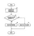
图8是表示写入到依据本发明实施形态的存储卡中的数据的清除顺序的一个例子(之二)的流程图。Fig. 8 is a flowchart showing an example (Part 2) of the procedure for clearing data written in the memory card according to the embodiment of the present invention.
图9是表示写入到依据本发明实施形态的存储卡中的数据的读出顺序的一个例子的流程图。Fig. 9 is a flowchart showing an example of a procedure for reading data written in a memory card according to an embodiment of the present invention.
图10是表示写入到依据本发明实施形态的存储卡中的数据清除顺序的一个例子(之三)的转移图。Fig. 10 is a transition diagram showing an example (Part 3) of the procedure for erasing data written in the memory card according to the embodiment of the present invention.
图11是表示在写入到依据本发明实施形态的存储卡中的数据的清除有无使用清除区指针的选择处理的一个例子的流程图。Fig. 11 is a flow chart showing an example of selection processing of whether or not to use a clear area pointer to clear data written in a memory card according to an embodiment of the present invention.
具体实施方式Detailed ways
以下根据图面说明本发明的一个实施形态。One embodiment of the present invention will be described below with reference to the drawings.
图1是表示依据本发明一个实施形态的存储卡(存储器装置)1的结构例的框图。FIG. 1 is a block diagram showing a configuration example of a memory card (memory device) 1 according to an embodiment of the present invention.
图1所示的存储卡1例如与数码照相机等主设备2连接。The memory card 1 shown in FIG. 1 is connected to a
存储卡1具备闪速存储器控制单元11、主接口单元12、RAM13以及闪速存储器14。闪速存储器14例如是NAND型非易失性存储器。闪速存储器控制单元11经过主接口单元12与主设备2连接。另外,闪速存储器控制单元11与RAM13以及闪速存储器14连接。The memory card 1 includes a flash
来自主设备2向存储卡1所发行的指令通过指令用的信号线,输出到存储卡1内部的主接口单元12。A command issued from the
主接口单元12从来自于主设备2的指令格式抽取指令信息和地址信息。闪速存储器控制单元11进行依据来自主接口单元12的指令信息和地址信息的动作。The
闪速存储器控制单元11进行表示闪速存储器14的物理块与逻辑块的对应关系的与表的管理或者清除有关的管理。The flash
图2是表示清除写入到依据本发明一个实施形态的存储卡1中的闪速存储器14上的物理块中的一部分数据的顺序(之一)的一个例子的转移图。FIG. 2 is a transition diagram showing an example of the procedure (part 1) of clearing a part of data written in the physical block on the
闪速存储器14中的物理块的一块部分的尺寸是128K字节(KB)。闪速存储器14的物理块的一块是256页。可写入到闪速存储器14的物理块的一页中的数据尺寸是512字节。The size of a portion of a physical block in
图2表示在与遍及存储卡1的逻辑块地址“0x40000”地址部分的地址范围相对应的存储区中,写入连续的256KB部分的数据的情况。所谓逻辑块地址,是存储卡1的虚拟存储器上的索引值。逻辑块地址的开始两位“0x”是16进制的识别符。FIG. 2 shows a case where data of consecutive 256 KB portions are written in the storage area corresponding to the address range over the address portion of the logical block address "0x40000" of the memory card 1 . The logical block address is an index value on the virtual memory of the memory card 1 . The first two digits "0x" of the logical block address are hexadecimal identifiers.
闪速存储器14的一块物理块的尺寸是128KB。由此,连续的256KB的数据跨越写入在闪速存储器14上的两个物理块中。The size of one physical block of the
图2所示的“物理块n(n=0、1、2、......)”意味着授予物理块地址“n”的物理块。在图2所示的形态中,上述256KB的数据中,128KB的数据写入到授予物理块地址“3”的物理块中。另外,剩余的128KB尺寸的数据写入到授予物理块地址“5”的物理块中。"Physical block n (n=0, 1, 2, . . . )" shown in FIG. 2 means a physical block assigned a physical block address "n". In the form shown in FIG. 2, among the above-mentioned 256 KB of data, 128 KB of data is written in the physical block assigned the physical block address "3". Also, the remaining data of 128 KB size is written in the physical block assigned the physical block address "5".
RAM13如图1所示,具有逻辑物理地址变换表13a以及清除区指针存储区13b。逻辑物理地址变换表13a在闪速存储器14上的各物理块中,使授予写入着数据的物理块上的物理块地址以及逻辑块地址相对应地进行管理。As shown in FIG. 1, the
例如,所谓在逻辑物理块变换表13a中写入的“0x40000......物理块3”(参照图2),表示逻辑块地址“0x40000”地址与物理块地址“3”相对应。具体地讲,在闪速存储器14中,存储在以逻辑块地址“0x40000”地址作为起始地址,授予“0x20000”地址部分的连续地址范围的逻辑块中所存储的数据意味着存储在授予物理块地址“3”的物理块中。For example, "0x40000...physical block 3" written in the logical-physical block conversion table 13a (see FIG. 2 ) indicates that the logical block address "0x40000" corresponds to the physical block address "3". Specifically, in the
另外,逻辑块地址与物理块地址不存在对应的物理块是未使用状态的物理块。在该未使用状态的物理块中写入初始值数据。当从系统即闪速存储器控制单元11具有对于未使用状态的物理块的读出请求时,读出初始值数据。In addition, a physical block whose logical block address does not correspond to a physical block address is an unused physical block. Initial value data is written in this unused physical block. When there is a readout request for a physical block in an unused state from the system, that is, the flash
该未使用状态的物理块如果依据闪速存储器控制单元11的控制使授予给该物理块的物理块地址与逻辑块地址建立对应关系,则能够使用。The unused physical block can be used if the physical block address assigned to the physical block is associated with the logical block address under the control of the flash
RAM13的清除区指针存储区13b(参照图1)在授予预先规定的物理块地址的物理块的各块中,管理没有写入用户数据即视为写入初始值数据的页的范围。所谓用户数据是初始值数据以外的数据。The clear area
在从主设备2经过主接口单元12,发行对于闪速存储器14上的逻辑块地址“0x40000”地址的服务请求时,闪速存储器控制单元11参照RAM13的逻辑物理地址变换表13a。而且,闪速存储器控制单元11从逻辑物理地址变换表13a检测出在“物理块3”即在授予了与逻辑块地址“0x40000”地址相对应的物理块地址“3”的物理块中写入了数据,读出写入到该物理块中的数据,作为对象数据向主设备2输出。When issuing a service request for the logical block address "0x40000" on the
其次,说明在闪速存储器14中,如果与逻辑块地址“0x4000”地址建立对应关系,则在存储于由逻辑物理地址变换表13a管理的授予物理块地址“3”的物理块中的数据中,当从主设备2发行了清除16384字节(32页)部分数据的指令时,进行依据该指令的处理的顺序的第1例子。这里,假设RAM13没有清除区指针存储区13b。Next, it is explained that in the
这里,在闪速存储器14的物理块中,清除从授予物理块地址“3”的物理块的“页0”到“页31”为止的32页部分的数据。Here, among the physical blocks of the
数据的清除单位由于是物理块的一块部分,因此在授予了物理块地址“3”的物理块的“页32”以后的页中写入的数据也成为清除的对象。Since the erasing unit of data is one block of the physical block, the data written in the pages after "
因此,在闪速存储器14中的授予物理块地址“3”的物理块的各块中,把授予了比“页31”大的页地址的页中写入的数据复制到闪速存储器14中的其它的物理块中。这里,复制对象的物理块是授予了物理块地址“4”的物理块(“物理块4”)。Therefore, in each block of the physical block assigned the physical block address "3" in the
如果向“物理块4”的复制处理结束,则闪速存储器控制单元11把存储在RAM13的逻辑物理地址变换表13a中的“0x40000......物理块地址3””的信息改写为“0x40000......物理块4”。由此,在逻辑物理地址变换表13a中,与逻辑块地址“0x40000”地址相关联的物理块地址从“3”变更为“4”。If the copy processing to "physical block 4" ends, the flash
闪速存储器控制单元11在有从主设备2向闪速存储器14的访问请求时,参照如上述那样改写了信息的逻辑物理地址变换表13a。闪速存储器制单元11视为通过参照该逻辑物理地址变换表13a,把与从逻辑块地址“0x40000”地址到“0x20000”地址部分的地址范围相对应的虚拟存储器上的块中写入的128KB的数据写入到闪速存储器14中的授予了物理块地址“4”的物理块中。When there is an access request from the
根据以上所述,对于闪速存储器14中的具有128KB尺寸的物理块中的256页的区域,清除16KB的数据,即跨越32页部分所写入的数据时,闪速存储控制单元11必须进行读出闪速存储器14的物理块的224页(=256页-32页)部分的数据,把该读出的数据写入到其它物理块中的控制。因此,用于数据清除的处理时间多。According to the above, for the 256-page area in the physical block with a size of 128KB in the
例如,在对于闪速存储器14的物理块写入处理需要的时间是1.2微秒/4页的情况下,224页部分的写入处理所需要的时间是67.2微秒(=224/4*1.2)。一块物理块部分的数据的清除处理所需要的时间是2微秒,物理块的32页部分的数据清除所需要的时间大约是一块物理块部分的数据的清除处理中花费的时间的32倍。For example, when the time required for the physical block write process of the
为了缩短该处理时间,在依据本发明一个实施形态的存储器管理装置中,设置设定清除区指针的功能。In order to shorten the processing time, in the memory management device according to one embodiment of the present invention, a function of setting a clear area pointer is provided.
所谓清除区指针是存储在图1所示的清除区指针存储区13b中的信息。该清除区指针表示在闪速存储器14的物理块的各页中所授予的页地址中,在一部分连续的页上授予的页地址的范围。The so-called clean area pointer is information stored in the clean area
闪速存储器控制单元11把闪速存储器14的物理块的各页中,与用存储在清除区指针存储区13b中的清除区指针表示的地址范围相对应的页视为虚拟清除状态的页。所谓虚拟清除状态,是根据来自主设备2的访问请求,闪速存储器控制单元11在写入到闪速存储器14上的数据中不进行清除对象的数据的物理清除,而在外观上表示清除了的状态。The flash
用清除区指针表示的值作为能够推定闪速存储器14的物理块中的各页中虚拟清除了的部分的值。能够推定虚拟清除的部分的值例如是表示为虚拟清除的区域的最终地点的地址值、来自起始地址的尺寸或者数据成为有效的区域的起始地址值等。The value indicated by the clear area pointer is used as a value capable of estimating the virtually cleared portion of each page in the physical block of the
图3表示清除区指针的第1例子。在该例子中,作为清除区指针是设定开始指针和结束指针的情况。闪速存储器控制单元11根据来自主设备2的清除请求,在闪速存储器14上的写入了清除对象的数据的物理块(物理块A)中,把对写入了清除对象的数据的页群的起始页所授予的页地址指定为开始指针。而且,闪速存储器控制单元11根据来自主设备2的清除请求,把对写入了清除对象的数据的页群的最终页所授予的页地址指定为结束指针。Fig. 3 shows a first example of clear area pointers. In this example, a start pointer and an end pointer are set as clear area pointers. The flash
由此,在闪速存储器14上的写入了清除对象数据的物理块中,与指定为开始指针的页地址到设定为结束指针的页地址的地址范围相对应的页,即,用区域21表示的部分(参照图3)成为虚拟清除部分。Thus, in the physical block in which the erasing object data is written on the
图4表示清除区指针的第2例子。在该例子中,闪速存储器控制单元11与第1例子相同,作为清除区指针设定开始指针和结束指针。但是,在该例子中,在闪速存储器14上的对写入清除对象数据的物理块的起始页所授予的地址成为开始指针,对写入了清除对象数据的物理块的最终页所授予的地址成为结束指针。Fig. 4 shows a second example of clear area pointers. In this example, the flash
这种情况下,闪速存储器控制单元11不需要进行把清除区指针存储在清除区指针存储区13b中的处理,而可以进行应该把该清除对象的物理块整体(区域22)作为未使用状态的处理,即解除用逻辑物理地址变换表13a表示的逻辑块地址与物理块地址(“A”)的对应关系的处理。In this case, the flash
图5表示清除区指针的第3例子。在该例子中,闪速存储器控制单元11把与虚拟清除区的起始相当的页地址定义为是对物理块的起始页所授予的页地址,作为清除区指针,仅设定结束指针。由此,与闪速存储器14中的从对写入了清除对象数据的物理块的起始页所授予的地址到用结束指针指定的地址的地址范围相对应的页,即用区域23表示的部分成为虚拟清除区。Fig. 5 shows a third example of clear area pointers. In this example, the flash
图6表示清除区指针的第4例子。在该例子中,与图3的例子相同,作为清除区指针仅设定结束指针,说明从主设备2发行了跨越闪速存储器14上的多个物理块的清除指令时的处理。Fig. 6 shows a fourth example of clear area pointers. In this example, as in the example of FIG. 3 , only the end pointer is set as the clear area pointer, and the processing when the
这里,表示从主设备2发行了跨越3个物理块(物理块A、B、C)的清除指令的情况。物理块A的最终页由于不是虚拟清除区的终端部分,因此不能够设定虚拟清除区的结束指针。由此,闪速存储器控制单元11对于物理块A的清除对象的区域24,进行图2所示的伴随数据复制的清除处理。Here, a case where the
关于物理块B,由于所有的区域成为清除对象区,因此闪速存储器控制单元11如上所述,通过从逻辑物理地址变换表13a削除物理块B的地址信息以及与该地址信息相对应的逻辑块地址信息,把该物理块的所有区域(区域25)作为未使用状态的块。As for the physical block B, since all the areas are to be erased, the flash
另外,关于物理块C,闪速存储器控制单元11与上述图5所示的例子相同,把对数据清除对象区域的最终部分的页所授予的页地址设定为清除区指针的结束指针。由此,区域26成为虚拟清除区,在写入到物理块C的数据中,不需要移动不是清除对象的数据。As for the physical block C, the flash
例如,在作为清除区指针,闪速存储器控制单元11指定了“页10”的情况下,跨越从物理块C的起始地址到第10页为止的范围的写入数据成为虚拟清除状态。另外,在作为清除区指针,闪速存储器控制单元11指定了“页0”的情况下,意味着物理块C的起始地址以后,即写入到物理块C的各页中的数据全部成为有效数据,虚拟清除的区域没有存在于物理块C中。For example, when the flash
这里,清除区指针存储区13b在闪速存储器14的各物理块中,存储依据来自主设备2的数据清除请求的成为清除对象的数据所存入的物理块中的虚拟清除区的数据,而在RAM13中,在能够确保大量的存储区的情况下,在清除区指针清除区13b中,也可以对于各物理块分别管理虚拟清除区的数据。Here, the clear area
其次,说明清除写入到依据本发明一个实施形态的存储卡1的闪速存储器14上的物理块中的一部分数据的顺序(之二)的一个例子。Next, an example (part 2) of the procedure for clearing a part of data written in the physical block on the
图7是表示写入到依据本发明一个实施形态的存储卡1中的数据的清除顺序(之二)的一个例子的转移图。图8是表示写入到依据本发明一个实施形态的存储卡1中的数据的清除顺序(之二)的一个例子的流程。Fig. 7 is a transition diagram showing an example of a procedure (part 2) of erasing data written in the memory card 1 according to an embodiment of the present invention. Fig. 8 is a flowchart showing an example of the procedure (part 2) of erasing data written in the memory card 1 according to the embodiment of the present invention.
这里,说明与上述的数据清除顺序(之一,参照图2)相同,根据逻辑物理地址变换表13a,在与逻辑块地址“0x40000”地址相对应的授予了物理块地址“3”的物理块地址中进行存储后,则从主设备2发行在所管理的数据中清除16384字节(32页)部分数据的指令时的数据清除顺序。Here, it is the same as the above-mentioned data clearing sequence (one, referring to FIG. 2 ), according to the logical-physical address conversion table 13a, the physical block of the physical block address "3" corresponding to the logical block address "0x40000" address is granted After storing in the address, the data clearing procedure when the
这里,假设RAM13具有清除区指针存储区13b。另外,数据清除请求前的各物理块结构以及由逻辑物理地址变换表13a管理的信息的内容与上述的第1例子相同。Here, it is assumed that the
存储在清除区指针存储区13b中的“开始0x00结束0x00”表示页地址“页0”设定为清除区指针的开始地址以及结束地址,没有设定虚拟清除区。"Start 0x00 End 0x00" stored in the clear area
闪速存储器控制单元11在主设备2进行了数据清除请求时(步骤S1),参照逻辑物理地址变换表13a,检测与在清除请求中指定的地址所授予的逻辑块相对应的物理块的地址(步骤S2)。在图7所示的例子中,闪速存储器控制单元11检测表示逻辑块地址“0x40000”地址与物理块地址“3”相对应的信息。The flash
而且,闪速存储器控制单元11判别与存储了数据清除请求的清除对象数据的区域相对应的地址范围是否已经存储在清除区指针存储区13b中(步骤S3)。Also, the flash
在步骤S3的处理结果判别为「NO 」的情况下,闪速存储器控制单元11为了把存储了数据清除请求中的清除对象数据的区域即与物理块地址“3”相对应的从物理块的0页到第31页的32页部分的区域作为虚拟清除区,把写入到清除区指针存储区13b中的数据改写为“开始0x00结束0x1F”,而且,作为对象块的数据写入“物理块3”(步骤S4)。所谓对象块,是各物理块中写入了虚拟清除对象的数据的页所属的物理块。When the processing result of step S3 is judged to be "NO", the flash
而且,闪速存储器控制单元11判别用在步骤S4的处理中所指定的清除区指针表示的地址范围与块尺寸是否一致,即,用清除区指针表示的开始地址是否是数据清除对象的物理块的起始地址,而且,用清区指针表示的结束地址是否是数据清除对象的物理块的最终地址(步骤S5)。And, the flash
在步骤S5的处理结果判别为「YES 」的情况下,闪速存储控制单元11为了把写入了清除对象的数据的物理块作为未使用状态的块,从逻辑物理地址变换表13a清除给写入了清除对象的数据的物理块所授予的物理块地址,以及与该地址相对应的逻辑块地址的数据(步骤S6)。When the processing result of step S5 is judged to be "YES", the flash
另外,在步骤S5的处理结果判别为「NO 」的情况下,闪速存储器控制单元11把在步骤S4的处理中写入到清除区指针存储区13b中的数据也写入到闪速存储器14中(步骤S7)。通过进行步骤S7的处理,由于即使供给存储卡1的电源断开,也能够保持清除区指针的信息,因此不会解除虚拟清除的状态。In addition, when the processing result of step S5 is judged as "NO", the flash
另外,在向存储卡1供给的电源断开后再次投入的情况下,闪速存储器控制单元11读出在步骤S7的处理中写入到闪速存储器14中的信息,可以把该信息写入到RAM13的清除区指针存储区13b中。In addition, when the power supplied to the memory card 1 is turned off and turned on again, the flash
在步骤S6或者S7的处理以后,闪速存储器控制单元11经过主接口单元12把表示清除处理结束的控制信号输出到主设备2(步骤S8)。After the process of step S6 or S7, the flash
图9是表示写入到依据本发明一个实施形态的存储卡1中的数据的读出顺序的一个例子的流程图。FIG. 9 is a flow chart showing an example of a procedure for reading data written in the memory card 1 according to an embodiment of the present invention.
在依据图8所示的流程图的数据清除处理结束以后,在主设备2进行了数据读出请求的情况下,闪速存储器控制单元11参照逻辑物理地址变换表13a,检测与在数据读出请求中指定的逻辑块地址相对应的物理块地址(步骤A1)。After the data clearing process according to the flow chart shown in FIG. 8 is completed, when the
而且,闪速存储器控制单元11参照清除区指针存储区13b,判别写入了读出对象的数据的页范围是否包含在用清除区指针表示的区域内(步骤A2)。Then, the flash
在步骤A2的处理结果判别为「YES 」的情况下,闪速存储器控制单元11把初始值数据作为读出对象的数据输出到主设备2(步骤A3)。另一方面,在步骤A2的处理结果判别为「NO 」的情况下,闪速存储器控制单元11把该读出对象的数据输出到主设备2(步骤A4)。When the processing result of step A2 is determined as "YES", the flash
这样,通过进行依据清除顺序(之二)的处理,在数据清除时,由于不产生在上述的清除顺序(之一)进行的数据移动,因此能够大幅度地缩短数据清除中所花费的时间。As described above, by performing the processing according to the erasing procedure (two), data movement in the above-mentioned erasing procedure (one) does not occur at the time of data erasing, so the time taken for data erasing can be significantly shortened.
其次,说明清除写入到依据本发明的一个实施形态的存储卡1的闪速存储器14上的物理块中的一部分数据的顺序(之三)的一个例子。Next, an example (part 3) of the procedure for clearing a part of data written in the physical block on the
图10是表示写入到依据本发明一个实施形态的存储卡1中的数据的清除顺序(之三)的一个例子的转移图。Fig. 10 is a transition diagram showing an example of the erasing procedure (Part 3) of data written in the memory card 1 according to an embodiment of the present invention.
这里,说明与上述的清除顺序(之一,参照图2)相同,根据逻辑物理地址变换表13a,当主设备2发行了在授予与逻辑块地址“0x40000”地址相对应的物理块地址“3”的物理块内所存储和所定义的数据中,清除16384字节(32页)部分的数据的指令时的数据清除顺序。另外,数据清除请求前的各物理块的结构以及由逻辑物理地址变换表13a管理的信息的内容与上述的清除顺序(之二,参照图7)相同。Here, the description is the same as the above-mentioned clearing sequence (one, referring to FIG. 2 ). Among the data stored and defined in the physical block, the data clearing sequence when clearing the data of 16384 bytes (32 pages) part of the instruction. In addition, the structure of each physical block before the data erasing request and the content of information managed by the logical-physical address conversion table 13a are the same as the above-mentioned erasing sequence (
闪速存储器控制单元11在主设备2进行了数据清除请求时,参照逻辑物理地址变换表13a,检测与在清除请求中指定的逻辑块地址“0x40000”地址相对应的物理块地址“3”。When the
于是,如果与存储根据数据清除请求的清除对象的数据的区域相对应的地址范围没有存储在清除区指针存储器13b中,则闪速存储器控制单元11为了把存储数据清除请求中的清除对象的数据所存储的区域即与物理块地址“3”相对应的物理块的从第0页到第31页的32页部分的区域作为虚拟清除区,把在RAM13内的逻辑物理地址变换表13a中所存储的“0x40000......物理块“3”的信息改写为“0x40000......物理块3(+物理块4)”。授予了物理块地址“4”的物理块设为写入了初始值数据的状态,即是未使用状态。Then, if the address range corresponding to the area storing the data of the erasing object according to the data erasing request is not stored in the erasing
而且,闪速存储器控制单元11把写入到清除区指针存储区13b中的信息改写为“开始0x00结束0x1F”,作为对象块的数据写入“物理块4”。Furthermore, the flash
由此,与逻辑块地址“0x40000”地址相对应的物理块地址变更为“3”以及“4”的两个,存储在逻辑物理地址变换表13a内的物理块地址“3”以及“4”中,在存储于清除区指针存储区13b内的对象块即授予了物理块地址“4”的物理块的各块中,用存储在清除区指针存储区13b中的清除区指针所表示的页即从“页0”到“页31”的页成为写入了对于清除处理后的来自主设备2的读出请求的读出对象的数据的第1区域。Thus, the physical block address corresponding to the logical block address "0x40000" is changed to two of "3" and "4", and the physical block addresses "3" and "4" stored in the logical-physical address conversion table 13a Among them, in each block of the object block stored in the cleanup area
另外,存储在逻辑物理地址变换表13a内的授予了物理块地址“3”以及“4”的各物理块中,在存储于清除区指针存储区13b内的不是对象块的物理块的各块中,用写入到清除区指针存储区13b中的清除区指针所表示的页范围以外的页范围成为写入了对于清除处理后的来自主设备2的读出请求的读出对象的数据的第2区域。In addition, among the physical blocks assigned physical block addresses "3" and "4" stored in the logical-physical address conversion table 13a, each block of a physical block that is not a target block stored in the clear area
即,该第2区域是存储在逻辑物理地址变换表13a内的物理块地址“3”以及“4”中,在授予了物理块地址“3”的物理块的各页中,从“页0”到“页31”的范围以外的页范围,即从“页32”到“页225”的页。That is, the second area is stored in the physical block addresses "3" and "4" in the logical-physical address conversion table 13a, and in each page of the physical block assigned the physical block address "3", the "page 0 ” to “
于是,在从主设备2进行了数据读出请求的情况下,闪速存储器控制单元11参照逻辑物理地址变换表13a,检测与在数据读出请求中指定的逻辑块地址相对应的物理块地址。Then, when a data read request is made from the
而且,闪速存储器控制单元11参照清除区指针存储区13b,在用清除区指针表示的区域中包括写入了清除对象的数据的页的情况下,闪速存储器控制单元11把初始值数据输出到主设备2。Furthermore, the flash
通过进行这样的处理,由于与上述的清除顺序(之二)相同,不发生在清除顺序(之一)中看到的数据移动,因此能够大幅度地缩短在数据的清除中花费的时间。By performing such processing, similar to the above-mentioned erasing procedure (2), the data migration seen in the erasing procedure (1) does not occur, and thus the time taken for data erasing can be greatly shortened.
在依据本发明一个实施形态的存储卡1中,依照来自主设备2的指示进行数据清除处理时,使用上述的清除区指针,而该清除处理不限于从主设备2指示闪速存储器14的数据格式,即使在从主设备2指示了闪速存储器14的数据复制的情况下也能够进行。在这种情况下,在伴随写处理的清除处理中,使用上述那样的清除区指针的情况下,在该写处理中花费的时间比通常的时间长。In the memory card 1 according to one embodiment of the present invention, when data clearing processing is performed according to an instruction from the
因此,参照图11说明用于防止写处理的时间过长,而且通过使用清除区指针产生缩短数据清除中所花费的时间的优点的顺序。图11是表示写入到依据本发明一个实施形态的存储卡内的数据的清除中,选择是否使用清除区指针的处理的一个例子的流程图。Therefore, the procedure for preventing the writing process from taking too long and producing the advantage of shortening the time spent in data erasing by using the erasure area pointer will be described with reference to FIG. 11 . Fig. 11 is a flowchart showing an example of a process of selecting whether to use a clear area pointer in clearing data written in a memory card according to an embodiment of the present invention.
这里,在从主设备2进行了闪速存储器14的数据格式的指示时,连续发行清除指令,而且,注目于用这些清除指令的变量所表示的清除对象的页地址是连续的情况,根据是否满足该条件,切换在进行数据清除处理时是否使用清除区指针。Here, when the data format of the
从主设备2发行的指令是指示闪速存储器14的数据格式的指令的情况下,以16KB为单位清除数据,由于清除范围边增加16KB边反复进行上述动作,因此清除范围连续。When the command issued from the
具体地讲,存储卡1的闪速存储器控制单元11在识别了从主设备2发行的指令时(步骤B1),判别该指令是否是清除指令(步骤B2)。Specifically, when the flash
在该判别结果判别为「YES 」的情况下,闪速存储器控制单元11把该清除指令的变存储在RAM13中(步骤B3)。When the judgment result is judged as "YES", the flash
而且,闪速存储器控制单元11判别是否已经存储与通过步骤B3的处理存储的变量连续的变量(SB4)。在该判别结果判别为「NO 」的情况下返回到步骤B1的处理。Furthermore, the flash
另一方面,在步骤B4处理的结果判别为「YES 」的情况下,由于意味着逐次发行了变量连续的清除指令,因此闪速存储器控制单元11视为从主设备2发出了用于进行数据格式的指示,进行使用了上述清除区指针的数据清除处理(步骤B5)。On the other hand, when the result of the processing in step B4 is judged to be "YES", since it means that clear commands for consecutive variables have been issued one after another, the flash
另一方面,在上述的步骤B2的处理中判别为「NO 」的情况下,闪速存储器控制单元11判别通过步骤B1的处理识别了的指令是否是写指令(步骤B6)。在该判决结果判别为「YES 」的情况下,闪速存储器控制单元11在RAM13中具有存储的变量的情况下,将其清除(步骤B7)。On the other hand, when it is judged as "NO" in the processing of the above-mentioned step B2, the flash
如果进行这样的处理,则由于只有在从主设备2发行的指令是表示闪速存储器14的数据格式的指令的情况下,进行使用了清除区指针的数据清除处理,因此不会使在写处理中花费的时间成为很长时间,而且能够缩短在数据清除中花费的时间。If such processing is performed, then only when the instruction issued from the
从以往的技术将很容易想到其它的优点和变形。因此,本发明在其广泛的方面并不限于在这里示出和描述的特殊细节和典型的实施例。从而,能够在不脱离一般发明观念的精神或范围的情况下,产生各种变形,该发明观念由附加的权利要求和其等效的要求所定义。Additional advantages and variations will readily occur from the prior art. Therefore, the invention in its broad aspects is not limited to the specific details and typical embodiments shown and described herein. Thus, various modifications can be made without departing from the spirit or scope of the general inventive concept defined by the appended claims and their equivalents.
Claims (9)
Applications Claiming Priority (2)
| Application Number | Priority Date | Filing Date | Title |
|---|---|---|---|
| JP2004265806 | 2004-09-13 | ||
| JP2004265806AJP4192129B2 (en) | 2004-09-13 | 2004-09-13 | Memory management device |
Publications (2)
| Publication Number | Publication Date |
|---|---|
| CN1749974A CN1749974A (en) | 2006-03-22 |
| CN100412822Ctrue CN100412822C (en) | 2008-08-20 |
Family
ID=36035422
Family Applications (1)
| Application Number | Title | Priority Date | Filing Date |
|---|---|---|---|
| CNB200510099944XAExpired - Fee RelatedCN100412822C (en) | 2004-09-13 | 2005-09-13 | Memory management device and memory device |
Country Status (4)
| Country | Link |
|---|---|
| US (3) | US7057942B2 (en) |
| JP (1) | JP4192129B2 (en) |
| CN (1) | CN100412822C (en) |
| TW (1) | TW200622611A (en) |
Families Citing this family (39)
| Publication number | Priority date | Publication date | Assignee | Title |
|---|---|---|---|---|
| US7644239B2 (en) | 2004-05-03 | 2010-01-05 | Microsoft Corporation | Non-volatile memory cache performance improvement |
| JP4192129B2 (en)* | 2004-09-13 | 2008-12-03 | 株式会社東芝 | Memory management device |
| US7490197B2 (en) | 2004-10-21 | 2009-02-10 | Microsoft Corporation | Using external memory devices to improve system performance |
| US7457909B2 (en)* | 2005-01-14 | 2008-11-25 | Angelo Di Sena | Controlling operation of flash memories |
| KR100666174B1 (en)* | 2005-04-27 | 2007-01-09 | 삼성전자주식회사 | 3-level nonvolatile semiconductor memory device and driving method thereof |
| US7634494B2 (en)* | 2005-05-03 | 2009-12-15 | Intel Corporation | Flash memory directory virtualization |
| US20060253643A1 (en)* | 2005-05-04 | 2006-11-09 | Delkin Devices, Inc. | Memory with isolated master boot record |
| JP4751163B2 (en)* | 2005-09-29 | 2011-08-17 | 株式会社東芝 | Memory system |
| US8914557B2 (en) | 2005-12-16 | 2014-12-16 | Microsoft Corporation | Optimizing write and wear performance for a memory |
| US8019938B2 (en) | 2006-12-06 | 2011-09-13 | Fusion-I0, Inc. | Apparatus, system, and method for solid-state storage as cache for high-capacity, non-volatile storage |
| KR100885783B1 (en)* | 2007-01-23 | 2009-02-26 | 주식회사 하이닉스반도체 | Flash memory device and operation method |
| TW200832440A (en) | 2007-01-25 | 2008-08-01 | Genesys Logic Inc | Flash memory translation layer system |
| US7791952B2 (en)* | 2007-01-30 | 2010-09-07 | Micron Technology, Inc. | Memory device architectures and operation |
| KR100823171B1 (en)* | 2007-02-01 | 2008-04-18 | 삼성전자주식회사 | Computer system with partitioned flash translation layer and partitioning method of flash translation layer |
| US7804718B2 (en)* | 2007-03-07 | 2010-09-28 | Mosaid Technologies Incorporated | Partial block erase architecture for flash memory |
| US7719889B2 (en)* | 2007-06-25 | 2010-05-18 | Sandisk Corporation | Methods of programming multilevel cell nonvolatile memory |
| KR101391881B1 (en)* | 2007-10-23 | 2014-05-07 | 삼성전자주식회사 | Multi-bit flash memory device and program and read methods thereof |
| JP2009118212A (en)* | 2007-11-07 | 2009-05-28 | Seiko Epson Corp | Image reading apparatus and image reading method |
| JP5142685B2 (en)* | 2007-11-29 | 2013-02-13 | 株式会社東芝 | Memory system |
| US8631203B2 (en) | 2007-12-10 | 2014-01-14 | Microsoft Corporation | Management of external memory functioning as virtual cache |
| TW200929237A (en)* | 2007-12-21 | 2009-07-01 | Winbond Electronics Corp | Memory architecture and configuration method thereof |
| US20090222613A1 (en)* | 2008-02-29 | 2009-09-03 | Kabushiki Kaisha Toshiba | Information processing apparatus and nonvolatile semiconductor memory drive |
| US20090222614A1 (en)* | 2008-02-29 | 2009-09-03 | Kabushiki Kaisha Toshiba | Information processing apparatus and nonvolatile semiconductor memory drive |
| JP5032371B2 (en)* | 2008-03-01 | 2012-09-26 | 株式会社東芝 | Memory system |
| US8364930B2 (en) | 2008-03-07 | 2013-01-29 | Kabushiki Kaisha Toshiba | Information processing apparatus and storage drive adapted to perform fault analysis by maintenance of tracing information |
| US20090228640A1 (en)* | 2008-03-07 | 2009-09-10 | Kabushiki Kaisha Toshiba | Information processing apparatus and non-volatile semiconductor memory drive |
| TWI370969B (en) | 2008-07-09 | 2012-08-21 | Phison Electronics Corp | Data accessing method, and storage system and controller using the same |
| US8032707B2 (en) | 2008-09-15 | 2011-10-04 | Microsoft Corporation | Managing cache data and metadata |
| US9032151B2 (en) | 2008-09-15 | 2015-05-12 | Microsoft Technology Licensing, Llc | Method and system for ensuring reliability of cache data and metadata subsequent to a reboot |
| US7953774B2 (en) | 2008-09-19 | 2011-05-31 | Microsoft Corporation | Aggregation of write traffic to a data store |
| US20100262979A1 (en)* | 2009-04-08 | 2010-10-14 | Google Inc. | Circular command queues for communication between a host and a data storage device |
| US8433845B2 (en) | 2009-04-08 | 2013-04-30 | Google Inc. | Data storage device which serializes memory device ready/busy signals |
| KR20120132820A (en)* | 2011-05-30 | 2012-12-10 | 삼성전자주식회사 | Storage device, storage system and method of virtualizing a storage device |
| FR3006804A1 (en)* | 2013-06-05 | 2014-12-12 | St Microelectronics Rousset | BLOCK ERASING PROCESS OF A MEMORY OF ERASABLE EEPROM TYPE PER PAGE |
| US10936199B2 (en)* | 2018-07-17 | 2021-03-02 | Silicon Motion, Inc. | Flash controllers, methods, and corresponding storage devices capable of rapidly/fast generating or updating contents of valid page count table |
| US10593412B2 (en)* | 2018-07-19 | 2020-03-17 | Micron Technology, Inc. | Using a status indicator in a memory sub-system to detect an event |
| JP7225991B2 (en)* | 2019-03-22 | 2023-02-21 | 富士フイルムビジネスイノベーション株式会社 | Information processing equipment |
| US12019558B2 (en)* | 2020-12-15 | 2024-06-25 | Intel Corporation | Logical to physical address indirection table in a persistent memory in a solid state drive |
| JP2023019261A (en)* | 2021-07-29 | 2023-02-09 | Necプラットフォームズ株式会社 | MEMORY CONTROL DEVICE, MEMORY CONTROL CIRCUIT, MEMORY CONTROL METHOD AND MEMORY CONTROL PROGRAM |
Citations (4)
| Publication number | Priority date | Publication date | Assignee | Title |
|---|---|---|---|---|
| CN1238846A (en)* | 1996-09-30 | 1999-12-15 | 英特尔公司 | Method for performing continuous over-write of file in nonvolatile memory |
| CN1243317A (en)* | 1998-07-28 | 2000-02-02 | 索尼公司 | Non-volatile memory, recording apparatus and recording method |
| JP2003044351A (en)* | 2001-07-27 | 2003-02-14 | Matsushita Electric Ind Co Ltd | Flash memory device and method of merging data stored therein |
| US20040080998A1 (en)* | 2002-10-28 | 2004-04-29 | Sandisk Corporation | Unusable block management within a non-volatile memory system |
Family Cites Families (9)
| Publication number | Priority date | Publication date | Assignee | Title |
|---|---|---|---|---|
| JP3954698B2 (en) | 1997-08-29 | 2007-08-08 | パナソニック コミュニケーションズ株式会社 | Memory control unit |
| KR100399034B1 (en)* | 2000-05-02 | 2003-09-22 | 한국과학기술원 | The Efficient Management of Memory Cell Array |
| GB0123422D0 (en)* | 2001-09-28 | 2001-11-21 | Memquest Ltd | Improved memory controller |
| US6859856B2 (en)* | 2001-10-23 | 2005-02-22 | Flex P Industries Sdn. Bhd | Method and system for a compact flash memory controller |
| US6798711B2 (en)* | 2002-03-19 | 2004-09-28 | Micron Technology, Inc. | Memory with address management |
| JP3699942B2 (en) | 2002-03-25 | 2005-09-28 | 株式会社東芝 | Memory management method and memory management device |
| JP4188744B2 (en)* | 2003-04-08 | 2008-11-26 | 株式会社ルネサステクノロジ | Memory card |
| JP4157501B2 (en)* | 2004-06-30 | 2008-10-01 | 株式会社東芝 | Storage device |
| JP4192129B2 (en)* | 2004-09-13 | 2008-12-03 | 株式会社東芝 | Memory management device |
- 2004
- 2004-09-13JPJP2004265806Apatent/JP4192129B2/ennot_activeExpired - Fee Related
- 2004-12-28USUS11/022,857patent/US7057942B2/ennot_activeExpired - Lifetime
- 2005
- 2005-08-30TWTW094129671Apatent/TW200622611A/ennot_activeIP Right Cessation
- 2005-09-13CNCNB200510099944XApatent/CN100412822C/ennot_activeExpired - Fee Related
- 2006
- 2006-04-21USUS11/408,021patent/US7227788B2/ennot_activeExpired - Lifetime
- 2007
- 2007-06-04USUS11/757,736patent/US7388792B2/ennot_activeExpired - Lifetime
Patent Citations (4)
| Publication number | Priority date | Publication date | Assignee | Title |
|---|---|---|---|---|
| CN1238846A (en)* | 1996-09-30 | 1999-12-15 | 英特尔公司 | Method for performing continuous over-write of file in nonvolatile memory |
| CN1243317A (en)* | 1998-07-28 | 2000-02-02 | 索尼公司 | Non-volatile memory, recording apparatus and recording method |
| JP2003044351A (en)* | 2001-07-27 | 2003-02-14 | Matsushita Electric Ind Co Ltd | Flash memory device and method of merging data stored therein |
| US20040080998A1 (en)* | 2002-10-28 | 2004-04-29 | Sandisk Corporation | Unusable block management within a non-volatile memory system |
Also Published As
| Publication number | Publication date |
|---|---|
| US7388792B2 (en) | 2008-06-17 |
| US7227788B2 (en) | 2007-06-05 |
| US7057942B2 (en) | 2006-06-06 |
| JP4192129B2 (en) | 2008-12-03 |
| US20060059295A1 (en) | 2006-03-16 |
| TW200622611A (en) | 2006-07-01 |
| TWI310901B (en) | 2009-06-11 |
| US20060187738A1 (en) | 2006-08-24 |
| US20070223286A1 (en) | 2007-09-27 |
| CN1749974A (en) | 2006-03-22 |
| JP2006079543A (en) | 2006-03-23 |
Similar Documents
| Publication | Publication Date | Title |
|---|---|---|
| CN100412822C (en) | Memory management device and memory device | |
| US6625713B2 (en) | Memory controller and method for managing a logical/physical address control table | |
| US7702846B2 (en) | Memory controller, nonvolatile storage device, nonvolatile storage system, and data writing method | |
| CN102332290B (en) | Controller for managing and accessing flash memory modules | |
| KR101409095B1 (en) | Memory device and controlling method of the same | |
| JPWO2005103903A1 (en) | Nonvolatile storage system | |
| JPWO2005029311A1 (en) | Semiconductor memory card, semiconductor memory control device, and semiconductor memory control method | |
| JP2008033788A (en) | Nonvolatile storage device, data storage system, and data storage method | |
| JPWO2005050453A1 (en) | File recording device | |
| JP2010026933A (en) | Memory system and host device | |
| JP5266250B2 (en) | Use of direct data file system with continuous logical address space interface | |
| JP2010515163A (en) | Management of LBA interface in direct data file memory system | |
| CN100428192C (en) | Method of writing data into flash memory | |
| US20100180072A1 (en) | Memory controller, nonvolatile memory device, file system, nonvolatile memory system, data writing method and data writing program | |
| JP2008134685A (en) | Nonvolatile memory system and nonvolatile memory control method | |
| JP4737223B2 (en) | MEMORY CONTROLLER, FLASH MEMORY SYSTEM HAVING MEMORY CONTROLLER, AND FLASH MEMORY CONTROL METHOD | |
| JP2005115562A (en) | Flash rom controller | |
| JP4308780B2 (en) | Semiconductor memory device, memory controller, and data recording method | |
| JP2006277736A (en) | Non-volatile memory device writing method | |
| JP4985108B2 (en) | Data storage device and control method thereof | |
| JP4661086B2 (en) | Nonvolatile memory device and nonvolatile memory erasing and writing method | |
| JP4254930B2 (en) | Memory controller, flash memory system, and flash memory control method | |
| JP2008299513A (en) | Data storage device, and method for controlling the same | |
| JP2004326538A (en) | Information recording/reproducing method |
Legal Events
| Date | Code | Title | Description |
|---|---|---|---|
| C06 | Publication | ||
| PB01 | Publication | ||
| C10 | Entry into substantive examination | ||
| SE01 | Entry into force of request for substantive examination | ||
| C14 | Grant of patent or utility model | ||
| GR01 | Patent grant | ||
| CF01 | Termination of patent right due to non-payment of annual fee | Granted publication date:20080820 Termination date:20170913 | |
| CF01 | Termination of patent right due to non-payment of annual fee |