CN100411198C - light emitting device - Google Patents
light emitting deviceDownload PDFInfo
- Publication number
- CN100411198C CN100411198CCNB2004100053698ACN200410005369ACN100411198CCN 100411198 CCN100411198 CCN 100411198CCN B2004100053698 ACNB2004100053698 ACN B2004100053698ACN 200410005369 ACN200410005369 ACN 200410005369ACN 100411198 CCN100411198 CCN 100411198C
- Authority
- CN
- China
- Prior art keywords
- light
- transparent structure
- light emitting
- emitting element
- emitting device
- Prior art date
- Legal status (The legal status is an assumption and is not a legal conclusion. Google has not performed a legal analysis and makes no representation as to the accuracy of the status listed.)
- Expired - Fee Related
Links
- 239000004065semiconductorSubstances0.000claimsabstractdescription33
- 229920005989resinPolymers0.000claimsabstractdescription27
- 239000011347resinSubstances0.000claimsabstractdescription27
- 238000009826distributionMethods0.000claimsabstractdescription7
- OAICVXFJPJFONN-UHFFFAOYSA-NPhosphorusChemical compound[P]OAICVXFJPJFONN-UHFFFAOYSA-N0.000claimsdescription31
- 239000000758substrateSubstances0.000description14
- 239000012790adhesive layerSubstances0.000description13
- 238000006243chemical reactionMethods0.000description12
- 230000000694effectsEffects0.000description12
- 239000010410layerSubstances0.000description11
- 239000003822epoxy resinSubstances0.000description9
- 238000000605extractionMethods0.000description9
- 229920000647polyepoxidePolymers0.000description9
- 238000004519manufacturing processMethods0.000description7
- 238000000034methodMethods0.000description7
- 229910052594sapphireInorganic materials0.000description7
- 239000010980sapphireSubstances0.000description7
- BQCADISMDOOEFD-UHFFFAOYSA-NSilverChemical compound[Ag]BQCADISMDOOEFD-UHFFFAOYSA-N0.000description6
- 229910052709silverInorganic materials0.000description6
- 239000004332silverSubstances0.000description6
- 229910002601GaNInorganic materials0.000description5
- JMASRVWKEDWRBT-UHFFFAOYSA-NGallium nitrideChemical compound[Ga]#NJMASRVWKEDWRBT-UHFFFAOYSA-N0.000description5
- 239000011247coating layerSubstances0.000description5
- 239000000463materialSubstances0.000description5
- 229910052751metalInorganic materials0.000description5
- 239000002184metalSubstances0.000description5
- 239000000853adhesiveSubstances0.000description4
- 230000001070adhesive effectEffects0.000description4
- 239000004840adhesive resinSubstances0.000description4
- 229920006223adhesive resinPolymers0.000description4
- 229910052782aluminiumInorganic materials0.000description4
- XAGFODPZIPBFFR-UHFFFAOYSA-NaluminiumChemical compound[Al]XAGFODPZIPBFFR-UHFFFAOYSA-N0.000description4
- 239000007787solidSubstances0.000description4
- 239000004593EpoxySubstances0.000description3
- PCHJSUWPFVWCPO-UHFFFAOYSA-NgoldChemical compound[Au]PCHJSUWPFVWCPO-UHFFFAOYSA-N0.000description3
- 229910052737goldInorganic materials0.000description3
- 239000010931goldSubstances0.000description3
- 239000007769metal materialSubstances0.000description3
- 229910000881Cu alloyInorganic materials0.000description2
- 229910052693EuropiumInorganic materials0.000description2
- 210000000078clawAnatomy0.000description2
- 238000000151depositionMethods0.000description2
- 238000009792diffusion processMethods0.000description2
- 238000007599dischargingMethods0.000description2
- 239000000945fillerSubstances0.000description2
- 238000002156mixingMethods0.000description2
- 238000002310reflectometryMethods0.000description2
- PFNQVRZLDWYSCW-UHFFFAOYSA-N(fluoren-9-ylideneamino) n-naphthalen-1-ylcarbamateChemical compoundC12=CC=CC=C2C2=CC=CC=C2C1=NOC(=O)NC1=CC=CC2=CC=CC=C12PFNQVRZLDWYSCW-UHFFFAOYSA-N0.000description1
- 229910018072Al 2 O 3Inorganic materials0.000description1
- 229910001312Amalgam (dentistry)Inorganic materials0.000description1
- 229910004298SiO 2Inorganic materials0.000description1
- XUIMIQQOPSSXEZ-UHFFFAOYSA-NSiliconChemical compound[Si]XUIMIQQOPSSXEZ-UHFFFAOYSA-N0.000description1
- NIXOWILDQLNWCW-UHFFFAOYSA-Nacrylic acid groupChemical groupC(C=C)(=O)ONIXOWILDQLNWCW-UHFFFAOYSA-N0.000description1
- AUCDRFABNLOFRE-UHFFFAOYSA-Nalumane;indiumChemical compound[AlH3].[In]AUCDRFABNLOFRE-UHFFFAOYSA-N0.000description1
- 239000005354aluminosilicate glassSubstances0.000description1
- RNQKDQAVIXDKAG-UHFFFAOYSA-Naluminum galliumChemical compound[Al].[Ga]RNQKDQAVIXDKAG-UHFFFAOYSA-N0.000description1
- 229910052788bariumInorganic materials0.000description1
- 230000005540biological transmissionEffects0.000description1
- 230000015572biosynthetic processEffects0.000description1
- 239000005388borosilicate glassSubstances0.000description1
- 229910052791calciumInorganic materials0.000description1
- 239000000919ceramicSubstances0.000description1
- 229910019990cerium-doped yttrium aluminum garnetInorganic materials0.000description1
- 239000011248coating agentSubstances0.000description1
- 238000000576coating methodMethods0.000description1
- 239000003086colorantSubstances0.000description1
- 230000000295complement effectEffects0.000description1
- 150000001875compoundsChemical class0.000description1
- 238000010276constructionMethods0.000description1
- 238000005520cutting processMethods0.000description1
- 230000008021depositionEffects0.000description1
- 230000005284excitationEffects0.000description1
- 239000002223garnetSubstances0.000description1
- 238000010438heat treatmentMethods0.000description1
- 238000007373indentationMethods0.000description1
- 229910052738indiumInorganic materials0.000description1
- APFVFJFRJDLVQX-UHFFFAOYSA-Nindium atomChemical compound[In]APFVFJFRJDLVQX-UHFFFAOYSA-N0.000description1
- 230000007774longtermEffects0.000description1
- 229910052749magnesiumInorganic materials0.000description1
- 238000012986modificationMethods0.000description1
- 230000004048modificationEffects0.000description1
- 229910003465moissaniteInorganic materials0.000description1
- 238000000465mouldingMethods0.000description1
- 229920001296polysiloxanePolymers0.000description1
- SBIBMFFZSBJNJF-UHFFFAOYSA-Nselenium;zincChemical group[Se]=[Zn]SBIBMFFZSBJNJF-UHFFFAOYSA-N0.000description1
- 229910052710siliconInorganic materials0.000description1
- 239000010703siliconSubstances0.000description1
- 229910010271silicon carbideInorganic materials0.000description1
- 229920002050silicone resinPolymers0.000description1
- 229910052712strontiumInorganic materials0.000description1
- 229910052720vanadiumInorganic materials0.000description1
Images


Classifications
- B—PERFORMING OPERATIONS; TRANSPORTING
- B23—MACHINE TOOLS; METAL-WORKING NOT OTHERWISE PROVIDED FOR
- B23C—MILLING
- B23C3/00—Milling particular work; Special milling operations; Machines therefor
- B23C3/002—Milling elongated workpieces
- H—ELECTRICITY
- H10—SEMICONDUCTOR DEVICES; ELECTRIC SOLID-STATE DEVICES NOT OTHERWISE PROVIDED FOR
- H10H—INORGANIC LIGHT-EMITTING SEMICONDUCTOR DEVICES HAVING POTENTIAL BARRIERS
- H10H20/00—Individual inorganic light-emitting semiconductor devices having potential barriers, e.g. light-emitting diodes [LED]
- H10H20/80—Constructional details
- H10H20/85—Packages
- H10H20/855—Optical field-shaping means, e.g. lenses
- B—PERFORMING OPERATIONS; TRANSPORTING
- B23—MACHINE TOOLS; METAL-WORKING NOT OTHERWISE PROVIDED FOR
- B23C—MILLING
- B23C5/00—Milling-cutters
- B23C5/02—Milling-cutters characterised by the shape of the cutter
- B23C5/10—Shank-type cutters, i.e. with an integral shaft
- H—ELECTRICITY
- H10—SEMICONDUCTOR DEVICES; ELECTRIC SOLID-STATE DEVICES NOT OTHERWISE PROVIDED FOR
- H10H—INORGANIC LIGHT-EMITTING SEMICONDUCTOR DEVICES HAVING POTENTIAL BARRIERS
- H10H20/00—Individual inorganic light-emitting semiconductor devices having potential barriers, e.g. light-emitting diodes [LED]
- H10H20/80—Constructional details
- H10H20/81—Bodies
- H10H20/819—Bodies characterised by their shape, e.g. curved or truncated substrates
- H—ELECTRICITY
- H10—SEMICONDUCTOR DEVICES; ELECTRIC SOLID-STATE DEVICES NOT OTHERWISE PROVIDED FOR
- H10H—INORGANIC LIGHT-EMITTING SEMICONDUCTOR DEVICES HAVING POTENTIAL BARRIERS
- H10H20/00—Individual inorganic light-emitting semiconductor devices having potential barriers, e.g. light-emitting diodes [LED]
- H10H20/80—Constructional details
- H10H20/85—Packages
- H10H20/851—Wavelength conversion means
- H10H20/8511—Wavelength conversion means characterised by their material, e.g. binder
- H10H20/8512—Wavelength conversion materials
- H10H20/8513—Wavelength conversion materials having two or more wavelength conversion materials
- B—PERFORMING OPERATIONS; TRANSPORTING
- B23—MACHINE TOOLS; METAL-WORKING NOT OTHERWISE PROVIDED FOR
- B23C—MILLING
- B23C2220/00—Details of milling processes
- B23C2220/24—Production of elliptical holes
- H—ELECTRICITY
- H01—ELECTRIC ELEMENTS
- H01L—SEMICONDUCTOR DEVICES NOT COVERED BY CLASS H10
- H01L2224/00—Indexing scheme for arrangements for connecting or disconnecting semiconductor or solid-state bodies and methods related thereto as covered by H01L24/00
- H01L2224/01—Means for bonding being attached to, or being formed on, the surface to be connected, e.g. chip-to-package, die-attach, "first-level" interconnects; Manufacturing methods related thereto
- H01L2224/02—Bonding areas; Manufacturing methods related thereto
- H01L2224/04—Structure, shape, material or disposition of the bonding areas prior to the connecting process
- H01L2224/05—Structure, shape, material or disposition of the bonding areas prior to the connecting process of an individual bonding area
- H01L2224/05001—Internal layers
- H01L2224/0502—Disposition
- H01L2224/05023—Disposition the whole internal layer protruding from the surface
- H—ELECTRICITY
- H01—ELECTRIC ELEMENTS
- H01L—SEMICONDUCTOR DEVICES NOT COVERED BY CLASS H10
- H01L2224/00—Indexing scheme for arrangements for connecting or disconnecting semiconductor or solid-state bodies and methods related thereto as covered by H01L24/00
- H01L2224/01—Means for bonding being attached to, or being formed on, the surface to be connected, e.g. chip-to-package, die-attach, "first-level" interconnects; Manufacturing methods related thereto
- H01L2224/02—Bonding areas; Manufacturing methods related thereto
- H01L2224/04—Structure, shape, material or disposition of the bonding areas prior to the connecting process
- H01L2224/05—Structure, shape, material or disposition of the bonding areas prior to the connecting process of an individual bonding area
- H01L2224/0554—External layer
- H01L2224/0556—Disposition
- H01L2224/05568—Disposition the whole external layer protruding from the surface
- H—ELECTRICITY
- H01—ELECTRIC ELEMENTS
- H01L—SEMICONDUCTOR DEVICES NOT COVERED BY CLASS H10
- H01L2224/00—Indexing scheme for arrangements for connecting or disconnecting semiconductor or solid-state bodies and methods related thereto as covered by H01L24/00
- H01L2224/01—Means for bonding being attached to, or being formed on, the surface to be connected, e.g. chip-to-package, die-attach, "first-level" interconnects; Manufacturing methods related thereto
- H01L2224/02—Bonding areas; Manufacturing methods related thereto
- H01L2224/04—Structure, shape, material or disposition of the bonding areas prior to the connecting process
- H01L2224/06—Structure, shape, material or disposition of the bonding areas prior to the connecting process of a plurality of bonding areas
- H01L2224/061—Disposition
- H01L2224/06102—Disposition the bonding areas being at different heights
- H—ELECTRICITY
- H01—ELECTRIC ELEMENTS
- H01L—SEMICONDUCTOR DEVICES NOT COVERED BY CLASS H10
- H01L2224/00—Indexing scheme for arrangements for connecting or disconnecting semiconductor or solid-state bodies and methods related thereto as covered by H01L24/00
- H01L2224/01—Means for bonding being attached to, or being formed on, the surface to be connected, e.g. chip-to-package, die-attach, "first-level" interconnects; Manufacturing methods related thereto
- H01L2224/10—Bump connectors; Manufacturing methods related thereto
- H01L2224/12—Structure, shape, material or disposition of the bump connectors prior to the connecting process
- H01L2224/13—Structure, shape, material or disposition of the bump connectors prior to the connecting process of an individual bump connector
- H—ELECTRICITY
- H01—ELECTRIC ELEMENTS
- H01L—SEMICONDUCTOR DEVICES NOT COVERED BY CLASS H10
- H01L2224/00—Indexing scheme for arrangements for connecting or disconnecting semiconductor or solid-state bodies and methods related thereto as covered by H01L24/00
- H01L2224/01—Means for bonding being attached to, or being formed on, the surface to be connected, e.g. chip-to-package, die-attach, "first-level" interconnects; Manufacturing methods related thereto
- H01L2224/10—Bump connectors; Manufacturing methods related thereto
- H01L2224/15—Structure, shape, material or disposition of the bump connectors after the connecting process
- H01L2224/17—Structure, shape, material or disposition of the bump connectors after the connecting process of a plurality of bump connectors
- H01L2224/1701—Structure
- H01L2224/1703—Bump connectors having different sizes, e.g. different diameters, heights or widths
- H—ELECTRICITY
- H01—ELECTRIC ELEMENTS
- H01L—SEMICONDUCTOR DEVICES NOT COVERED BY CLASS H10
- H01L2224/00—Indexing scheme for arrangements for connecting or disconnecting semiconductor or solid-state bodies and methods related thereto as covered by H01L24/00
- H01L2224/01—Means for bonding being attached to, or being formed on, the surface to be connected, e.g. chip-to-package, die-attach, "first-level" interconnects; Manufacturing methods related thereto
- H01L2224/42—Wire connectors; Manufacturing methods related thereto
- H01L2224/47—Structure, shape, material or disposition of the wire connectors after the connecting process
- H01L2224/48—Structure, shape, material or disposition of the wire connectors after the connecting process of an individual wire connector
- H01L2224/4805—Shape
- H01L2224/4809—Loop shape
- H01L2224/48091—Arched
- H—ELECTRICITY
- H01—ELECTRIC ELEMENTS
- H01L—SEMICONDUCTOR DEVICES NOT COVERED BY CLASS H10
- H01L2224/00—Indexing scheme for arrangements for connecting or disconnecting semiconductor or solid-state bodies and methods related thereto as covered by H01L24/00
- H01L2224/01—Means for bonding being attached to, or being formed on, the surface to be connected, e.g. chip-to-package, die-attach, "first-level" interconnects; Manufacturing methods related thereto
- H01L2224/42—Wire connectors; Manufacturing methods related thereto
- H01L2224/47—Structure, shape, material or disposition of the wire connectors after the connecting process
- H01L2224/48—Structure, shape, material or disposition of the wire connectors after the connecting process of an individual wire connector
- H01L2224/481—Disposition
- H01L2224/48151—Connecting between a semiconductor or solid-state body and an item not being a semiconductor or solid-state body, e.g. chip-to-substrate, chip-to-passive
- H01L2224/48221—Connecting between a semiconductor or solid-state body and an item not being a semiconductor or solid-state body, e.g. chip-to-substrate, chip-to-passive the body and the item being stacked
- H01L2224/48245—Connecting between a semiconductor or solid-state body and an item not being a semiconductor or solid-state body, e.g. chip-to-substrate, chip-to-passive the body and the item being stacked the item being metallic
- H01L2224/48247—Connecting between a semiconductor or solid-state body and an item not being a semiconductor or solid-state body, e.g. chip-to-substrate, chip-to-passive the body and the item being stacked the item being metallic connecting the wire to a bond pad of the item
- H—ELECTRICITY
- H01—ELECTRIC ELEMENTS
- H01L—SEMICONDUCTOR DEVICES NOT COVERED BY CLASS H10
- H01L2224/00—Indexing scheme for arrangements for connecting or disconnecting semiconductor or solid-state bodies and methods related thereto as covered by H01L24/00
- H01L2224/01—Means for bonding being attached to, or being formed on, the surface to be connected, e.g. chip-to-package, die-attach, "first-level" interconnects; Manufacturing methods related thereto
- H01L2224/42—Wire connectors; Manufacturing methods related thereto
- H01L2224/47—Structure, shape, material or disposition of the wire connectors after the connecting process
- H01L2224/49—Structure, shape, material or disposition of the wire connectors after the connecting process of a plurality of wire connectors
- H01L2224/491—Disposition
- H01L2224/49105—Connecting at different heights
- H01L2224/49107—Connecting at different heights on the semiconductor or solid-state body
- H—ELECTRICITY
- H01—ELECTRIC ELEMENTS
- H01L—SEMICONDUCTOR DEVICES NOT COVERED BY CLASS H10
- H01L2224/00—Indexing scheme for arrangements for connecting or disconnecting semiconductor or solid-state bodies and methods related thereto as covered by H01L24/00
- H01L2224/73—Means for bonding being of different types provided for in two or more of groups H01L2224/10, H01L2224/18, H01L2224/26, H01L2224/34, H01L2224/42, H01L2224/50, H01L2224/63, H01L2224/71
- H01L2224/732—Location after the connecting process
- H01L2224/73251—Location after the connecting process on different surfaces
- H01L2224/73265—Layer and wire connectors
- H—ELECTRICITY
- H01—ELECTRIC ELEMENTS
- H01L—SEMICONDUCTOR DEVICES NOT COVERED BY CLASS H10
- H01L2224/00—Indexing scheme for arrangements for connecting or disconnecting semiconductor or solid-state bodies and methods related thereto as covered by H01L24/00
- H01L2224/80—Methods for connecting semiconductor or other solid state bodies using means for bonding being attached to, or being formed on, the surface to be connected
- H01L2224/85—Methods for connecting semiconductor or other solid state bodies using means for bonding being attached to, or being formed on, the surface to be connected using a wire connector
- H01L2224/85909—Post-treatment of the connector or wire bonding area
- H01L2224/8592—Applying permanent coating, e.g. protective coating
- H—ELECTRICITY
- H01—ELECTRIC ELEMENTS
- H01L—SEMICONDUCTOR DEVICES NOT COVERED BY CLASS H10
- H01L24/00—Arrangements for connecting or disconnecting semiconductor or solid-state bodies; Methods or apparatus related thereto
- H01L24/01—Means for bonding being attached to, or being formed on, the surface to be connected, e.g. chip-to-package, die-attach, "first-level" interconnects; Manufacturing methods related thereto
- H01L24/02—Bonding areas ; Manufacturing methods related thereto
- H01L24/04—Structure, shape, material or disposition of the bonding areas prior to the connecting process
- H01L24/05—Structure, shape, material or disposition of the bonding areas prior to the connecting process of an individual bonding area
- H—ELECTRICITY
- H01—ELECTRIC ELEMENTS
- H01L—SEMICONDUCTOR DEVICES NOT COVERED BY CLASS H10
- H01L2924/00—Indexing scheme for arrangements or methods for connecting or disconnecting semiconductor or solid-state bodies as covered by H01L24/00
- H01L2924/0001—Technical content checked by a classifier
- H01L2924/00014—Technical content checked by a classifier the subject-matter covered by the group, the symbol of which is combined with the symbol of this group, being disclosed without further technical details
- H—ELECTRICITY
- H01—ELECTRIC ELEMENTS
- H01L—SEMICONDUCTOR DEVICES NOT COVERED BY CLASS H10
- H01L2924/00—Indexing scheme for arrangements or methods for connecting or disconnecting semiconductor or solid-state bodies as covered by H01L24/00
- H01L2924/15—Details of package parts other than the semiconductor or other solid state devices to be connected
- H01L2924/181—Encapsulation
- H—ELECTRICITY
- H10—SEMICONDUCTOR DEVICES; ELECTRIC SOLID-STATE DEVICES NOT OTHERWISE PROVIDED FOR
- H10H—INORGANIC LIGHT-EMITTING SEMICONDUCTOR DEVICES HAVING POTENTIAL BARRIERS
- H10H20/00—Individual inorganic light-emitting semiconductor devices having potential barriers, e.g. light-emitting diodes [LED]
- H10H20/80—Constructional details
- H10H20/85—Packages
- H10H20/855—Optical field-shaping means, e.g. lenses
- H10H20/856—Reflecting means
Landscapes
- Engineering & Computer Science (AREA)
- Mechanical Engineering (AREA)
- Led Device Packages (AREA)
- Led Devices (AREA)
Abstract
Translated fromChinese
Description
Translated fromChinese技术领域technical field
本发明涉及一种发光装置,更具体地说,涉及一种利用半导体发光元件(倒装片粘合式LED芯片,flip-chip bonding type LED chip)从设置在与其电极形成表面相对一侧上的其发光表面发射光。The present invention relates to a light-emitting device, and more specifically, to a semiconductor light-emitting element (flip-chip bonding type LED chip, flip-chip bonding type LED chip) provided on the side opposite to its electrode formation surface. Its luminescent surface emits light.
背景技术Background technique
日本专利申请公开号JP10-190065(以下称作现有技术1)中公开了一种发光装置,其中利用磷光体对发自LED芯片的光进行波长转换(参见上述专利文献1的图2)。Japanese Patent Application Publication No. JP10-190065 (hereinafter referred to as prior art 1) discloses a light emitting device in which light emitted from an LED chip is wavelength-converted using a phosphor (see FIG. 2 of the above-mentioned Patent Document 1).
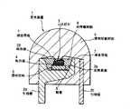
图1所示的剖视图表示现有技术1中公开的发光装置20。该发光装置20包括:容纳在封装(package)21的凹陷部22中的LED芯片23;由光传输树脂制成并嵌入在凹陷部22中的第一涂敷层24和第二涂敷层25;暴露在封装21外部的外部电极26;以及电连接外部电极26和LED芯片23的接合导线27。第二涂敷层25内含磷光体25A,以吸收发自LED芯片23的可见光,并从此发射经波长转换的光。因此,利用发自LED芯片23的波长转换光,可获得不同色彩的可见光。例如,当发自蓝LED芯片23的蓝光穿过内含吸收蓝光的磷光体25A的第二涂敷层25、并随后发射黄光时,蓝光和经波长转换的黄光就混合在一起,由此可获得作为补色的光。The sectional view shown in FIG. 1 shows a light emitting device 20 disclosed in
日本专利申请公开号JP2000-22222(如下称作现有技术2)中公开了另一种发光装置,其中光从与电极形成表面相对的透明衬底侧发射(参见上述专利文献2的图1)。Another light-emitting device is disclosed in Japanese Patent Application Publication No. JP2000-22222 (hereinafter referred to as prior art 2), in which light is emitted from the side of the transparent substrate opposite to the electrode-forming surface (see FIG. 1 of the above-mentioned Patent Document 2) .
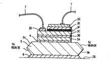
图2所示的剖视图表示现有技术2中公开的发光装置30。该发光装置30包括:一对具有反射角部(reflection horn)31A和31B的引线框31;LED芯片32,其中在诸如蓝宝石之类的透明衬底32A上形成GaN系统发光层32B;设置成与LED芯片32的透明衬底32A接触的波长转换元件33;以及被模制的透明密封材料34,用于覆盖引线框31、LED芯片32和波长转换元件33。The sectional view shown in FIG. 2 shows the
反射角部31A和31B具有接合爪31c和31d,以把波长转换元件33固定在反射框架的整个内圆周上。它们利用接合爪31c和31d压住波长转换元件33的片状基膜34A,以将其牢固地固定。The
LED芯片32具有通过凸起(未示出)与反射角部31A和31B的底部表面31a和31b电连接的电极32a和32b。The LED chip 32 has
波长转换元件33包括基膜33A和形成在基膜33A上的波长转换层33B,该波长转换层33B是通过将波长转换材料与树脂粘合剂均匀混合、涂覆在基膜33A上、之后再硬化而制成的。波长转换元件33设置在反射角部31A和31B中,以使波长转换层33B接触LED芯片32的透明衬底32A,The wavelength conversion element 33 includes a
在这种发光装置中,可通过从LED芯片的透明衬底侧取出光来提高光提取效率。进一步地,把波长转换材料制成层,可提高波长转换的均衡性和效率。因此,显著地降低了由于波长转换的非均匀性而引起的发射色彩不均匀。In such a light emitting device, light extraction efficiency can be improved by taking out light from the transparent substrate side of the LED chip. Furthermore, making the wavelength conversion material into layers can improve the balance and efficiency of wavelength conversion. Therefore, emission color non-uniformity due to non-uniformity of wavelength conversion is significantly reduced.
但是,传统的发光装置存在下列问题:However, conventional lighting devices have the following problems:
(1)在现有技术1所公开的发光装置20中,第二涂敷层25的中心部分制作得比边缘部分厚。因此,磷光体阻碍了光的发射。还有,形成在LED芯片23上的电极(未示出)阻碍光的发射。这样,在导线接合(wire-bonding)结构中,由于光提取效率低,因此难于获得充足的亮度。(1) In the light-emitting device 20 disclosed in
(2)在现有技术2所公开的发光装置30中,在安装LED芯片过程中,需要形成凸起、颠倒粘合表面和定位的步骤。因此,制造过程复杂,而且形成凸起以及定位的步骤需要很高的精度。进一步地,需要昂贵的倒装片粘合剂进行该工艺过程。提高了制造成本。(2) In the light-
因此,现有技术1公开的导线接合结构在制造方面具有优势。但是,现有技术1(导线接合结构)的问题在于,由于降低了光提取效率,而难于获得充足的亮度。Therefore, the wire bonding structure disclosed in
发明内容Contents of the invention
本发明的目的在于提供一种发光装置,该发光装置能够提供很高的光提取效率,同时还具有导线接合结构。The object of the present invention is to provide a light emitting device which can provide high light extraction efficiency and also has a wire bonding structure.
根据本发明的一个方面,一种发光装置包括:According to one aspect of the present invention, a light emitting device includes:
半导体发光元件,该半导体发光元件从设置在与其电极形成表面相对一侧上的其发光表面发射光;a semiconductor light emitting element emitting light from its light emitting surface provided on the side opposite to its electrode forming surface;
引线框,所述引线框通过导线与形成在电极形成表面上的电极电连接,所述引线框中的一个具有杯形体部分,反射表面形成在其内部;lead frames electrically connected to the electrodes formed on the electrode-forming surfaces through wires, one of the lead frames having a cup-shaped body portion inside which the reflective surface is formed;
透明结构,该透明结构与发光表面光连接,并具有基于其三维形状的光分布特性,所述透明结构安装在杯形体部分的底部上,所述半导体发光元件被安装在透明结构上;以及a transparent structure optically connected to the light-emitting surface and having light distribution characteristics based on its three-dimensional shape, said transparent structure being mounted on the bottom of the cup-shaped body portion, said semiconductor light-emitting element being mounted on the transparent structure; and
光传输树脂,该光传输树脂密封半导体发光元件和透明结构;a light-transmitting resin that encapsulates the semiconductor light-emitting element and the transparent structure;
其中,所述半导体发光元件和透明结构容装在杯形体部分中,以允许从所述半导体发光元件、通过透明结构被辐射的光被所述反射表面反射而向上辐射。Wherein, the semiconductor light emitting element and the transparent structure are housed in the cup portion to allow light irradiated from the semiconductor light emitting element through the transparent structure to be reflected by the reflective surface to radiate upward.
根据本发明的另一方面,一种发光装置包括:According to another aspect of the present invention, a light emitting device includes:
半导体发光元件,该半导体发光元件从设置在与其电极形成表面相对一侧上的其发光表面发射光;a semiconductor light emitting element emitting light from its light emitting surface provided on the side opposite to its electrode forming surface;
引线框,所述引线框通过导线与形成在电极形成表面上的电极电连接,所述引线框中的一个具有杯形体部分,反射表面形成在其内部;lead frames electrically connected to the electrodes formed on the electrode-forming surfaces through wires, one of the lead frames having a cup-shaped body portion inside which the reflective surface is formed;
透明结构,该透明结构与发光表面光连接,并具有基于其三维形状的光分布特性,所述透明结构安装在杯形体部分的底部上,所述半导体发光元件被安装在透明结构上;以及a transparent structure optically connected to the light-emitting surface and having light distribution characteristics based on its three-dimensional shape, said transparent structure being mounted on the bottom of the cup-shaped body portion, said semiconductor light-emitting element being mounted on the transparent structure; and
光传输树脂,该光传输树脂密封半导体发光元件和透明结构,该光传输树脂包括磷光体,以对发自该半导体发光元件的光进行波长转换;a light-transmitting resin encapsulating a semiconductor light-emitting element and a transparent structure, the light-transmitting resin including a phosphor to wavelength-convert light emitted from the semiconductor light-emitting element;
其中,所述半导体发光元件和透明结构容装在杯形体部分中,以允许从所述半导体发光元件、通过透明结构被辐射的光被所述反射表面反射而向上辐射。Wherein, the semiconductor light emitting element and the transparent structure are housed in the cup portion to allow light irradiated from the semiconductor light emitting element through the transparent structure to be reflected by the reflective surface to radiate upward.
附图说明Description of drawings
下面参照附图说明根据本发明所述的优选实施例,其中:Illustrate according to the preferred embodiment of the present invention below with reference to accompanying drawing, wherein:
图1所示的横向剖视图表示现有技术1中公开的传统发光装置;The transverse sectional view shown in FIG. 1 shows a conventional light emitting device disclosed in
图2所示的横向剖视图表示现有技术2中公开的另一种发光装置;The transverse sectional view shown in FIG. 2 shows another light emitting device disclosed in prior art 2;
图3所示的横向剖视图表示本发明的第一优选实施例所述的发光装置1。The transverse sectional view shown in Fig. 3 shows the
图4所示的横向剖视图表示第一实施例中所述的部分发光装置。Fig. 4 is a lateral sectional view showing part of the light emitting device described in the first embodiment.
图5所示的横向剖视图表示本发明的第二优选实施例中所述的部分发光装置。The transverse sectional view shown in Fig. 5 shows part of the light emitting device described in the second preferred embodiment of the present invention.
图6所示的横向剖视图表示本发明的第三优选实施例中所述的部分发光装置。The transverse sectional view shown in Fig. 6 shows part of the light emitting device described in the third preferred embodiment of the present invention.
图7所示的横向剖视图表示本发明的第四优选实施例中所述的部分发光装置。Fig. 7 is a transverse sectional view showing part of the light emitting device described in the fourth preferred embodiment of the present invention.
图8所示的横向剖视图表示本发明的第五优选实施例中所述的部分发光装置。Fig. 8 is a transverse sectional view showing part of the light emitting device described in the fifth preferred embodiment of the present invention.
图9所示的横向剖视图表示本发明的第六优选实施例中所述的部分发光装置。The transverse sectional view shown in FIG. 9 shows part of the light emitting device described in the sixth preferred embodiment of the present invention.
图10所示的横向剖视图表示本发明的第七优选实施例中所述的部分发光装置。Fig. 10 is a transverse sectional view showing part of the light emitting device described in the seventh preferred embodiment of the present invention.
图11所示的横向剖视图表示本发明的第八优选实施例中所述的部分发光装置。Fig. 11 is a transverse sectional view showing part of the light emitting device described in the eighth preferred embodiment of the present invention.
图12所示的横向剖视图表示本发明的第九优选实施例中所述的部分发光装置。Fig. 12 is a transverse sectional view showing part of the light emitting device described in the ninth preferred embodiment of the present invention.
图13A和13B所示的俯视图表示本发明的第十优选实施例所述的部分发光装置。13A and 13B are top views showing part of the lighting device according to the tenth preferred embodiment of the present invention.
图14所示的横向剖视图表示本发明的第十一优选实施例所述的部分发光装置。The transverse sectional view shown in Fig. 14 shows part of the light emitting device according to the eleventh preferred embodiment of the present invention.
具体实施方式Detailed ways
图3所示的横向剖视图表示本发明的第一优选实施例所述的发光装置1。该发光装置1包括:由金属材料制成的引线框2A和2C;形成在引线框2A的顶部、以容纳LED芯片3的杯形体2B;通过光传输粘合层4粘合到LED芯片3的透明结构5;把透明结构5固定到杯形体2B底部的银膏(Ag paste)6;电连接在LED芯片3的电极和引线框2A和2C之间的接合导线7;填充在杯形体2B内、以密封LED芯片3和透明结构5的光传输树脂8;以及将引线框2A、2C和接合导线7一体模制的透明环氧树脂9。The transverse sectional view shown in Fig. 3 shows the
引线框2A和2C由诸如具有良好导热性的铜合金之类的金属材料制成。杯形体2B具有形成在其内表面上的反射表面2a。Lead frames 2A and 2C are made of a metal material such as copper alloy having good thermal conductivity. Cup-shaped
例如,LED芯片3为诸如氮化镓(GaN)、氮化铝镓(GaAlN)、氮化镓铟(InGaN)以及氮化铝镓铟(InGaAlN)之类的氮化镓系统化合物的半导体或者为ZnSe(硒化锌),并发射波长为450至480nm的蓝色系统的光。LED芯片3为倒装片粘合式的LED,其中光主要发自位于电极形成表面相对侧上的蓝宝石衬底。透明结构5通过粘合层4粘结到蓝宝石衬底。For example, the
粘合层4用于利用粘合剂使LED芯片3与透明结构5光连接。该粘合层4可以是诸如硅树脂、环氧树脂、丙烯酸树脂和陶瓷膏之类的透明粘合剂。The
透明结构5形成矩形实心体(solid),并是诸如SiO2、Al2O3、SiC、Si3N4、AlN、ZrO2、硼硅玻璃以及铝硅酸盐玻璃之类的光传输材料。其尺寸大于LED芯片3。其厚度范围优选为晶片厚度的一半至晶片较短侧长度的两倍。透明结构5可以是除矩形实心体以外的另一种三维形状。The
光传输树脂8由环氧树脂制成,并含有Ce:YAG(镱-铝-石榴石)作为黄色磷光体。光传输树脂8也可以由硅树脂制成,而不是由环氧树脂制成,该硅树脂在硬化之后变得透明。The light-transmitting
模制透明环氧树脂9,以具有灯的形状,从而会聚从LED芯片3和杯形体2B向上发射的光。The transparent
图4所示的横向剖视图表示第一实施例中的部分发光装置。图4中,环绕LED芯片3的光传输树脂8被省略。该LED芯片3包括:蓝宝石衬底3A;铝缓冲层3B;n型半导体层3C;n电极3D;p型半导体层3E;包括发光层的多层3F;以及p电极3G。接合导线7接合到n电极3D和p电极3G。n电极3D和p电极3G都具有不能使光穿过的厚度。Fig. 4 is a lateral sectional view showing part of the light emitting device in the first embodiment. In FIG. 4, the light-transmitting
在制造发光装置1的过程中,首先,冲压铜合金金属材料,以形成引线框2A和2C的形状;之后,采用压痕法在引线框2A上形成杯形体2B。之后,把透明结构5通过银膏6粘合到杯形体2B。之后,通过提供在其间的粘合层4将LED芯片3粘结到透明结构5。之后,接合接合导线7,以在n电极3D和引线框2A、以及p电极3G和引线框2C之间进行电连接。之后,通过把包括磷光体的环氧树脂注入杯形体2B、并将其硬化,形成光传输树脂8。之后,将光传输树脂8向上移动到金属铸型,在此形成透明环氧树脂9,同时保持引线框2A和2C。之后,在把引线框2A和2C定位到金属铸型、并将其插入金属铸型之后,把透明环氧树脂9注入金属铸型中。环氧树脂硬化之后,将光传输装置1从金属铸型中取出。In the process of manufacturing the light-emitting
在把LED芯片3安装在引线框2A上的过程中,可预先把LED芯片3粘合到透明结构5。例如,如果通过切割片晶片状的基部而形成透明结构5,则LED芯片3就可结合到基部。在此情况下,通过把基部切成预定大小的片,就可获得具有结合为一体的LED芯片3和透明结构5的芯片部分。该芯片部分利用银膏6粘合到引线框2A。在此方式下,可通过一个步骤把LED芯片3和透明结构5同时安装在引线框2A上。In the process of mounting the
下面说明第一实施例所述发光装置的工作过程。The working process of the light emitting device in the first embodiment will be described below.
驱动部分(未示出)向LED芯片3的n电极3D和p电极3G提供驱动电压。多层3F根据驱动电压的大小采用平面发射方式发光。从多层3F发射的光主要穿过蓝宝石衬底3A,进入透明结构5。透明结构5反射进入其内的部分光,之后,将这部分光从其侧部表面和靠近粘合表面的上表面射(discharging)到LED芯片3。从透明结构5射出的部分光作用到光传输树脂8内的磷光体上。磷光体被所提供的光激发,并发射出波成为550至580nm的被激发的光。这种被激发的光与从透明结构5发射出的光混合,以提供白光。白光在杯形体2B的反射表面2a上被反射,并随后向上发射到透明环氧树脂9。A drive section (not shown) supplies a drive voltage to n-
第一实施例中的上述发光装置具有如下效果。The above-described light emitting device in the first embodiment has the following effects.
(1)由于矩形实心体的透明结构5利用粘合层4粘合到蓝宝石衬底,并被固定到杯形体2B,因此可很容易地通过接合导线7将LED芯片3连接到引线框2A和2C。进一步地,由于在倒装片粘合的情况下并不需要在凸起形成步骤或者LED芯片安装步骤中所要求的准确定位,因此可以简化制造过程。采用这种简化的制造过程,可降低制造成本,并且可以提高生产率。(1) Since the
(2)由于通过透明结构5发射光,因此可降低发光密度,并且光本身可以获得不同于LED芯片3的光分布特性的光分布特性。因此,可将光有效地提供到光传输树脂8中的磷光体。正因如此,使经波长转换的黄光与蓝光均匀混合,从而可避免发射色彩不均匀。(2) Since the light is emitted through the
(3)由于发光区域因透明结构5而放大,因此降低了由于磷光体覆盖LED芯片而引起的光屏蔽效应,进而提高了亮度。(3) Since the light-emitting area is enlarged by the
尽管在上述第一实施例中,发光装置1使用不透明的n电极3D和p电极3G,然而,n电极3D和p电极3G也可以是透明的,而且LED芯片3可设有透明衬底。Although in the first embodiment described above, the
图5所示的横向剖视图表示本发明的第二优选实施例中的部分发光装置。与第一实施例所述的发光装置1不同,第二实施例所述的发光装置1是这样组成的,即透明结构5利用粘合层4A(包括粘合树脂)粘合到杯形体2B,同时铝等白色填充物4a混合作为光漫射材料。由第一实施例中使用的相同附图标记表示相同的部件,而且在下面省略了对其说明。The transverse sectional view shown in Fig. 5 shows part of the light emitting device in the second preferred embodiment of the present invention. Unlike the light-emitting
在第二实施例中,除第一实施例的效果之外,还可利用混合到粘合层4A中的光漫射材料改变位于透明结构5底部处的光漫射特性。更进一步地,通过使用具有混合在其内的白色填充物的粘合树脂(白色膏)或者透明粘合树脂(透明膏)代替银膏6,而实现长期稳定的亮度。这是因为,在使用银膏的情况下,银填充物由于加热或者由于发自LED的光而被氧化,而且反射率随时间而衰退。In the second embodiment, in addition to the effects of the first embodiment, the light-diffusing property at the bottom of the
图6所示的横向剖视图表示本发明的第三优选实施例中所述的部分发光装置。与第二实施例所述的发光装置1不同,第三实施例所述的发光装置1是这样组成的,即透明结构5利用具有黄色磷光体4b的粘合层4A(包括粘合树脂)而被粘合到杯形体2B,该黄色磷光体4b与包含在混合于其内的光传输树脂8中的类型相同。由第二实施例中使用的相同附图标记表示相同的部件,而且在下面省略了对其的说明。The transverse sectional view shown in Fig. 6 shows part of the light emitting device described in the third preferred embodiment of the present invention. Unlike the light-emitting
在第三实施例中,除了达到第一实施例的效果之外,还可以从粘合层4A中的黄色磷光体4b发射被激发的光。因此,可减少混合在光传输树脂8中的磷光体的量,并进而进一步提高光提取(extraction)效率,以增加亮度。这是因为可减少由混合在光传输树脂8中的磷光体引起的光屏蔽效应。进一步地,可进一步地提高在透明结构5底部处的光漫射特性。In the third embodiment, in addition to achieving the effects of the first embodiment, excited light can be emitted from the yellow phosphor 4b in the
图7所示的横向剖视图表示本发明的第四优选实施例中所述的部分发光装置。与第二实施例所述的发光装置1不同,第四实施例所述的发光装置1是这样组成的,即LED芯片3发射波长大约为380nm的紫外光,将被紫外光激发的红色磷光体4c、蓝色磷光体4d和绿色磷光体4e用于发射白光,红色磷光体4c混合在粘合层4中,而蓝色磷光体4d和绿色磷光体混合在光传输树脂8内。由第一和第二实施例中使用的相同附图标记表示相同的部件,而且在下面省略了对其的说明。Fig. 7 is a transverse sectional view showing part of the light emitting device described in the fourth preferred embodiment of the present invention. Different from the light-emitting
红色磷光体4c例如是Y(P,V)O4:Eu或者Y2O2S:Eu。The red phosphor 4 c is, for example, Y(P,V)O4 :Eu or Y2 O2 S:Eu.
蓝色磷光体4d例如是(Ba,Ca,Mg)10(PO4)6C12:Eu或者Sr2P2O7:Eu。The
绿色磷光体4e例如是(Ba,Mg)2Al16C27:Eu或者BaMgAl16C27:Eu。The
在第四实施例中,除了达到第一实施例的效果之外,通过将具有最低激发效率的红色磷光体4c混合到粘合层4A中,可降低混合在光传输树脂8中的磷光体的量,从而进一步提高光提取(extraction)效率,以增加亮度。对于磷光体的沉积,可有选择地把红色、蓝色和绿色磷光体中的至少一种混合到粘合层4A中,而其余的磷光体混合到光传输树脂8。并且,红色、蓝色和绿色磷光体可混合到光传输树脂8中。In the fourth embodiment, in addition to achieving the effect of the first embodiment, by mixing the red phosphor 4c having the lowest excitation efficiency into the
图8所示的横向剖视图表示本发明的第五优选实施例中所述的部分发光装置。与第一实施例所述的发光装置1不同,第五实施例所述的发光装置1是这样组成的,即透明结构5具有形成在底部处的微观的不平坦表面5A,并提供厚度大约为1500埃的反射膜5B作为铝膜。由第一实施例中使用的相同附图标记表示相同的部件,而且在下面省略了对其的说明。Fig. 8 is a transverse sectional view showing part of the light emitting device described in the fifth preferred embodiment of the present invention. Unlike the
在第五实施例中,除了达到第一实施例的效果之外,还可根据微观不平坦表面5A和光反射膜5B的形状,进一步提高透明结构5底部的光漫射特性和反射率。进一步地,由于透明结构5具有光漫射结构和光反光膜,因此可使用银膏把透明结构5粘合到杯形体2B。In the fifth embodiment, in addition to achieving the effect of the first embodiment, the light diffusion and reflectivity of the bottom of the
图9所示的横向剖视图表示本发明的第六优选实施例中所述的部分发光装置。与第一实施例所述的发光装置1不同,第六实施例所述的发光装置1是这样组成的,即透明结构5具有四个倾斜面5a,这些倾斜面5a具有梯形横截面,以在前、后、左、右方向上扩大其底部部分。由第一实施例中使用的相同附图标记表示相同的部件,而且在下面省略了对其的说明。The transverse sectional view shown in FIG. 9 shows part of the light emitting device described in the sixth preferred embodiment of the present invention. Different from the light-emitting
在第六实施例中,除了达到第一实施例的效果之外,还可根据倾斜面5a的形状,在水平和垂直方向上有效地发射光。就像第三实施例中描述的那样,透明结构5可在底部具有微观不平坦表面和光反射表面。In the sixth embodiment, in addition to the effects of the first embodiment, light can be efficiently emitted in the horizontal and vertical directions according to the shape of the
图10所示的横向剖视图表示本发明的第七优选实施例中所述的部分发光装置。与第六实施例所述的发光装置1不同,第七实施例所述的发光装置1是这样组成的,即透明结构5具有四个倾斜面5a,这些倾斜面5a具有倒置的梯形横截面,以在前、后、左、右方向上扩大其顶部部分。由第六实施例中使用的相同附图标记表示相同的部件,而且在下面省略了对其的说明。Fig. 10 is a transverse sectional view showing part of the light emitting device described in the seventh preferred embodiment of the present invention. Different from the light-emitting
在第七实施例中,除了达到第一实施例的效果之外,通过使反射光传输穿过在倾斜面5a上的透明结构5,可向上有效地发射光。就像第三实施例中所述的那样,透明结构5可在底部处具有微观不平坦表面和光反射表面。In the seventh embodiment, in addition to achieving the effect of the first embodiment, light can be efficiently emitted upward by transmitting reflected light through the
图11所示的横向剖视图表示本发明的第八优选实施例中所述的部分发光装置。与第六实施例所述的发光装置1不同,第八实施例所述的发光装置1是这样组成的,即透明结构5具有四个倾斜面5b和5c,这些倾斜面具有五边形横截面,以在前、后、左、右方向上扩大其中心部分。由第六实施例中使用的相同附图标记表示相同的部件,而且在下面省略了对其的说明。Fig. 11 is a transverse sectional view showing part of the light emitting device described in the eighth preferred embodiment of the present invention. Unlike the light-emitting
在第八实施例中,除了达到第一实施例的效果之外,还可根据倾斜面5b和5c的形状,在水平和垂直方向上有效地发射光。就像第三实施例所描述的那样,透明结构5可在底部处具有微观不平坦表面和光反射表面。In the eighth embodiment, in addition to the effects of the first embodiment, light can be efficiently emitted in the horizontal and vertical directions according to the shapes of the
图12所示的横向剖视图表示本发明的第九优选实施例中所述的部分发光装置。与第一实施例所述的发光装置1不同,第九实施例所述的发光装置1是这样组成的,即透明结构5具有位于底部中心的凹陷表面和形成在凹陷表面上的反射膜5B。由第一实施例中使用的相同附图标记表示相同的部件,而且在下面省略了对其的说明。Fig. 12 is a transverse sectional view showing part of the light emitting device described in the ninth preferred embodiment of the present invention. Unlike the
反射膜5B例如为采用沉积方法形成的铝膜,并优选具有有效的反射率和不平坦度,以漫射光。The reflective film 5B is, for example, an aluminum film formed by a deposition method, and preferably has effective reflectivity and unevenness to diffuse light.
在第九实施例中,除了达到第一实施例的效果之外,还可通过使反射光进入反射膜5B上的透明结构5,而使光可有效地从透明结构5的侧部表面向上反射。就像第四和第五实施例所述的那样,可使透明结构5形成为具有梯形的横截面,从而可提高水平和垂直方向上的光提取效率。In the ninth embodiment, in addition to achieving the effects of the first embodiment, light can be effectively reflected upward from the side surface of the
图13A至13C所示的俯视图表示本发明的第十优选实施例所述的部分发光装置。尽管在第一至第九实施例中,透明结构5具有矩形实心形状或梯形横截面,如图13A所示,但也可以具有其他形状。例如,可以是如图13B所示的圆形或者如图13C所示的八边形,或者根据所需的光分布特性或用途而具有另一种形状。13A to 13C are plan views showing part of the lighting device according to the tenth preferred embodiment of the present invention. Although in the first to ninth embodiments, the
图14所示的横向剖视图表示本发明的第十一优选实施例所述的部分发光装置。在第十一实施例中,LED芯片3通过粘合层4粘合到透明结构5,而且LED芯片3通过金凸起(bump)11A和11B采用倒装片方式安装在辅助安装(submount)元件10上。采用设置在上述LED芯片3之上的透明结构5,可提高光提取效率。由第一实施例中使用的相同附图标记表示相同的部件,而且在下面省略了对其的说明。The transverse sectional view shown in Fig. 14 shows part of the light emitting device according to the eleventh preferred embodiment of the present invention. In the eleventh embodiment, the
辅助安装件10为n型硅衬底,并作为齐纳(Zener)二极管工作,以保护LED芯片3免于静电干扰。该辅助安装件10还包括:通过金凸起11A与p电极3G连接的n电极10A;p型半导体层10B;通过金凸起11B与n电极3D连接的p电极10C;通过银膏6与杯形体2B电连接的n电极10D;以及n型半导体层10E。The auxiliary mounting
在第十一实施例中,LED芯片3的光射出(discharging)表面采用倒装片粘合方式设置在杯形体2B的开口侧,而透明结构5粘合到蓝宝石衬底3A的表面,作为光射出表面。因此,可从透明结构5的侧表面、底表面和顶表面取出光,并由此可扩大光射出面积。In the eleventh embodiment, the light emitting (discharging) surface of the
在具有经倒装片粘合的LED芯片3的发光装置中,由于粘合到LED芯片3的光射出表面的透明结构5,可减少由于磷光体覆盖光源而引起的光屏蔽效应。透明结构5可形成为在其上部具有灯形状,以提供将光向上垂直会聚的特性。In a light emitting device with flip-chip bonded
尽管在上述实施例中,发光装置1安装在引线框上,但它也可以安装在衬底(电路板)上。Although in the above-described embodiments, the
磷光体可包含在透明环氧树脂9中,而不是包含在光传输树脂8中。可供选择地,磷光体可以不包含在任何透明环氧树脂9和光传输树脂8中。Phosphors may be contained in transparent
LED芯片3可发射除蓝色以外的红色或绿色可见光、或者紫外光。可根据将被发射的光,选择将被激发的磷光体。The
尽管为完整而清楚地描述其内容,已参照具体实施例说明了本发明,但是,随附权利要求并不受这种限制,对于本领域的技术人员来说,这些权利要求将被解释为包括合理地落入本文的上述基本教导之内的所有改进和可选的结构。While the invention has been described with reference to specific embodiments for completeness and clarity of description, the appended claims are not so limited and will be construed to those skilled in the art to include All modifications and alternative constructions reasonably fall within the above basic teachings herein.
Claims (8)
Translated fromChineseApplications Claiming Priority (2)
| Application Number | Priority Date | Filing Date | Title |
|---|---|---|---|
| JP2003043109AJP4254266B2 (en) | 2003-02-20 | 2003-02-20 | LIGHT EMITTING DEVICE AND LIGHT EMITTING DEVICE MANUFACTURING METHOD |
| JP2003043109 | 2003-02-20 |
Publications (2)
| Publication Number | Publication Date |
|---|---|
| CN1523683A CN1523683A (en) | 2004-08-25 |
| CN100411198Ctrue CN100411198C (en) | 2008-08-13 |
Family
ID=32866451
Family Applications (1)
| Application Number | Title | Priority Date | Filing Date |
|---|---|---|---|
| CNB2004100053698AExpired - Fee RelatedCN100411198C (en) | 2003-02-20 | 2004-02-11 | light emitting device |
Country Status (4)
| Country | Link |
|---|---|
| US (1) | US20040164311A1 (en) |
| JP (1) | JP4254266B2 (en) |
| KR (1) | KR100710102B1 (en) |
| CN (1) | CN100411198C (en) |
Families Citing this family (77)
| Publication number | Priority date | Publication date | Assignee | Title |
|---|---|---|---|---|
| US7880182B2 (en)* | 2002-07-15 | 2011-02-01 | Epistar Corporation | Light-emitting element array |
| TWI249148B (en)* | 2004-04-13 | 2006-02-11 | Epistar Corp | Light-emitting device array having binding layer |
| US7915085B2 (en)* | 2003-09-18 | 2011-03-29 | Cree, Inc. | Molded chip fabrication method |
| JP4516337B2 (en)* | 2004-03-25 | 2010-08-04 | シチズン電子株式会社 | Semiconductor light emitting device |
| US6849876B1 (en)* | 2004-05-31 | 2005-02-01 | Excel Cell Electronic Co., Ltd. | Light emitting device |
| US7361938B2 (en)* | 2004-06-03 | 2008-04-22 | Philips Lumileds Lighting Company Llc | Luminescent ceramic for a light emitting device |
| US20060091414A1 (en)* | 2004-10-29 | 2006-05-04 | Ouderkirk Andrew J | LED package with front surface heat extractor |
| US7304425B2 (en)* | 2004-10-29 | 2007-12-04 | 3M Innovative Properties Company | High brightness LED package with compound optical element(s) |
| US7329982B2 (en)* | 2004-10-29 | 2008-02-12 | 3M Innovative Properties Company | LED package with non-bonded optical element |
| US20060091412A1 (en)* | 2004-10-29 | 2006-05-04 | Wheatley John A | Polarized LED |
| TWI252597B (en)* | 2004-12-02 | 2006-04-01 | Formosa Epitaxy Inc | Light emitting diode package |
| CN100416871C (en)* | 2004-12-09 | 2008-09-03 | 璨圆光电股份有限公司 | Light emitting diode packaging structure |
| US20060131708A1 (en)* | 2004-12-16 | 2006-06-22 | Ng Kee Y | Packaged electronic devices, and method for making same |
| KR100638666B1 (en)* | 2005-01-03 | 2006-10-30 | 삼성전기주식회사 | Nitride semiconductor light emitting device |
| TWI352437B (en) | 2007-08-27 | 2011-11-11 | Epistar Corp | Optoelectronic semiconductor device |
| US7598663B2 (en)* | 2005-08-04 | 2009-10-06 | Taiwan Oasis Technology Co., Ltd. | Multi-wavelength LED provided with combined fluorescent materials positioned over and underneath the LED component |
| EP1928030B1 (en) | 2005-09-20 | 2019-01-30 | Panasonic Intellectual Property Management Co., Ltd. | Led lighting fixture |
| CN1331245C (en)* | 2005-09-30 | 2007-08-08 | 晶能光电(江西)有限公司 | InGaAlN luminescent device |
| US20070080636A1 (en)* | 2005-10-07 | 2007-04-12 | Taiwan Oasis Technology Co., Ltd. | White multi-wavelength LED & its manufacturing process |
| KR100713180B1 (en)* | 2005-11-21 | 2007-05-04 | (주)루멘스 | Side-emitting type light emitting diode package and manufacturing method thereof |
| US20070141749A1 (en)* | 2005-12-20 | 2007-06-21 | Yi-Fong Lin | Die attachment method for LED chip and structure thereof |
| DE102006005042A1 (en)* | 2006-02-03 | 2007-08-09 | Tridonic Optoelectronics Gmbh | Light-emitting device with non-activated phosphor |
| US7586125B2 (en)* | 2006-02-20 | 2009-09-08 | Industrial Technology Research Institute | Light emitting diode package structure and fabricating method thereof |
| DE102006042061A1 (en)* | 2006-09-05 | 2008-03-27 | Noctron Holding S.A. | Semiconductor-illuminant has semiconductor-diode which is illuminated by tension admission, and substrate which is permeable for light produced by semiconductor-diode |
| US7863639B2 (en)* | 2006-04-12 | 2011-01-04 | Semileds Optoelectronics Co. Ltd. | Light-emitting diode lamp with low thermal resistance |
| US8373195B2 (en) | 2006-04-12 | 2013-02-12 | SemiLEDs Optoelectronics Co., Ltd. | Light-emitting diode lamp with low thermal resistance |
| US20070257270A1 (en)* | 2006-05-02 | 2007-11-08 | 3M Innovative Properties Company | Led package with wedge-shaped optical element |
| US7525126B2 (en) | 2006-05-02 | 2009-04-28 | 3M Innovative Properties Company | LED package with converging optical element |
| US7390117B2 (en)* | 2006-05-02 | 2008-06-24 | 3M Innovative Properties Company | LED package with compound converging optical element |
| US20070257271A1 (en)* | 2006-05-02 | 2007-11-08 | 3M Innovative Properties Company | Led package with encapsulated converging optical element |
| US7953293B2 (en)* | 2006-05-02 | 2011-05-31 | Ati Technologies Ulc | Field sequence detector, method and video device |
| WO2008011377A2 (en)* | 2006-07-17 | 2008-01-24 | 3M Innovative Properties Company | Led package with converging extractor |
| US20080042157A1 (en)* | 2006-08-16 | 2008-02-21 | Formosa Epitaxy Incorporation | Surface mount light emitting diode package |
| US7910938B2 (en) | 2006-09-01 | 2011-03-22 | Cree, Inc. | Encapsulant profile for light emitting diodes |
| US8425271B2 (en)* | 2006-09-01 | 2013-04-23 | Cree, Inc. | Phosphor position in light emitting diodes |
| WO2008060586A2 (en) | 2006-11-15 | 2008-05-22 | The Regents Of The University Of California | Textured phosphor conversion layer light emitting diode |
| WO2008060584A2 (en)* | 2006-11-15 | 2008-05-22 | The Regents Of The University Of California | High light extraction efficiency sphere led |
| US20090121250A1 (en)* | 2006-11-15 | 2009-05-14 | Denbaars Steven P | High light extraction efficiency light emitting diode (led) using glass packaging |
| DE202006017583U1 (en)* | 2006-11-17 | 2008-03-27 | Patent-Treuhand-Gesellschaft für elektrische Glühlampen mbH | lighting device |
| US7521862B2 (en)* | 2006-11-20 | 2009-04-21 | Philips Lumileds Lighting Co., Llc | Light emitting device including luminescent ceramic and light-scattering material |
| JP2010512662A (en) | 2006-12-11 | 2010-04-22 | ザ リージェンツ オブ ザ ユニバーシティ オブ カリフォルニア | Transparent light emitting diode |
| US7902564B2 (en)* | 2006-12-22 | 2011-03-08 | Koninklijke Philips Electronics N.V. | Multi-grain luminescent ceramics for light emitting devices |
| KR101334314B1 (en)* | 2006-12-28 | 2013-11-28 | 서울반도체 주식회사 | Light emitting diode lamp and method of fabricating the same |
| US20080173890A1 (en)* | 2007-01-19 | 2008-07-24 | Wen-Kung Sung | Multidirectional light-emitting diode |
| US9024349B2 (en) | 2007-01-22 | 2015-05-05 | Cree, Inc. | Wafer level phosphor coating method and devices fabricated utilizing method |
| US9159888B2 (en)* | 2007-01-22 | 2015-10-13 | Cree, Inc. | Wafer level phosphor coating method and devices fabricated utilizing method |
| US20080246044A1 (en)* | 2007-04-09 | 2008-10-09 | Siew It Pang | LED device with combined Reflector and Spherical Lens |
| US9041285B2 (en) | 2007-12-14 | 2015-05-26 | Cree, Inc. | Phosphor distribution in LED lamps using centrifugal force |
| US8878219B2 (en)* | 2008-01-11 | 2014-11-04 | Cree, Inc. | Flip-chip phosphor coating method and devices fabricated utilizing method |
| JP5183247B2 (en)* | 2008-02-25 | 2013-04-17 | 京セラ株式会社 | Light emitting device |
| KR100903280B1 (en)* | 2008-10-13 | 2009-06-17 | 최운용 | LED assembly having redundancy electrode and manufacturing method thereof |
| CN102341923B (en)* | 2008-10-13 | 2013-09-18 | 崔云龙 | LED device with redundant electrodes and manufacturing method thereof |
| KR101585102B1 (en)* | 2009-04-16 | 2016-01-13 | 삼성전자 주식회사 | Light emitting device and method of manufacturing |
| KR101034054B1 (en)* | 2009-10-22 | 2011-05-12 | 엘지이노텍 주식회사 | Light emitting device package and manufacturing method thereof |
| JP5047264B2 (en) | 2009-12-22 | 2012-10-10 | 株式会社東芝 | Light emitting device |
| JP5050045B2 (en)* | 2009-12-22 | 2012-10-17 | 株式会社東芝 | Light emitting device |
| WO2011152262A1 (en) | 2010-05-31 | 2011-12-08 | 日亜化学工業株式会社 | Light-emitting device and manufacturing method therefor |
| US10546846B2 (en) | 2010-07-23 | 2020-01-28 | Cree, Inc. | Light transmission control for masking appearance of solid state light sources |
| KR20120088130A (en)* | 2011-01-31 | 2012-08-08 | 서울반도체 주식회사 | Light emitting device having wavelength converting layer and method of fabricating the same |
| US9166126B2 (en) | 2011-01-31 | 2015-10-20 | Cree, Inc. | Conformally coated light emitting devices and methods for providing the same |
| US20120256205A1 (en)* | 2011-04-06 | 2012-10-11 | Tek Beng Low | Led lighting module with uniform light output |
| KR101772588B1 (en) | 2011-08-22 | 2017-09-13 | 한국전자통신연구원 | MIT device molded by Clear compound epoxy and fire detecting device including the MIT device |
| KR101294711B1 (en) | 2012-03-02 | 2013-08-08 | 주식회사 세미콘라이트 | Semiconductor light emimitting device |
| WO2013179625A1 (en)* | 2012-05-31 | 2013-12-05 | パナソニック株式会社 | Led module and production method therefor, lighting device |
| JP6062431B2 (en)* | 2012-06-18 | 2017-01-18 | シャープ株式会社 | Semiconductor light emitting device |
| JP2014175354A (en)* | 2013-03-06 | 2014-09-22 | Disco Abrasive Syst Ltd | Light-emitting diode |
| JP2014225636A (en)* | 2013-04-16 | 2014-12-04 | 株式会社ディスコ | Light-emitting device |
| JP2015008274A (en)* | 2013-05-31 | 2015-01-15 | 株式会社ディスコ | Light emitting chip |
| JP2015012212A (en)* | 2013-07-01 | 2015-01-19 | 株式会社ディスコ | Light emitting chip |
| JP6255235B2 (en)* | 2013-12-20 | 2017-12-27 | 株式会社ディスコ | Light emitting chip |
| KR20150096198A (en)* | 2014-02-14 | 2015-08-24 | 삼성전자주식회사 | Light Emitting Device Package and Method for Fabricating the Same |
| CN111917001B (en)* | 2019-05-07 | 2021-07-23 | 光宝光电(常州)有限公司 | Light source device |
| US11205731B2 (en) | 2019-05-07 | 2021-12-21 | Lite-On Opto Technology (Changzhou) Co., Ltd. | Light source package structure |
| JP7226146B2 (en)* | 2019-07-03 | 2023-02-21 | 豊田合成株式会社 | illumination device |
| US11592166B2 (en) | 2020-05-12 | 2023-02-28 | Feit Electric Company, Inc. | Light emitting device having improved illumination and manufacturing flexibility |
| US11876042B2 (en) | 2020-08-03 | 2024-01-16 | Feit Electric Company, Inc. | Omnidirectional flexible light emitting device |
| KR20240101952A (en)* | 2021-11-18 | 2024-07-02 | 루미레즈 엘엘씨 | LED (LIGHT-EMITTING DIODE) package and manufacturing method with reflective coating |
Citations (4)
| Publication number | Priority date | Publication date | Assignee | Title |
|---|---|---|---|---|
| JP2001217467A (en)* | 2000-02-02 | 2001-08-10 | Ind Technol Res Inst | High efficiency white light emitting diode |
| CN1319259A (en)* | 1999-07-29 | 2001-10-24 | 西铁城电子股份有限公司 | led |
| US6310364B1 (en)* | 1998-08-03 | 2001-10-30 | Toyoda Gosei Co., Ltd. | Light-emitting apparatus |
| JP2002176201A (en)* | 2000-12-05 | 2002-06-21 | Okaya Electric Ind Co Ltd | Semiconductor light emitting element |
Family Cites Families (13)
| Publication number | Priority date | Publication date | Assignee | Title |
|---|---|---|---|---|
| DE19600306C1 (en)* | 1996-01-05 | 1997-04-10 | Siemens Ag | Semiconductor component with hermetically-sealed housing for opto-electronic component |
| JP3505405B2 (en)* | 1998-10-22 | 2004-03-08 | 三洋電機株式会社 | Semiconductor device and method of manufacturing the same |
| US6351069B1 (en)* | 1999-02-18 | 2002-02-26 | Lumileds Lighting, U.S., Llc | Red-deficiency-compensating phosphor LED |
| JP2001007389A (en) | 1999-06-21 | 2001-01-12 | Toshiba Corp | Method for manufacturing semiconductor light emitting device |
| JP4066620B2 (en)* | 2000-07-21 | 2008-03-26 | 日亜化学工業株式会社 | LIGHT EMITTING ELEMENT, DISPLAY DEVICE HAVING LIGHT EMITTING ELEMENT AND METHOD FOR MANUFACTURING DISPLAY DEVICE |
| US6791119B2 (en)* | 2001-02-01 | 2004-09-14 | Cree, Inc. | Light emitting diodes including modifications for light extraction |
| US20020117672A1 (en) | 2001-02-23 | 2002-08-29 | Ming-Sung Chu | High-brightness blue-light emitting crystalline structure |
| TW525278B (en)* | 2001-03-15 | 2003-03-21 | Opto Tech Corp | Package structure of high-efficiency electro-optical device and the forming method thereof |
| TW480749B (en)* | 2001-03-15 | 2002-03-21 | Opto Tech Corp | Structure and fabrication method for electro-optics device |
| JP2002299698A (en) | 2001-03-30 | 2002-10-11 | Sumitomo Electric Ind Ltd | Light emitting device |
| TW543128B (en)* | 2001-07-12 | 2003-07-21 | Highlink Technology Corp | Surface mounted and flip chip type LED package |
| US6571033B2 (en)* | 2001-09-28 | 2003-05-27 | Corning Incorporated | Optical signal device |
| KR100554453B1 (en)* | 2002-08-21 | 2006-03-03 | 서울반도체 주식회사 | White light emitting device |
- 2003
- 2003-02-20JPJP2003043109Apatent/JP4254266B2/ennot_activeExpired - Fee Related
- 2004
- 2004-02-10USUS10/774,389patent/US20040164311A1/ennot_activeAbandoned
- 2004-02-11CNCNB2004100053698Apatent/CN100411198C/ennot_activeExpired - Fee Related
- 2004-02-19KRKR1020040010861Apatent/KR100710102B1/ennot_activeExpired - Fee Related
Patent Citations (4)
| Publication number | Priority date | Publication date | Assignee | Title |
|---|---|---|---|---|
| US6310364B1 (en)* | 1998-08-03 | 2001-10-30 | Toyoda Gosei Co., Ltd. | Light-emitting apparatus |
| CN1319259A (en)* | 1999-07-29 | 2001-10-24 | 西铁城电子股份有限公司 | led |
| JP2001217467A (en)* | 2000-02-02 | 2001-08-10 | Ind Technol Res Inst | High efficiency white light emitting diode |
| JP2002176201A (en)* | 2000-12-05 | 2002-06-21 | Okaya Electric Ind Co Ltd | Semiconductor light emitting element |
Also Published As
| Publication number | Publication date |
|---|---|
| CN1523683A (en) | 2004-08-25 |
| KR20040075738A (en) | 2004-08-30 |
| KR100710102B1 (en) | 2007-04-23 |
| JP2004253651A (en) | 2004-09-09 |
| JP4254266B2 (en) | 2009-04-15 |
| US20040164311A1 (en) | 2004-08-26 |
Similar Documents
| Publication | Publication Date | Title |
|---|---|---|
| CN100411198C (en) | light emitting device | |
| KR101521260B1 (en) | Light emitting diode package and manufacturing method thereof | |
| US10141491B2 (en) | Method of manufacturing light emitting device | |
| US7842526B2 (en) | Light emitting device and method of producing same | |
| CN101315966B (en) | Optical semiconductor device | |
| US9425367B2 (en) | Light emitting device having opening for extracting light and method for manufacturing light emitting device having opening for extracting light | |
| CN100440555C (en) | Light emitting device and manufacturing method thereof | |
| US10326060B2 (en) | Light emitting device | |
| US8946749B2 (en) | Semiconductor light emitting device | |
| TWI484666B (en) | Illuminating device | |
| US20140151734A1 (en) | Light-emitting device and method for manufacturing same | |
| JP5644352B2 (en) | Light emitting device and manufacturing method thereof | |
| CN102113139A (en) | Light-emitting device | |
| CN101800281A (en) | semiconductor light-emitting apparatus | |
| JP5527456B2 (en) | Method for manufacturing light emitting device | |
| JP2004343059A (en) | Semiconductor device and manufacturing method thereof | |
| JP2007335798A (en) | Light-emitting device | |
| JP7236016B2 (en) | light emitting device | |
| JP2001177157A (en) | Semiconductor light emitting device | |
| CN104425701A (en) | Light emitting device | |
| CN102263191B (en) | Light emitting device package | |
| JP3994094B2 (en) | Light emitting diode lamp | |
| JP2020053604A (en) | Light-emitting device and manufacturing method thereof | |
| JP5949875B2 (en) | Light emitting device and manufacturing method thereof | |
| JP2009177188A (en) | Light emitting diode package |
Legal Events
| Date | Code | Title | Description |
|---|---|---|---|
| C06 | Publication | ||
| PB01 | Publication | ||
| C10 | Entry into substantive examination | ||
| SE01 | Entry into force of request for substantive examination | ||
| C14 | Grant of patent or utility model | ||
| GR01 | Patent grant | ||
| C17 | Cessation of patent right | ||
| CF01 | Termination of patent right due to non-payment of annual fee | Granted publication date:20080813 Termination date:20100211 |