CN100411180C - Semiconductor structure and method of manufacturing semiconductor structure - Google Patents
Semiconductor structure and method of manufacturing semiconductor structureDownload PDFInfo
- Publication number
- CN100411180C CN100411180CCNB2006100024675ACN200610002467ACN100411180CCN 100411180 CCN100411180 CCN 100411180CCN B2006100024675 ACNB2006100024675 ACN B2006100024675ACN 200610002467 ACN200610002467 ACN 200610002467ACN 100411180 CCN100411180 CCN 100411180C
- Authority
- CN
- China
- Prior art keywords
- semiconductor
- region
- doped region
- semiconductor material
- crystal orientation
- Prior art date
- Legal status (The legal status is an assumption and is not a legal conclusion. Google has not performed a legal analysis and makes no representation as to the accuracy of the status listed.)
- Expired - Fee Related
Links
- 239000004065semiconductorSubstances0.000titleclaimsabstractdescription226
- 238000004519manufacturing processMethods0.000titleclaimsdescription4
- 238000000034methodMethods0.000claimsabstractdescription62
- 239000013078crystalSubstances0.000claimsabstractdescription61
- 239000000758substrateSubstances0.000claimsabstractdescription61
- 239000000463materialSubstances0.000claimsdescription94
- 238000005530etchingMethods0.000claimsdescription17
- 230000005669field effectEffects0.000claimsdescription13
- 238000002955isolationMethods0.000claimsdescription9
- 229910000577Silicon-germaniumInorganic materials0.000claimsdescription7
- 239000002019doping agentSubstances0.000claimsdescription7
- 238000005468ion implantationMethods0.000claimsdescription5
- 229910003811SiGeCInorganic materials0.000claimsdescription4
- 229910003465moissaniteInorganic materials0.000claimsdescription4
- 229910010271silicon carbideInorganic materials0.000claimsdescription4
- 229910001218Gallium arsenideInorganic materials0.000claimsdescription3
- 229910000927Ge alloyInorganic materials0.000claimsdescription3
- 229910000673Indium arsenideInorganic materials0.000claimsdescription3
- 150000001875compoundsChemical class0.000claimsdescription3
- 230000000694effectsEffects0.000claimsdescription3
- 238000011065in-situ storageMethods0.000claimsdescription3
- RPQDHPTXJYYUPQ-UHFFFAOYSA-Nindium arsenideChemical compound[In]#[As]RPQDHPTXJYYUPQ-UHFFFAOYSA-N0.000claimsdescription3
- 239000012212insulatorSubstances0.000abstractdescription4
- 235000012431wafersNutrition0.000description29
- XUIMIQQOPSSXEZ-UHFFFAOYSA-NSiliconChemical compound[Si]XUIMIQQOPSSXEZ-UHFFFAOYSA-N0.000description12
- 229910052710siliconInorganic materials0.000description12
- 239000010703siliconSubstances0.000description12
- 125000006850spacer groupChemical group0.000description7
- 150000004767nitridesChemical class0.000description4
- 238000001020plasma etchingMethods0.000description4
- 238000005229chemical vapour depositionMethods0.000description3
- 239000004020conductorSubstances0.000description3
- 238000009792diffusion processMethods0.000description3
- 238000010438heat treatmentMethods0.000description3
- 229920002120photoresistant polymerPolymers0.000description3
- 239000000126substanceSubstances0.000description3
- -1N2Inorganic materials0.000description2
- 230000015556catabolic processEffects0.000description2
- 238000006731degradation reactionMethods0.000description2
- 238000011049fillingMethods0.000description2
- 238000000227grindingMethods0.000description2
- 229910052739hydrogenInorganic materials0.000description2
- 239000001257hydrogenSubstances0.000description2
- 230000000873masking effectEffects0.000description2
- 230000003647oxidationEffects0.000description2
- 238000007254oxidation reactionMethods0.000description2
- 230000003071parasitic effectEffects0.000description2
- 238000005498polishingMethods0.000description2
- UFHFLCQGNIYNRP-UHFFFAOYSA-NHydrogenChemical compound[H][H]UFHFLCQGNIYNRP-UHFFFAOYSA-N0.000description1
- 229910045601alloyInorganic materials0.000description1
- 239000000956alloySubstances0.000description1
- 230000004888barrier functionEffects0.000description1
- 230000015572biosynthetic processEffects0.000description1
- 239000013590bulk materialSubstances0.000description1
- 238000000224chemical solution depositionMethods0.000description1
- 230000000295complement effectEffects0.000description1
- 238000000280densificationMethods0.000description1
- 238000000151depositionMethods0.000description1
- 230000008021depositionEffects0.000description1
- 238000005137deposition processMethods0.000description1
- 238000010586diagramMethods0.000description1
- 238000001312dry etchingMethods0.000description1
- 238000000407epitaxyMethods0.000description1
- 230000008020evaporationEffects0.000description1
- 238000001704evaporationMethods0.000description1
- 239000007943implantSubstances0.000description1
- 238000002513implantationMethods0.000description1
- 239000011261inert gasSubstances0.000description1
- 239000011810insulating materialSubstances0.000description1
- 238000010884ion-beam techniqueMethods0.000description1
- 238000010329laser etchingMethods0.000description1
- 229910044991metal oxideInorganic materials0.000description1
- 150000004706metal oxidesChemical class0.000description1
- 239000000203mixtureSubstances0.000description1
- 238000012856packingMethods0.000description1
- 230000005855radiationEffects0.000description1
- 238000001039wet etchingMethods0.000description1
Images


Classifications
- H—ELECTRICITY
- H10—SEMICONDUCTOR DEVICES; ELECTRIC SOLID-STATE DEVICES NOT OTHERWISE PROVIDED FOR
- H10D—INORGANIC ELECTRIC SEMICONDUCTOR DEVICES
- H10D84/00—Integrated devices formed in or on semiconductor substrates that comprise only semiconducting layers, e.g. on Si wafers or on GaAs-on-Si wafers
- H10D84/01—Manufacture or treatment
- H10D84/0123—Integrating together multiple components covered by H10D12/00 or H10D30/00, e.g. integrating multiple IGBTs
- H10D84/0126—Integrating together multiple components covered by H10D12/00 or H10D30/00, e.g. integrating multiple IGBTs the components including insulated gates, e.g. IGFETs
- H10D84/0165—Integrating together multiple components covered by H10D12/00 or H10D30/00, e.g. integrating multiple IGBTs the components including insulated gates, e.g. IGFETs the components including complementary IGFETs, e.g. CMOS devices
- H10D84/0167—Manufacturing their channels
- H—ELECTRICITY
- H10—SEMICONDUCTOR DEVICES; ELECTRIC SOLID-STATE DEVICES NOT OTHERWISE PROVIDED FOR
- H10D—INORGANIC ELECTRIC SEMICONDUCTOR DEVICES
- H10D84/00—Integrated devices formed in or on semiconductor substrates that comprise only semiconducting layers, e.g. on Si wafers or on GaAs-on-Si wafers
- H10D84/01—Manufacture or treatment
- H10D84/0123—Integrating together multiple components covered by H10D12/00 or H10D30/00, e.g. integrating multiple IGBTs
- H10D84/0126—Integrating together multiple components covered by H10D12/00 or H10D30/00, e.g. integrating multiple IGBTs the components including insulated gates, e.g. IGFETs
- H10D84/0165—Integrating together multiple components covered by H10D12/00 or H10D30/00, e.g. integrating multiple IGBTs the components including insulated gates, e.g. IGFETs the components including complementary IGFETs, e.g. CMOS devices
- H10D84/0188—Manufacturing their isolation regions
- H—ELECTRICITY
- H10—SEMICONDUCTOR DEVICES; ELECTRIC SOLID-STATE DEVICES NOT OTHERWISE PROVIDED FOR
- H10D—INORGANIC ELECTRIC SEMICONDUCTOR DEVICES
- H10D84/00—Integrated devices formed in or on semiconductor substrates that comprise only semiconducting layers, e.g. on Si wafers or on GaAs-on-Si wafers
- H10D84/01—Manufacture or treatment
- H10D84/02—Manufacture or treatment characterised by using material-based technologies
- H10D84/03—Manufacture or treatment characterised by using material-based technologies using Group IV technology, e.g. silicon technology or silicon-carbide [SiC] technology
- H10D84/038—Manufacture or treatment characterised by using material-based technologies using Group IV technology, e.g. silicon technology or silicon-carbide [SiC] technology using silicon technology, e.g. SiGe
- H—ELECTRICITY
- H10—SEMICONDUCTOR DEVICES; ELECTRIC SOLID-STATE DEVICES NOT OTHERWISE PROVIDED FOR
- H10D—INORGANIC ELECTRIC SEMICONDUCTOR DEVICES
- H10D86/00—Integrated devices formed in or on insulating or conducting substrates, e.g. formed in silicon-on-insulator [SOI] substrates or on stainless steel or glass substrates
- H10D86/01—Manufacture or treatment
- H—ELECTRICITY
- H10—SEMICONDUCTOR DEVICES; ELECTRIC SOLID-STATE DEVICES NOT OTHERWISE PROVIDED FOR
- H10D—INORGANIC ELECTRIC SEMICONDUCTOR DEVICES
- H10D86/00—Integrated devices formed in or on insulating or conducting substrates, e.g. formed in silicon-on-insulator [SOI] substrates or on stainless steel or glass substrates
- H10D86/201—Integrated devices formed in or on insulating or conducting substrates, e.g. formed in silicon-on-insulator [SOI] substrates or on stainless steel or glass substrates the substrates comprising an insulating layer on a semiconductor body, e.g. SOI
- H—ELECTRICITY
- H10—SEMICONDUCTOR DEVICES; ELECTRIC SOLID-STATE DEVICES NOT OTHERWISE PROVIDED FOR
- H10D—INORGANIC ELECTRIC SEMICONDUCTOR DEVICES
- H10D87/00—Integrated devices comprising both bulk components and either SOI or SOS components on the same substrate
- Y—GENERAL TAGGING OF NEW TECHNOLOGICAL DEVELOPMENTS; GENERAL TAGGING OF CROSS-SECTIONAL TECHNOLOGIES SPANNING OVER SEVERAL SECTIONS OF THE IPC; TECHNICAL SUBJECTS COVERED BY FORMER USPC CROSS-REFERENCE ART COLLECTIONS [XRACs] AND DIGESTS
- Y10—TECHNICAL SUBJECTS COVERED BY FORMER USPC
- Y10S—TECHNICAL SUBJECTS COVERED BY FORMER USPC CROSS-REFERENCE ART COLLECTIONS [XRACs] AND DIGESTS
- Y10S438/00—Semiconductor device manufacturing: process
- Y10S438/973—Substrate orientation
Landscapes
- Thin Film Transistor (AREA)
- Metal-Oxide And Bipolar Metal-Oxide Semiconductor Integrated Circuits (AREA)
- Recrystallisation Techniques (AREA)
Abstract
Translated fromChineseDescription
Translated fromChinese技术领域technical field
本发明涉及到用于数字或模拟应用的高性能金属氧化物半导体场效应晶体管(MOSFET),更确切地说是涉及到利用来自绝缘体上半导体(SOI)衬底表面取向的载流子迁移率增强以及寄生和泄漏降低的MOSFET。The present invention relates to high performance metal-oxide-semiconductor field-effect transistors (MOSFETs) for digital or analog applications, and more specifically to the use of carrier mobility enhancement from semiconductor-on-insulator (SOI) substrate surface orientation and MOSFETs with reduced parasitics and leakage.
背景技术Background technique
在当今的半导体技术中,诸如nFET或pFET之类的互补金属氧化物半导体(CMOS)器件典型地被制作在诸如硅的具有单晶取向的半导体晶片上。确切地说,大多数现今的半导体器件被建造在具有(100)晶向的硅上。In today's semiconductor technology, complementary metal oxide semiconductor (CMOS) devices, such as nFETs or pFETs, are typically fabricated on semiconductor wafers, such as silicon, with a single crystal orientation. Specifically, most of today's semiconductor devices are built on silicon with a (100) crystal orientation.
一方面,已知对于(100)硅表面取向,电子具有高的表面迁移率,但空穴对于(110)表面取向具有高迁移率。亦即,(100)硅上的空穴迁移率数值大致比此晶向上的相应电子迁移率低2-4倍。为了补偿这一差异,pFET典型地被设计成具有较大的宽度,以便平衡正偏电流与nFET的反偏电流并得到均匀的电路转换。pFET具有较大的宽度,由于占据了很大的芯片面积而不可取。On the one hand, it is known that electrons have high surface mobility for (100) silicon surface orientation, but holes have high mobility for (110) surface orientation. That is, the hole mobility values on (100) silicon are approximately 2-4 times lower than the corresponding electron mobility in this crystal orientation. To compensate for this difference, pFETs are typically designed with a larger width in order to balance the forward bias current with the reverse bias current of the nFET and obtain uniform circuit switching. The pFET has a large width, which is not desirable because it occupies a large chip area.
另一方面,(110)硅上的空穴迁移率比(100)硅表面上的空穴迁移率高2.5倍;因此,形成在(110)表面上的pFET将比形成在(100)表面上的pFET显示出明显更高的驱动电流。不幸的是,与(100)硅表面相比,(110)硅表面上的电子迁移率被明显地降低。On the other hand, the hole mobility on (110) silicon is 2.5 times higher than that on a (100) silicon surface; therefore, a pFET formed on a (110) surface will be more efficient than a pFET formed on a (100) surface The pFETs show significantly higher drive currents. Unfortunately, electron mobility is significantly reduced on (110) silicon surfaces compared to (100) silicon surfaces.
如从上述讨论能够推断的那样,(110)硅表面由于优异的空穴迁移率而对pFET最佳,而这一晶向完全不适合于nFET器件。另一方面,(100)硅表面由于其晶向有利于电子迁移率而对nFET最佳。As can be deduced from the above discussion, (110) silicon surfaces are optimal for pFETs due to their excellent hole mobility, whereas this orientation is totally unsuitable for nFET devices. On the other hand, (100) silicon surfaces are optimal for nFETs due to their crystallographic orientation favoring electron mobility.
2003年6月17日提交的共同在案和共同受让的美国专利申请No.10/250241提供了一种在混合晶向上制作CMOS器件的方法,其中,pFET被制作在(110)表面取向上,而nFET被制作在(100)表面取向上。由于(110)取向上的空穴迁移率比(100)取向上的高150%,故pFET器件的驱动电流相对于常规CMOS技术被大幅度提高。Co-filed and commonly assigned U.S. Patent Application No. 10/250241, filed June 17, 2003, provides a method for fabricating CMOS devices in a mixed crystal orientation in which pFETs are fabricated in a (110) surface orientation , while nFETs are fabricated in (100) surface orientation. Since the hole mobility in the (110) orientation is 150% higher than that in the (100) orientation, the driving current of the pFET device is greatly improved compared to the conventional CMOS technology.
但’241申请所述的现有技术方法依赖于SOI和处置晶片的表面取向而将一种器件置于绝缘体上半导体(SOI)上,并将另一种器件置于体材料(亦即外延层)上。例如,利用(100)SOI和(110)体处置晶片,nFET将是SOI器件,而pFET将是类体器件。利用(110)SOI和(100)处置晶片,nFET将是类体器件,而pFET将是SOI器件。But the prior art approach described in the '241 application relies on SOI and the surface orientation of the handle wafer to place one device on SOI and another device on the bulk material (i.e., the epitaxial layer )superior. For example, using (100) SOI and (110) bulk processed wafers, nFETs would be SOI devices and pFETs would be bulk-like devices. With (110) SOI and (100) processed wafers, nFETs will be bulk-like devices and pFETs will be SOI devices.
如本技术领域熟练人员所知,制作在SOI衬底上的器件提供了许多超过其体对应物的优点,例如包括由寄生电容和泄漏的降低所造成的更高的性能、不存在闭锁、更高的封装密度、以及低电压应用。As is known to those skilled in the art, devices fabricated on SOI substrates offer many advantages over their bulk counterparts, including, for example, higher performance due to reduced parasitic capacitance and leakage, absence of latch-up, more High packing density, and low voltage applications.
考虑到上述情况,对于提供一种具有位于特定最佳晶向上的不同类型的器件的半导体结构,其中各个不同类型的器件是类SOI器件,存在着需求。In view of the foregoing, there is a need to provide a semiconductor structure having different types of devices located in a particular optimal crystallographic orientation, wherein each of the different types of devices is an SOI-like device.
发明内容Contents of the invention
本发明提供了一种使不同类型的器件被制作在混合衬底的提高各类型器件性能的特定晶向上的集成半导体器件的方法。具体地说,本发明提供了一种使pFET位于平坦混合衬底的(110)晶面上而nFET位于(100)晶面上的集成半导体器件(亦即pFET和nFET)的方法。本发明的方法还改善了用埋置绝缘体和反掺杂层的组合产生的类SOI器件的性能。在本发明中,用术语“类SOI”来表示器件的本体亦即SOI层被包括反掺杂区的不连续的埋置绝缘层隔离于下方衬底层。The present invention provides a method for integrating semiconductor devices that enables different types of devices to be fabricated on a specific crystal orientation of a mixed substrate that improves the performance of each type of device. Specifically, the present invention provides a method for integrating semiconductor devices (ie, pFETs and nFETs) with pFETs on the (110) plane and nFETs on the (100) plane of a planar hybrid substrate. The method of the present invention also improves the performance of SOI-like devices produced with the combination of buried insulator and counter-doping layer. In the present invention, the term "SOI-like" is used to indicate that the body of the device, ie the SOI layer, is separated from the underlying substrate layer by a discontinuous buried insulating layer including counter-doped regions.
本发明还提供了一种将不同的CMOS器件集成到具有不同晶面平面的混合衬底上的方法,其中,各个隔离区被形成在各个CMOS器件之间。The present invention also provides a method of integrating different CMOS devices on a mixed substrate having different crystallographic planes, wherein respective isolation regions are formed between the respective CMOS devices.
根据本发明,提供了一种能够组合SOI和混合取向的优点的半导体结构(包括混合衬底)以及制作方法。在本发明中,一种新的掩模层被用来确定外延窗口,这些外延窗口小于一个半导体区的有源区。在本发明中还用反掺杂来提供包含至少一个反掺杂区的不连续的埋置绝缘层,此绝缘层将器件本体隔离于衬底,以便产生赝式SOI(或类SOI)结构。若外延窗口位于源/漏区内,则反掺杂区的存在还能够降低源/漏-衬底的结电容。According to the present invention, there is provided a semiconductor structure (including a hybrid substrate) and a method of fabrication capable of combining the advantages of SOI and hybrid orientation. In the present invention, a novel masking layer is used to define epitaxial windows which are smaller than the active area of a semiconductor region. Counter-doping is also used in the present invention to provide a discontinuous buried insulating layer comprising at least one counter-doped region that isolates the device body from the substrate to create a pseudo-SOI (or SOI-like) structure. If the epitaxial window is located in the source/drain region, the presence of the anti-doped region can also reduce the source/drain-substrate junction capacitance.
具体广义地说,本发明提供了一种半导体结构例如混合晶向衬底,它包括More specifically and broadly, the present invention provides a semiconductor structure such as a mixed crystal orientation substrate comprising
第一半导体区,它包含具有第一晶向的第一半导体材料;a first semiconductor region comprising a first semiconductor material having a first crystallographic orientation;
第二半导体区,它包含具有第二晶向的第二半导体材料,其中,所述第一晶向不同于所述第二晶向,且所述第一半导体材料和所述第二半导体材料具有基本上彼此共平面的上表面;a second semiconductor region comprising a second semiconductor material having a second crystal orientation, wherein the first crystal orientation is different from the second crystal orientation, and the first semiconductor material and the second semiconductor material have upper surfaces that are substantially coplanar with each other;
存在于所述半导体材料之一下方的连续的埋置绝缘层;以及a continuous buried insulating layer present below one of the semiconductor materials; and
存在于另一所述半导体材料下方的不连续的埋置绝缘层,其中存在至少一个在产生赝式SOI区的埋置绝缘层中提供不连续性的反掺杂区。A discontinuous buried insulating layer exists below another of said semiconductor materials, wherein there is at least one counter-doped region providing a discontinuity in the buried insulating layer creating a pseudo-SOI region.
在本发明中,反掺杂区包括第一导电类型(P或N,优选为P)的上部掺杂区、不同于第一导电类型的第二导电类型(N或P,优选为N)的中部掺杂区、以及所述第一导电类型(P或N,优选为P)的下部掺杂区。反掺杂区的下部掺杂区位于下方半导体材料的上表面上。反掺杂区的上部掺杂区与上方半导体材料直接相接触。In the present invention, the anti-doping region includes an upper doped region of the first conductivity type (P or N, preferably P), an upper doping region of a second conductivity type (N or P, preferably N) different from the first conductivity type a central doped region, and a lower doped region of the first conductivity type (P or N, preferably P). The lower doped region of the counter-doped region is located on the upper surface of the underlying semiconductor material. The upper doped region of the anti-doped region is in direct contact with the upper semiconductor material.
在本发明的某些实施方案中,隔离区存在于第一与第二半导体区之间。在本发明的另一实施方案中,混合衬底还包括(除了上述第一和第二半导体区之外)第三半导体区和第四半导体区,此第三半导体区包含第三晶向的第三半导体材料,第四半导体区包含第四晶向的第四半导体材料,其中,第三晶向不同于第四晶向,但与第一晶向相同,且第四晶向与第二晶向相同。在此实施方案中,各种半导体材料各具有彼此平坦的上表面,且第三或第四区之一包括连续的埋置绝缘层(SOI),而所述第三或第四区中的所述另一个存在于具有所述第二晶向的半导体衬底(本体)上。In some embodiments of the invention, an isolation region exists between the first and second semiconductor regions. In another embodiment of the present invention, the hybrid substrate further comprises (in addition to the above-mentioned first and second semiconductor regions) a third semiconductor region and a fourth semiconductor region, the third semiconductor region comprising a first semiconductor region of a third crystal orientation. Three semiconductor materials, the fourth semiconductor region includes a fourth semiconductor material with a fourth crystal orientation, wherein the third crystal orientation is different from the fourth crystal orientation, but the same as the first crystal orientation, and the fourth crystal orientation is the same as the second crystal orientation same. In this embodiment, the various semiconductor materials each have upper surfaces that are flat to each other, and one of the third or fourth regions includes a continuous buried insulating layer (SOI), and all of the third or fourth regions The other is present on the semiconductor substrate (body) having the second crystallographic orientation.
在本发明的其它实施方案中,至少一个反掺杂区具有这样一种掺杂分布,此掺杂分布为更好地控制短沟道效应(SCE)且消除额外的电容、泄漏、以及迁移率退化而设计。例如,反掺杂区可以包含上部P掺杂区、中部N掺杂区、以及下部P掺杂区,其中,相对于相同导电类型的下部掺杂区,上部P掺杂区在靠近将包括器件沟道的半导体材料处,具有较高的掺杂剂浓度。In other embodiments of the invention, at least one counter-doped region has a doping profile that better controls short channel effects (SCE) and eliminates additional capacitance, leakage, and mobility designed for degradation. For example, the anti-doped region may include an upper P-doped region, a middle N-doped region, and a lower P-doped region, wherein, relative to the lower doped region of the same conductivity type, the upper P-doped region will include the device The semiconductor material of the channel has a higher dopant concentration.
本发明还提供了一种半导体结构,其中,至少一个CMOS器件例如FET位于上述混合衬底的各个各种半导体区。这些CMOS器件位于具有提供此器件最佳性能的晶向的半导体材料(例如第一或第二半导体材料)上。例如,pFET将存在于具有(110)晶向的半导体材料的顶部上,而nFET将存在于具有(100)晶向的半导体材料的顶部上。The present invention also provides a semiconductor structure wherein at least one CMOS device such as a FET is located in each of the various semiconductor regions of the aforementioned hybrid substrate. These CMOS devices are located on a semiconductor material (eg, first or second semiconductor material) having a crystallographic orientation that provides optimal performance for the device. For example, a pFET will exist on top of a semiconductor material with a (110) orientation, while an nFET will exist on top of a semiconductor material with a (100) orientation.
本发明还提供了一种制作本发明混合衬底的方法以及一种在混合衬底的各个各种区域中集成CMOS器件的方法。具体地说,本发明的混合衬底由下列步骤制作:The invention also provides a method of making the hybrid substrate of the invention and a method of integrating CMOS devices in various regions of the hybrid substrate. Specifically, the hybrid substrate of the present invention is made by the following steps:
提供衬底,此衬底包含第一晶向的上部半导体材料以及被埋置绝缘层分隔开的第二晶向的下部半导体材料,所述第一晶向不同于所述第二晶向;providing a substrate comprising an upper semiconductor material in a first crystal orientation and a lower semiconductor material in a second crystal orientation separated by a buried insulating layer, the first crystal orientation being different than the second crystal orientation;
保护部分所述衬底,以便确定第一半导体区,同时留下另一部分衬底未被保护以确定第二半导体区;以及protecting a portion of the substrate to define a first semiconductor region, while leaving another portion of the substrate unprotected to define a second semiconductor region; and
利用在第二半导体区内确定有源区的第一掩模,对所述未被保护的衬底部分进行第一蚀刻,以便暴露埋置绝缘层的表面;performing a first etch on said unprotected substrate portion, using a first mask defining an active region within the second semiconductor region, so as to expose the surface of the buried insulating layer;
利用具有提供尺寸小于有源区的窗口的至少一个开口的第二掩模,对所述埋置绝缘层的暴露表面进行第二蚀刻,以便暴露所述下部半导体材料;以及performing a second etch on the exposed surface of the buried insulating layer to expose the lower semiconductor material using a second mask having at least one opening providing a window having a size smaller than that of the active region; and
在所述暴露的下部半导体材料上在所述第二半导体材料内,生长半导体材料,所述生长的半导体材料具有所述第二晶向,其中,在所述生长半导体材料工艺的初始阶段,反掺杂区被形成在所述至少一个开口内。On said exposed lower semiconductor material within said second semiconductor material, a semiconductor material is grown, said grown semiconductor material having said second crystallographic orientation, wherein, at an initial stage of said growing semiconductor material process, instead A doped region is formed within the at least one opening.
在本发明的某些实施方案中,在此生长工艺之后,隔离区被形成,以便将第一半导体区隔离于所述第二半导体区。在本发明的另一实施方案中,至少一个第一半导体器件被形成在所述第一器件区,且至少一个第二半导体器件被形成在所述第二半导体区。In some embodiments of the invention, after this growth process, isolation regions are formed to isolate the first semiconductor region from said second semiconductor region. In another embodiment of the present invention, at least one first semiconductor device is formed in said first device region, and at least one second semiconductor device is formed in said second semiconductor region.
附图说明Description of drawings
图1A-1G是剖面图,示出了用于本发明来制作本发明混合衬底的基本工艺步骤(见图1E或1F)以及包括CMOS器件和混合衬底的结构(见图1G)。1A-1G are cross-sectional views showing the basic process steps used in the present invention to fabricate the hybrid substrate of the present invention (see FIG. 1E or 1F) and structures including CMOS devices and hybrid substrates (see FIG. 1G).
图2是剖面图,示出了能够用本发明的工艺步骤制作的另一可能的混合衬底。Figure 2 is a cross-sectional view showing another possible hybrid substrate that can be fabricated using the process steps of the present invention.
图3是剖面图,示出了能够用本发明的工艺步骤制作的另一可能的混合衬底。Figure 3 is a cross-sectional view showing another possible hybrid substrate that can be fabricated using the process steps of the present invention.
具体实施方式Detailed ways
现在参照本发明的附图来更详细地描述本发明。这些附图是为了说明的目的提供的,因而未按比例绘制。应该指出的是,在附图和下列描述中,反掺杂区被形成到第二半导体区中。虽然描述了这一实施方案,但本发明还尝试了将反掺杂区形成到第一半导体区中而不是第二半导体区中。而且,虽然附图示出了存在一个反掺杂区,但本发明也尝试了形成一个以上的反掺杂区。The invention will now be described in more detail with reference to the accompanying drawings of the invention. The figures are provided for purposes of illustration and thus are not drawn to scale. It should be noted that, in the drawings and the following description, anti-doping regions are formed into the second semiconductor region. While this embodiment is described, the present invention also contemplates forming counter-doped regions into the first semiconductor region rather than into the second semiconductor region. Furthermore, although the figures show the presence of one anti-doped region, the present invention also contemplates the formation of more than one anti-doped region.
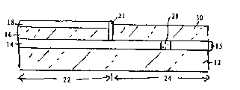
首先参照图1A-1G,示出了用于本发明来提供本发明半导体结构例如混合衬底以及所述混合衬底上的CMOS器件的基本工艺步骤。本发明的工艺开始于提供图1A所示的衬底10。如所示,衬底10包含上部半导体材料16、埋置的绝缘层14、以及下部半导体层12。表面介质18也可以被置于上部半导体材料16的顶部上。Referring first to FIGS. 1A-1G , there are shown the basic process steps used in the present invention to provide the inventive semiconductor structures, eg, hybrid substrates, and CMOS devices on said hybrid substrates. The process of the present invention begins by providing a
衬底10的表面介质18包含氧化物、氮化物、氮氧化物、或它们的多层,例如执行层转移工艺之前存在于初始晶片之一中的氮化物/氧化物叠层,或可以在层转移工艺之后被形成在上部半导体材料16的顶部上。当表面介质18在层转移工艺之后被形成在半导体材料16上时,可以采用热工艺(例如氧化、氮化、或氮氧化)或常规的淀积工艺(例如化学气相淀积(CVD)、等离子体增强化学气相淀积(PECVD)、化学溶液淀积、或蒸发)。尽管表面介质层18的起源如此,但表面介质层18的厚度典型约为3-500nm。The surface dielectric 18 of the
衬底10的上部半导体材料16由任何半导体材料组成,例如包括Si、SiC、SiGe、SiGeC、Ge合金、GaAs、InAs、InP、以及其它的III/V或II/VI族化合物半导体。上部半导体材料16还可以包含预先形成的SOI衬底或诸如Si/SiGe之类的层状半导体的SOI层。上部半导体材料16的特征还在于具有优选为(110)的第一晶向。虽然(110)晶向是优选的,但第一半导体层16可以具有(111)或(100)晶向。要指出的是,上部半导体材料16形成了本发明混合衬底的第一半导体材料。The
依赖于用来形成衬底10的初始晶片,上部半导体材料16的厚度可以变化。但典型地说,上部半导体材料16的厚度约为5-500nm,以约为5-100nm的厚度更为优选。Depending on the initial wafer used to form
位于上部半导体材料16与下部半导体材料12之间的绝缘层14(或埋置的绝缘层14)具有依赖于用来产生衬底10的初始晶片的可变厚度。但典型地说,绝缘层14的厚度约为1-500nm,以约为5-100nm的厚度更为典型。绝缘层14是在执行层转移工艺之前形成在一个或二个晶片上的氧化物或其它相似的绝缘体材料。The insulating layer 14 (or buried insulating layer 14 ) between the upper
下部半导体材料12由任何半导体材料组成,可以与上部半导体材料16相同或不同。于是,下部半导体材料12可以包括例如Si、SiC、SiGe、SiGeC、Ge合金、GaAs、InAs、InP、以及其它的III/V或II/VI族化合物半导体。下部半导体材料12还可以包含预先形成的SOI衬底或诸如Si/SiGe之类的层状半导体的SOI层。下部半导体材料12的特征还在于具有不同于第一晶向的第二晶向。注意,下部半导体材料12的晶向将决定随后要用外延方法再生长在材料12的暴露部分上的第二半导体材料的晶向。由于上部半导体材料16优选是(110)表面,故下部半导体材料12的晶向优选是(100)。虽然(100)晶向是优选的,但下部半导体材料12可以具有(111)或(100)晶体结构。Lower
依赖于用来形成衬底10的初始晶片,下部半导体材料12的厚度可以变化。但典型地说,下部半导体材料12的厚度约为5-200nm,以约为5-100nm的厚度更为典型。Depending on the initial wafer used to form
用层转移工艺来形成图1A所示的衬底10,其中采用了至少二个晶片的键合。用来制作衬底10的二个晶片可以包括二个SOI晶片,其中一个晶片包括衬底10的上部半导体材料16,而另一个晶片包括衬底10的下部半导体材料12;一个SOI晶片和一个体半导体晶片;其上都包含绝缘层14的二个体半导体晶片;或一个SOI晶片和一个包括能够在层转移工艺过程中用来分裂至少一个晶片一部分的诸如氢注入区的离子注入区的体晶片。The
借助于首先使二个晶片彼此紧密接触,可选地将外力施加到接触的晶片,然后在能够将二个晶片键合到一起的条件下对二个接触的晶片进行加热,来达到层转移。可以在存在或不存在外力的情况下执行加热步骤。典型地在惰性气氛中于大约200-1050℃的温度下,执行大约2-20小时的加热步骤。更典型的是,在大约200-400℃的温度下来执行键合。此处还尝试了其它也能够键合二个晶片的键合温度和时间。在本发明中,术语“惰性气氛”被用来表示其中使用诸如He、Ar、N2、Xe、Kr、或它们的混合物之类的惰性气体的气氛。键合工艺中使用的优选气氛是N2。Layer transfer is achieved by first bringing the two wafers into intimate contact with each other, optionally applying an external force to the contacting wafers, and then heating the two contacting wafers under conditions capable of bonding the two wafers together. The heating step can be performed with or without external force. The heating step is typically performed at a temperature of about 200-1050° C. for about 2-20 hours in an inert atmosphere. More typically, bonding is performed at a temperature of about 200-400°C. Other bonding temperatures and times that also bonded the two wafers were also tried here. In the present invention, the term "inert atmosphere" is used to mean an atmosphere in which an inert gas such as He, Ar,N2 , Xe, Kr, or a mixture thereof is used. A preferred atmosphere used in the bonding process isN2 .
在使用二个SOI晶片的实施方案中,在键合之后,可以用诸如化学机械抛光(CMP)或研磨以及蚀刻之类的整平工艺来清除至少一个SOI晶片的某些材料层。当达及表面介质层18时,整平工艺就停止。于是,表面介质层18在本发明中能够用作蚀刻停止层。In embodiments using two SOI wafers, after bonding, some material layers of at least one SOI wafer may be removed with a planarization process such as chemical mechanical polishing (CMP) or grinding and etching. When the
在其中一个晶片包括离子注入区的实施方案中,离子注入区在键合过程中形成了多孔区,这使得离子注入区上的一部分晶片从衬底10剥离,如图1A所示。此注入区典型地由利用本技术领域熟练人员熟知的离子注入条件注入到晶片表面中的氢离子组成。在此实施方案中,典型地采用比上述温度更低的键合温度。In an embodiment where one of the wafers includes an ion-implanted region, the ion-implanted region forms a porous region during the bonding process, which causes a portion of the wafer above the ion-implanted region to be lifted from the
然后,在图1A的衬底10预定部分上形成掩模20,以便保护部分衬底10,同时留下衬底10的其它部分不被保护。被保护的衬底10部分确定了第一半导体区22,而未被保护的衬底10部分确定了第二半导体区24。Then, a
在一个实施方案中,借助于将光抗蚀剂掩模涂敷到衬底10的整个表面,掩模20被形成在表面介质层18的预定部分上。在涂敷光抗蚀剂掩模之后,用光刻方法对掩模进行图形化,此光刻方法包括将光抗蚀剂暴露于辐射图形以及用抗蚀剂显影剂显影图形。在另一实施方案中,掩模20是用光刻和蚀刻方法形成和图形化的氮化物或氮氧化物层。在确定第二半导体区24之后,可以清除氮化物或氮氧化物掩模20。例如图1B示出了得到的包括形成在衬底10预定部分上的掩模20的结构;各种半导体区被标注为22和24。In one embodiment,
在对衬底10提供确定各种半导体区的掩模20之后,对结构进行第一蚀刻步骤,包括在第二半导体区24内确定有源区RX的第一掩模层(未示出)。此第一蚀刻步骤清除了表面介质层18的未被保护部分以及上部半导体层16的下方部分,停止于绝缘层14的顶部。可以用单个蚀刻工艺来执行此蚀刻步骤,或可以采用多个蚀刻步骤。本发明此时所用的蚀刻,可以包括诸如反应离子刻蚀、离子束蚀刻、等离子体蚀刻、或激光蚀刻之类的干法蚀刻,其中采用化学蚀刻剂的湿法蚀刻,或它们的任何组合。在本发明的优选实施方案中,反应离子刻蚀(RIE)被用来选择性地清除表面介质层18和上部半导体材料16的未被保护部分,停止于第二半导体区24中的绝缘层14的表面上。After providing the
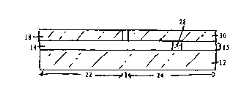
在第二半导体区24内确定有源区RX之后,第二掩蔽层(未示出)被用来在绝缘层14的暴露部分中确定至少一个外延窗口26,然后,第二蚀刻工艺被用来清除暴露的埋置绝缘层14,在第二半导体区24内提供不连续的埋置绝缘层15;此不连续性由窗口26来提供。注意,用来在第二半导体区24中确定窗口26的掩模层小于有源区RX。第二蚀刻工艺包括选择性地清除埋置绝缘层14暴露部分,停止于下部半导体材料12表面上的任何蚀刻技术。例如图1C示出了在已经执行第一和第二蚀刻工艺之后得到的结构。注意,被保护的第一半导体区22亦即表面介质层18和上部半导体材料16的侧壁,在此蚀刻步骤之后被暴露。如所示,层18和16的暴露侧壁与掩模20的最外边沿对准。还要注意的是,由于连续的埋置绝缘层14在本发明中未发生蚀刻,故连续的埋置绝缘层14存在于第一半导体区22中。After defining the active region RX in the
然后,利用常规的抗蚀剂剥离工艺,从图1C所示的结构清除掩模20,然后典型地但不总是在暴露的侧壁上形成衬里即隔垫21。用淀积和蚀刻方法来形成此可选的衬里即隔垫21。当提供衬里即隔垫21时,衬里即隔垫21由诸如氧化物之类的绝缘材料组成。The
接着,至少一个反掺杂区28和半导体材料30被形成为反掺杂区28位于各个窗口26内,而半导体材料30被形成在反掺杂区28上,将第二半导体区24的RX填充。根据本发明,除了掺杂(用离子注入或原位外延生长方法)发生在窗口26内以便在窗口中形成反掺杂区之外,区域28和30由相同的材料组成。于是,反掺杂区28在第二半导体区24内的埋置绝缘层中至少提供了一个裂口,但此区域保持类SOI。而且,反掺杂区在电学上将半导体材料30隔离于第二半导体区24中的下部半导体材料12。Next, at least one
在本发明中,反掺杂区28包括第一导电类型(P或N,优选为P)的上部掺杂区、不同于第一导电类型的第二导电类型(N或P,优选为N)的中部掺杂区、以及所述第一导电类型(P或N,优选为P)的下部掺杂区。In the present invention, the
在本发明的某些实施方案中,至少一个反掺杂区28具有这样一种掺杂分布,此掺杂分布为更好地控制SCE且消除额外的电容、泄漏、以及迁移率退化而设计。例如,反掺杂区28可以包含上部P掺杂区、中部N掺杂区、以及下部P掺杂区,其中,相对于相同导电类型的下部掺杂区,上部P掺杂区在靠近将包括器件沟道的半导体材料处,具有较高的掺杂剂浓度。In certain embodiments of the present invention, at least one
用外延随之以离子注入,或用原位外延生长工艺,来形成反掺杂区28。反掺杂区的掺杂量可以由本技术领域的熟练人员来选择。典型地说,用举例的方法,上部掺杂区是掺杂剂浓度约为每立方厘米5×10¹⁷-5×10¹⁹原子的P掺杂区,中部掺杂区是掺杂剂浓度约为每立方厘米5×10¹⁶-5×10¹⁸原子的N掺杂区,而下部掺杂区是掺杂剂浓度约为每立方厘米1×10¹⁶-5×10¹⁸原子的P掺杂区。The
根据本发明,半导体材料30以及反掺杂区28具有相同于下部半导体材料12的晶向。得到的结构被示于例如图1D中。According to the invention, the
半导体材料30(以及反掺杂区28)可以包含能够用选择性外延生长方法形成的任何含硅的半导体,例如Si、应变的Si、SiGe、SiC、SiGeC、或它们的组合。在某些优选实施方案中,半导体材料30由Si组成。在其它优选实施方案中,半导体材料30是位于驰豫SiGe合金层顶部上的应变硅层。在本发明中,半导体材料30可以被称为再生长的半导体材料,或简单地称为本发明混合衬底的第二半导体材料。Semiconductor material 30 (and counter-doped region 28 ) may comprise any silicon-containing semiconductor capable of being formed by selective epitaxial growth methods, such as Si, strained Si, SiGe, SiC, SiGeC, or combinations thereof. In certain preferred embodiments,
接着,对图1D所示的结构进行诸如化学机械抛光(CMP)或研磨之类的整平工艺,使半导体材料(亦即第二半导体材料)30的上表面与上部半导体材料(亦即第一半导体材料)16的上表面基本上齐平。注意,表面介质层18的先前被保护的部分在这一整平工艺中被清除。图1E示出了被整平的结构。可以增加一个可选的氧化步骤,以便改善半导体材料30的表面性质。Next, a leveling process such as chemical mechanical polishing (CMP) or grinding is performed on the structure shown in FIG. The upper surface of semiconductor material) 16 is substantially flush. Note that previously protected portions of the
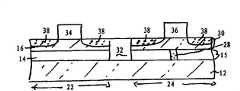
在提供了基本上平坦的表面之后,典型地形成诸如浅沟槽隔离区之类的隔离区32,以便将第一半导体区22隔离于第二半导体区24。用例如包括沟槽确定和蚀刻、用扩散势垒可选地对沟槽进行衬里、以及用诸如氧化物的沟槽介质填充沟槽的本技术领域熟练人员熟知的工艺步骤,来形成隔离区32。在沟槽填充之后,可以整平此结构,并可以执行可选的致密化工艺步骤,以便使沟槽介质致密。得到的包含隔离区32的混合结构被示于例如图1F。注意,衬里即隔垫21被隔离区32代替了。After providing the substantially planar surface,
图1G示出了在部分上部半导体层16上形成第一半导体器件34以及在再生长的半导体材料30上形成第二半导体器件36之后所形成的集成结构。尽管示出了在各个器件区中仅仅存在一个半导体器件,但本发明还尝试了在特定的器件区中形成多个各类型的器件。根据本发明,第一半导体器件可以是pFET或nFET,而第二半导体器件可以是nFET或pFET,但须第一半导体器件不同于第二半导体器件且特定的器件被制作在提供高性能器件的晶向上。用本技术领域熟练人员熟知的标准CMOS工艺步骤来制作这些pFET和nFET。各个FET包括栅介质、栅导体、位于栅导体顶部上的可选的硬掩模、位于至少栅导体侧壁上的隔垫、以及源/漏扩散区。此扩散区在图1G中被标注为38。注意,pFET被制作在晶向为(110)或(111)的半导体材料上,而nFET被制作在晶向为(100)或(111)的半导体表面上。FIG. 1G shows the resulting integrated structure after forming a
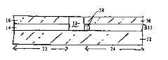
图2示出了能够用上述工艺制作的另一个混合衬底。在所示的实施方案中,反掺杂区28被形成到第二半导体区24中,使之位于得到的nFET的源区处或得到的pFET的漏区处。Figure 2 shows another hybrid substrate that can be fabricated with the above process. In the illustrated embodiment, a
图3示出了能够用上述工艺制作的另一个混合衬底。在所示图中,SOI、本体、以及赝式SOI能够被集成在一起,且存储器和/或模拟器件被制作在本体器件区中。注意,所示结构的右边部分与图1F所示的相同。在图3中,如上所述,相似的材料用相似的参考号表示。邻接第一半导体区22的左边部分包括:包含第三晶向的第三半导体材料16的第三半导体区50以及包含第四晶向的第四半导体材料30的第四半导体区52,其中,第三晶向不同于第四晶向,但相同于第一晶向,且所述第四晶向相同于第二晶向。注意,在图中,参考号16和30分别被用来表示第三和第四半导体材料。在此实施方案中,半导体材料各具有彼此共平面的上表面,且第三或第四区域之一包括连续的埋置绝缘层,而所述第三或第四区域中的所述另一个存在于具有所述第二晶向的半导体衬底上。Figure 3 shows another hybrid substrate that can be fabricated with the above process. In the diagram shown, SOI, bulk, and pseudo-SOI can be integrated together, and memory and/or analog devices are fabricated in the bulk device region. Note that the right part of the structure shown is the same as that shown in Figure 1F. In FIG. 3, like materials are denoted by like reference numerals as described above. The left part adjacent to the
虽然对于其优选实施方案已经具体地描述了本发明,但本技术领域熟练人员可以理解的是,可以作出形式和细节方面的上述和其它的改变而不偏离本发明的构思与范围。因此认为本发明不局限于所述的准确形式和细节,而是在所附权利要求的范围内。While the invention has been particularly described with respect to preferred embodiments thereof, it will be understood by those skilled in the art that the above and other changes in form and detail may be made without departing from the spirit and scope of the invention. It is therefore intended that the invention not be limited to the exact form and details described, but rather be within the scope of the appended claims.
Claims (29)
Translated fromChineseApplications Claiming Priority (2)
| Application Number | Priority Date | Filing Date | Title |
|---|---|---|---|
| US11/066,659 | 2005-02-25 | ||
| US11/066,659US7268377B2 (en) | 2005-02-25 | 2005-02-25 | Structure and method of fabricating a hybrid substrate for high-performance hybrid-orientation silicon-on-insulator CMOS devices |
Publications (2)
| Publication Number | Publication Date |
|---|---|
| CN1828908A CN1828908A (en) | 2006-09-06 |
| CN100411180Ctrue CN100411180C (en) | 2008-08-13 |
Family
ID=36932457
Family Applications (1)
| Application Number | Title | Priority Date | Filing Date |
|---|---|---|---|
| CNB2006100024675AExpired - Fee RelatedCN100411180C (en) | 2005-02-25 | 2006-01-26 | Semiconductor structure and method of manufacturing semiconductor structure |
Country Status (3)
| Country | Link |
|---|---|
| US (3) | US7268377B2 (en) |
| CN (1) | CN100411180C (en) |
| TW (1) | TWI353671B (en) |
Families Citing this family (25)
| Publication number | Priority date | Publication date | Assignee | Title |
|---|---|---|---|---|
| US7268377B2 (en)* | 2005-02-25 | 2007-09-11 | International Business Machines Corporation | Structure and method of fabricating a hybrid substrate for high-performance hybrid-orientation silicon-on-insulator CMOS devices |
| WO2006103491A1 (en)* | 2005-03-29 | 2006-10-05 | S.O.I.Tec Silicon On Insulator Technologies | Hybrid fully soi-type multilayer structure |
| US7432149B2 (en)* | 2005-06-23 | 2008-10-07 | Taiwan Semiconductor Manufacturing Company, Ltd. | CMOS on SOI substrates with hybrid crystal orientations |
| US7611937B2 (en)* | 2005-06-24 | 2009-11-03 | Taiwan Semiconductor Manufacturing Company, Ltd. | High performance transistors with hybrid crystal orientations |
| US7986029B2 (en)* | 2005-11-08 | 2011-07-26 | Taiwan Semiconductor Manufacturing Company, Ltd. | Dual SOI structure |
| US7531392B2 (en)* | 2006-02-27 | 2009-05-12 | International Business Machines Corporation | Multi-orientation semiconductor-on-insulator (SOI) substrate, and method of fabricating same |
| US7396407B2 (en)* | 2006-04-18 | 2008-07-08 | International Business Machines Corporation | Trench-edge-defect-free recrystallization by edge-angle-optimized solid phase epitaxy: method and applications to hybrid orientation substrates |
| US7776726B2 (en)* | 2006-05-04 | 2010-08-17 | Infineon Technologies Ag | Semiconductor devices and methods of manufacture thereof |
| US7808082B2 (en)* | 2006-11-14 | 2010-10-05 | International Business Machines Corporation | Structure and method for dual surface orientations for CMOS transistors |
| US7863653B2 (en)* | 2006-11-20 | 2011-01-04 | International Business Machines Corporation | Method of enhancing hole mobility |
| US20080169535A1 (en)* | 2007-01-12 | 2008-07-17 | International Business Machines Corporation | Sub-lithographic faceting for mosfet performance enhancement |
| US7728364B2 (en)* | 2007-01-19 | 2010-06-01 | International Business Machines Corporation | Enhanced mobility CMOS transistors with a V-shaped channel with self-alignment to shallow trench isolation |
| US20090200635A1 (en)* | 2008-02-12 | 2009-08-13 | Viktor Koldiaev | Integrated Circuit Having Electrical Isolation Regions, Mask Technology and Method of Manufacturing Same |
| US8211786B2 (en) | 2008-02-28 | 2012-07-03 | International Business Machines Corporation | CMOS structure including non-planar hybrid orientation substrate with planar gate electrodes and method for fabrication |
| US8053304B2 (en)* | 2009-02-24 | 2011-11-08 | Taiwan Semiconductor Manufacturing Company, Ltd. | Method of forming high-mobility devices including epitaxially growing a semiconductor layer on a dislocation-blocking layer in a recess formed in a semiconductor substrate |
| US8395216B2 (en) | 2009-10-16 | 2013-03-12 | Texas Instruments Incorporated | Method for using hybrid orientation technology (HOT) in conjunction with selective epitaxy to form semiconductor devices with regions of different electron and hole mobilities and related apparatus |
| US8698244B2 (en)* | 2009-11-30 | 2014-04-15 | International Business Machines Corporation | Silicon-on-insulator (SOI) structure configured for reduced harmonics, design structure and method |
| US8471340B2 (en) | 2009-11-30 | 2013-06-25 | International Business Machines Corporation | Silicon-on-insulator (SOI) structure configured for reduced harmonics and method of forming the structure |
| US9275911B2 (en) | 2012-10-12 | 2016-03-01 | Globalfoundries Inc. | Hybrid orientation fin field effect transistor and planar field effect transistor |
| KR102083495B1 (en) | 2013-01-07 | 2020-03-02 | 삼성전자 주식회사 | Complementary Metal Oxide Semiconductor device, optical apparatus comprising CMOS device and method of manufacturing the same |
| US9515068B1 (en) | 2013-08-29 | 2016-12-06 | Hrl Laboratories, Llc | Monolithic integration of GaN and InP components |
| US9490161B2 (en)* | 2014-04-29 | 2016-11-08 | International Business Machines Corporation | Channel SiGe devices with multiple threshold voltages on hybrid oriented substrates, and methods of manufacturing same |
| KR20160074210A (en)* | 2014-12-18 | 2016-06-28 | 에스케이하이닉스 주식회사 | Multi channel self refresh device |
| CN105206584B (en)* | 2015-08-28 | 2018-09-14 | 西安电子科技大学 | Heterogeneous channel trench gate CMOS integrated device and its preparation method |
| US11502106B2 (en)* | 2020-02-11 | 2022-11-15 | Globalfoundries U.S. Inc. | Multi-layered substrates of semiconductor devices |
Citations (3)
| Publication number | Priority date | Publication date | Assignee | Title |
|---|---|---|---|---|
| US5384473A (en)* | 1991-10-01 | 1995-01-24 | Kabushiki Kaisha Toshiba | Semiconductor body having element formation surfaces with different orientations |
| CN1389920A (en)* | 2001-05-31 | 2003-01-08 | 株式会社东芝 | Semiconductor device |
| US20040075141A1 (en)* | 2002-10-17 | 2004-04-22 | Renesas Technology Corp. | Semiconductor device and method of manufacturing same |
Family Cites Families (5)
| Publication number | Priority date | Publication date | Assignee | Title |
|---|---|---|---|---|
| JPS5662356A (en)* | 1979-10-26 | 1981-05-28 | Seiko Instr & Electronics Ltd | Logic integrated circuit device and its manufacturing method |
| US6902962B2 (en)* | 2003-04-04 | 2005-06-07 | Taiwan Semiconductor Manufacturing Company, Ltd. | Silicon-on-insulator chip with multiple crystal orientations |
| US7208815B2 (en)* | 2004-05-28 | 2007-04-24 | Taiwan Semiconductor Manufacturing Company, Ltd. | CMOS logic gate fabricated on hybrid crystal orientations and method of forming thereof |
| US7268377B2 (en)* | 2005-02-25 | 2007-09-11 | International Business Machines Corporation | Structure and method of fabricating a hybrid substrate for high-performance hybrid-orientation silicon-on-insulator CMOS devices |
| US6972478B1 (en)* | 2005-03-07 | 2005-12-06 | Advanced Micro Devices, Inc. | Integrated circuit and method for its manufacture |
- 2005
- 2005-02-25USUS11/066,659patent/US7268377B2/ennot_activeExpired - Fee Related
- 2006
- 2006-01-26CNCNB2006100024675Apatent/CN100411180C/ennot_activeExpired - Fee Related
- 2006-02-17TWTW095105329Apatent/TWI353671B/ennot_activeIP Right Cessation
- 2007
- 2007-07-30USUS11/830,489patent/US7425483B2/ennot_activeExpired - Fee Related
- 2008
- 2008-06-24USUS12/145,024patent/US7833854B2/ennot_activeExpired - Fee Related
Patent Citations (3)
| Publication number | Priority date | Publication date | Assignee | Title |
|---|---|---|---|---|
| US5384473A (en)* | 1991-10-01 | 1995-01-24 | Kabushiki Kaisha Toshiba | Semiconductor body having element formation surfaces with different orientations |
| CN1389920A (en)* | 2001-05-31 | 2003-01-08 | 株式会社东芝 | Semiconductor device |
| US20040075141A1 (en)* | 2002-10-17 | 2004-04-22 | Renesas Technology Corp. | Semiconductor device and method of manufacturing same |
Also Published As
| Publication number | Publication date |
|---|---|
| US7833854B2 (en) | 2010-11-16 |
| CN1828908A (en) | 2006-09-06 |
| US7425483B2 (en) | 2008-09-16 |
| US20080261354A1 (en) | 2008-10-23 |
| TW200640008A (en) | 2006-11-16 |
| US20060194421A1 (en) | 2006-08-31 |
| US20070269945A1 (en) | 2007-11-22 |
| US7268377B2 (en) | 2007-09-11 |
| TWI353671B (en) | 2011-12-01 |
Similar Documents
| Publication | Publication Date | Title |
|---|---|---|
| CN100411180C (en) | Semiconductor structure and method of manufacturing semiconductor structure | |
| US7364958B2 (en) | CMOS on hybrid substrate with different crystal orientations using silicon-to-silicon direct wafer bonding | |
| US7915100B2 (en) | Hybrid orientation CMOS with partial insulation process | |
| US8097516B2 (en) | Dual trench isolation for CMOS with hybrid orientations | |
| US6995456B2 (en) | High-performance CMOS SOI devices on hybrid crystal-oriented substrates | |
| US6998684B2 (en) | High mobility plane CMOS SOI | |
| US7605429B2 (en) | Hybrid crystal orientation CMOS structure for adaptive well biasing and for power and performance enhancement | |
| CN100461430C (en) | Semiconductor structures and methods of forming them | |
| US7687365B2 (en) | CMOS structure for body ties in ultra-thin SOI (UTSOI) substrates | |
| US7834425B2 (en) | Hybrid orientation SOI substrates, and method for forming the same | |
| US20080224255A1 (en) | Subground rule sti fill for hot structure | |
| US7479410B2 (en) | Hybrid-orientation technology buried n-well design | |
| CN100361302C (en) | Hybrid substrates, integrated semiconductor structures, and methods of making them |
Legal Events
| Date | Code | Title | Description |
|---|---|---|---|
| C06 | Publication | ||
| PB01 | Publication | ||
| C10 | Entry into substantive examination | ||
| SE01 | Entry into force of request for substantive examination | ||
| C14 | Grant of patent or utility model | ||
| GR01 | Patent grant | ||
| C17 | Cessation of patent right | ||
| CF01 | Termination of patent right due to non-payment of annual fee | Granted publication date:20080813 Termination date:20120126 |