CN100410985C - Image display unit and method of correcting brightness in image display unit - Google Patents
Image display unit and method of correcting brightness in image display unitDownload PDFInfo
- Publication number
- CN100410985C CN100410985CCNB2005101069221ACN200510106922ACN100410985CCN 100410985 CCN100410985 CCN 100410985CCN B2005101069221 ACNB2005101069221 ACN B2005101069221ACN 200510106922 ACN200510106922 ACN 200510106922ACN 100410985 CCN100410985 CCN 100410985C
- Authority
- CN
- China
- Prior art keywords
- correction data
- unbalance
- pixel
- display
- section
- Prior art date
- Legal status (The legal status is an assumption and is not a legal conclusion. Google has not performed a legal analysis and makes no representation as to the accuracy of the status listed.)
- Expired - Fee Related
Links
Images


Landscapes
- Control Of Indicators Other Than Cathode Ray Tubes (AREA)
Abstract
Description
Translated fromChinese本发明包含与2004年9月22日向日本专利局提交的日本专利申请JP2004-274794以及2005年5月23日向日本专利局提交的日本专利申请JP2005-149280相关的主题,这里通过引用而合并其全部内容。The present invention contains subject matter related to Japanese Patent Application JP2004-274794 filed in Japan Patent Office on September 22, 2004 and Japanese Patent Application JP2005-149280 filed in Japan Patent Office on May 23, 2005, which are hereby incorporated by reference in their entirety content.
技术领域technical field
本发明涉及一种包含多个像素并且逐像素地控制显示亮度电平的显示单元,例如适合于FED(场致发射显示器)、EL(场致发光)显示器、液晶显示器单元等等的图像显示单元,以及一种校正图像显示单元中的亮度的方法。The present invention relates to a display unit comprising a plurality of pixels and controlling the display brightness level on a pixel-by-pixel basis, such as an image display unit suitable for FED (Field Emission Display), EL (Electroluminescence) display, liquid crystal display unit, etc. , and a method of correcting brightness in an image display unit.
背景技术Background technique
近年来,显示器单元已经变得越来越薄,越来越平。作为一种用于显示单元的平板显示部件(平板显示器,此后简称为显示器),已经开发了例如利用场致发射阴极的显示器。公知FED是一种利用场致发射阴极的显示器。FED具有许多优点:FED可以提高灰度,同时保证了观看角度,并且图像质量良好,生产效率高,响应速度高,FED可以在极低温环境下运行,亮度高,并且功效高。另外,与所谓有源矩阵液晶显示器的制造工艺相比,FED的制造工艺较简单,并且FED的制造成本有望比有源矩阵液晶显示器的制造成本低至少40%到60%。In recent years, display units have become thinner and flatter. As a flat panel display part (flat panel display, hereinafter simply referred to as a display) for a display unit, for example, a display using a field emission cathode has been developed. A known FED is a display utilizing a field emission cathode. FED has many advantages: FED can improve the gray level while ensuring the viewing angle, and the image quality is good, the production efficiency is high, the response speed is high, the FED can operate in an extremely low temperature environment, the brightness is high, and the power efficiency is high. In addition, the manufacturing process of the FED is simpler compared to that of the so-called active matrix liquid crystal display, and the manufacturing cost of the FED is expected to be at least 40% to 60% lower than that of the active matrix liquid crystal display.
以下将描述FED的基本结构与操作。FED是这样一种显示设备,其中通过利用场致电子发射特性,从场致发射阴极发射电子,并且对电子施加加速电场以使电子加速,然后当电子击中覆盖磷的阳极电极时获得光发射。The basic structure and operation of the FED will be described below. FED is a display device in which electrons are emitted from a field emission cathode by utilizing field electron emission characteristics, and an accelerating electric field is applied to the electrons to accelerate the electrons, and then light emission is obtained when the electrons hit a phosphor-covered anode electrode .
场致发射阴极包括例如锥形阴极设备(冷阴极设备)以及电连接到阴极设备基座的阴极电极。另外,在面对阴极电极的一侧,安置栅极电极,它们之间有阴极设备。当在彼此相对的阴极电极与栅极电极之间施加电压Vgc时,从阴极设备发射电子。在面对场致发射阴极与栅极电极的一侧,安置阳极电极,作为加速电极。当向阳极电极施加高压HV时,从阴极设备发射的电子被加速,击中施加到阳极电极上的磷,由此发射光。The field emission cathode comprises, for example, a tapered cathode device (cold cathode device) and a cathode electrode electrically connected to the base of the cathode device. In addition, on the side facing the cathode electrode, a grid electrode is arranged with the cathode device in between. When a voltage Vgc is applied between the cathode electrode and the gate electrode facing each other, electrons are emitted from the cathode device. On the side facing the field emission cathode and the grid electrode, an anode electrode is arranged as an accelerating electrode. When a high voltage HV is applied to the anode electrode, electrons emitted from the cathode device are accelerated, hit the phosphor applied to the anode electrode, thereby emitting light.
一般地,在FED中,栅极电极连接到行方向的(Row)线以及列方向的(Column)线以实现矩阵布线,并且在线的每个交叉点上安排阴极设备,从而以矩阵形式形成像素。从列方向线一侧输入调制信号,从行方向线一侧依次施加扫描信号以进行扫描。当作为扫描信号的行线选择电压Vrow从行方向施加到栅极电极、并且作为调制信号的列线驱动电压Vcol从列方向施加到阴极电极时,在栅极电极与阴极电极之间产生表示为Vgc的电压差,并且通过由电压Vgc生成的电场而从阴极设备发射电子。此时,当向阳极电极施加高压HV时,在以下条件下,电子被吸引到阳极电极,由此阳极电流Ia沿从阳极电极到阴极电极的方向流动。Generally, in a FED, gate electrodes are connected to row-direction (Row) lines and column-direction (Column) lines to realize matrix wiring, and cathode devices are arranged at each intersection of the lines to form pixels in a matrix . The modulating signal is input from the line side in the column direction, and the scanning signal is sequentially applied from the line side in the row direction to perform scanning. When the row line selection voltage Vrow as a scan signal is applied to the gate electrode from the row direction, and the column line drive voltage Vcol as a modulation signal is applied to the cathode electrode from the column direction, a voltage expressed as Vgc voltage difference, and electrons are emitted from the cathode device by the electric field generated by the voltage Vgc. At this time, when a high voltage HV is applied to the anode electrode, electrons are attracted to the anode electrode under the following conditions, whereby the anode current Ia flows in a direction from the anode electrode to the cathode electrode.
HV>Vrow............(1)HV>Vrow......(1)
此时,当磷被施加到阳极电极时,磷借助电子能量发射光。At this time, when phosphorus is applied to the anode electrode, the phosphorus emits light by electron energy.
依赖于电压Vgc的幅度,电子发射量发生变化,由此阳极电流Ia发生变化。在这种情况下,磷的光发射量(即光发射亮度L)具有以下关系。Depending on the magnitude of the voltage Vgc, the amount of electron emission varies, and thus the anode current Ia varies. In this case, the light emission amount of phosphor (ie, light emission luminance L) has the following relationship.
L∝Ia............(2)L∝Ia..........(2)
因此,当改变电压Vgc时,可以改变光发射亮度L。换言之,当通过电压Vgc的幅度控制电子发射量时,就可以获得所希望的光发射。由此,当根据要显示的信号调制电压Vgc时,就可以实现亮度调制。Therefore, when the voltage Vgc is changed, the light emission luminance L can be changed. In other words, when the amount of electron emission is controlled by the magnitude of the voltage Vgc, desired light emission can be obtained. Thus, when the voltage Vgc is modulated according to the signal to be displayed, brightness modulation can be realized.
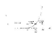
图1示出了阴极设备中电子发射特性(电流-电压特性(IV特性))的例子。横轴表示电压Vgc,纵轴表示电流Ic。如图1所示,在阴极设备中,虽然有小电流从门限Vo开始流动,但是在截止电压Von(例如20V)或更小电压上,没有发射对光发射有贡献的电子,并且当施加超过截止电压Von的电压作为电压Vgc时,发射电子生成对光发射有贡献的电流。FIG. 1 shows an example of electron emission characteristics (current-voltage characteristics (IV characteristics)) in a cathode device. The horizontal axis represents the voltage Vgc, and the vertical axis represents the current Ic. As shown in FIG. 1, in the cathode device, although a small current flows from the threshold Vo, no electrons contributing to light emission are emitted at the cut-off voltage Von (for example, 20 V) or less, and when applied more than When the voltage of the cut-off voltage Von is the voltage Vgc, electrons are emitted to generate a current that contributes to light emission.
作为行线选择电压Vrow,例如在选择时施加35V电压,或者在未选择时施加0V电压。另一方面,作为列线驱动电压Vcol,例如根据输入图像信号电平而施加0至15V的调制信号。As the row line selection voltage Vrow, for example, a voltage of 35V is applied when selecting, or a voltage of 0V is applied when not selecting. On the other hand, as the column line driving voltage Vcol, for example, a modulation signal of 0 to 15V is applied in accordance with the input image signal level.
在这种情况下,当行线选择电压Vrow处于选择状态,即施加35V电压,并且列线驱动电压Vcol为0V时,栅极与阴极之间的电压差Vgc为35V,使得从阴极设备发射的电子量增加,并且磷中所发射的光具有高亮度。类似地,当行线选择电压Vrow处于选择状态,即施加35V,并且列线驱动电压Vcol为15V时,栅极与阴极之间的电压差Vgc为20V。然而,因为发射的电子具有图1所示的发射特性,所以当电压差Vgc为20V时,没有发射对光发射有贡献的充足的电子。因此,不发生光发射。In this case, when the row line selection voltage Vrow is in the selected state, that is, a voltage of 35V is applied, and the column line driving voltage Vcol is 0V, the voltage difference Vgc between the gate and the cathode is 35V, so that the electrons emitted from the cathode device The amount increases, and the light emitted from the phosphor has high brightness. Similarly, when the row line selection voltage Vrow is in the selected state, that is, 35V is applied, and the column line driving voltage Vcol is 15V, the voltage difference Vgc between the gate and the cathode is 20V. However, since the emitted electrons have the emission characteristics shown in FIG. 1, when the voltage difference Vgc is 20V, sufficient electrons to contribute to light emission are not emitted. Therefore, light emission does not occur.
如上所述,当使行线选择电压Vrow进入选择状态,并且根据输入图像信号电平而将列线驱动电压Vcol控制在0V至15V的范围内时,就可以显示所希望的亮度。As mentioned above, when the row line selection voltage Vrow is put into the selected state, and the column line driving voltage Vcol is controlled in the range of 0V to 15V according to the input image signal level, desired brightness can be displayed.
在连续显示面板、同时通过向栅极电极施加行线选择电压Vrow而逐行依次驱动(扫描)阴极设备阵列的情况下,同时向阴极电极组施加用于图像的一条线的调制信号(列线驱动电压Vcol),由此控制照射到磷的电子束量,以逐线显示图像。In the case of a continuous display panel while sequentially driving (scanning) the array of cathode devices row by row by applying a row line selection voltage Vrow to the gate electrodes, simultaneously applying a modulation signal for one line of the image (column line) to the cathode electrode group driving voltage Vcol), thereby controlling the amount of electron beams irradiated to the phosphor to display an image line by line.
在FED中,已知潜在地存在以下问题。In FED, the following problems are known to potentially exist.
(i)即使施加相同的电压Vgc,由于阴极设备或者布线的制造工艺变化,来自每个阴极设备的电子发射量也不相同。换言之,即使以相同的信号电平驱动所有像素,每个显示像素的亮度也不相同(即,每个像素的Vgc-亮度特性(γ特性)不会完全相同)。在这种情况下,制造工艺变化具有某些模式,因此在屏幕上有暗淡区域以及明亮区域,其可以被看做亮度失衡。另外,颜色之间的亮度失衡可以被看做颜色失衡。(i) Even if the same voltage Vgc is applied, the amount of electron emission from each cathode device varies due to variations in the manufacturing process of the cathode device or wiring. In other words, even if all pixels are driven at the same signal level, the luminance of each display pixel is not the same (ie, the Vgc-luminance characteristic (γ characteristic) of each pixel is not exactly the same). In this case, the manufacturing process variation has certain patterns, so there are dark areas as well as bright areas on the screen, which can be seen as a brightness imbalance. Additionally, an imbalance of lightness between colors can be seen as a color imbalance.
(ii)由于布线负载使得电压Vgc随屏幕位置而不同。(ii) The voltage Vgc differs depending on the screen position due to the wiring load.
FED具有矩阵布线结构,因此存在根据像素之间线长度的布线电阻。另外,行线与列线在像素部分相互交叉,因此生成了根据像素部分面积的布线电容(寄生电容)。该布线电阻与布线电容为布线负载。与驱动器的距离越大,由布线负载造成的电压降变得越大,并且靠近与远离驱动器之间存在电压差,因此即使从驱动器施加相同的电压,所施加的电压Vgc在每个像素中也不会相同,由此不会获得均匀的光发射。因此,会发生遮蔽(shading)现象,即靠近驱动器的光较亮,而与驱动器的距离越大,则光越暗。The FED has a matrix wiring structure, so there is wiring resistance according to the length of lines between pixels. In addition, row lines and column lines intersect with each other at the pixel portion, so wiring capacitance (parasitic capacitance) depending on the area of the pixel portion is generated. The wiring resistance and wiring capacitance are wiring loads. The greater the distance from the driver, the greater the voltage drop caused by the wiring load becomes, and there is a voltage difference between being close to and being far from the driver, so even if the same voltage is applied from the driver, the applied voltage Vgc is different in each pixel will not be the same, thus no uniform light emission will be obtained. Therefore, shading occurs, that is, the light near the driver is brighter, and the greater the distance from the driver, the darker the light.
这些是关于图像显示均匀性的基本问题。接着将描述相关技术中用来解决均匀性问题的校正系统的例子。在该校正系统中,预先准备好校正数据,并且向原始信号添加或从原始信号中减去该校正数据,以校正原始信号,由此提高均匀性。These are fundamental questions about image display uniformity. Next, an example of a correction system used to solve the uniformity problem in the related art will be described. In this correction system, correction data is prepared in advance, and is added to or subtracted from an original signal to correct the original signal, thereby improving uniformity.
更具体地讲,首先,如图2A所示,显示单元41中的有效屏幕42实际上被分割为间距大于实际像素间距的网格,并且在每个输入信号电平上测量被分割的格栅点43中的亮度。因为数据量较大,所以不对可以在显示单元41中显示的所有信号电平进行采样,而只对有代表性的信号电平进行采样,并然后在每个采样的信号电平上测量亮度。然后,根据测量数据,计算在每个采样的输入信号电平上每个格栅点43中的校正数据,并且将其存储在存储器中作为查找表。More specifically, first, as shown in FIG. 2A , the
在图2B中,在概念上将具有每个采样的输入信号电平上每个格栅点43中的校正数据44显示为三维像素空间。图2B所示的三维像素空间参数包括沿水平方向和垂直方向的像素位置以及信号电平。如图2A与2B所示,通过一次测量而测量输入信号电平n上每个格栅点43中的亮度,并且计算对于输入信号电平n上每个格栅点43的校正数据44。当在每个输入信号电平上进行这一处理时,计算在每个输入信号电平上每个格栅点43的校正数据44。In Fig. 2B, the
在这种情况下,必须具有(屏幕垂直方向上的格栅点个数×屏幕水平方向上的格栅点个数×输入信号电平样本个数)项数据,作为查找表形式的校正数据44。然后,通过基于存储在查找表中的每个格栅点43的校正数据44进行内插,而形成对于所有信号电平上所有像素的校正数据。In this case, it is necessary to have (the number of grid points in the vertical direction of the screen×the number of grid points in the horizontal direction of the screen×the number of samples of the input signal level) item data as the
图3以三维方式示出了借助内插计算校正数据的概念。在该图所示的三维像素空间中,根据围绕内插点45的8个格栅点43的校正数据,而计算内插点45的校正数据。内插点45的校正数据的值是根据与这8个格栅点43的每一个的距离的值。借助内插计算数据的方法包括线性内插。Figure 3 shows in three dimensions the concept of calculating correction data by means of interpolation. In the three-dimensional pixel space shown in the figure, the correction data of the
图4A与4B示出了借助线性内插计算校正数据的概念。图4A示出了垂直方向的线性内插,而图4B示出了水平方向的线性内插。在图4A中,当目标内插点45的位置为L3时,通过对于垂直方向上邻近点L1与L2中格栅点43的校正数据的值、以及从点L1与L2至点L3的距离a与b,而确定对于目标内插点45的校正数据。更具体地讲,对于目标内插点45的校正数据通过下列公式表示。在该公式中,L1、L2和L3表示数据值。4A and 4B illustrate the concept of calculating correction data by means of linear interpolation. FIG. 4A shows linear interpolation in the vertical direction, and FIG. 4B shows linear interpolation in the horizontal direction. In FIG. 4A, when the position of the
L3=(bL1+aL2)/(a+b)L3=(bL1+aL2)/(a+b)
类似地,在图4B中,当目标内插点45的位置为L13时,通过对于水平方向上邻近点L11与L12中的校正数据的值、以及从点L11与L12到点L13的距离a与b,而确定对于内插点45的校正数据。更具体地讲,对于目标内插点45的校正数据通过下列公式表示。在该公式中,L11、L12和L13表示数据值。点L11与L12中的数据值可以通过上述垂直方向上的线性内插确定。Similarly, in FIG. 4B, when the position of the
L13=(bL11+aL12)/(a+b)L13=(bL11+aL12)/(a+b)
由此,当将垂直方向上的线性内插与水平方向上的线性内插结合时,就可以确定任何位置中的数据值。通过与图4A和4B相同的计算,可以确定被采样的信号电平之间的内插,尽管没有显示。Thus, when linear interpolation in the vertical direction is combined with linear interpolation in the horizontal direction, data values in any position can be determined. Interpolation between sampled signal levels can be determined by the same calculations as in Figures 4A and 4B, although not shown.
在日本未审专利申请公开号2000-122598中描述了一种通过利用校正数据来提高亮度均衡性的技术。在该文献中,在包含多个光发射设备的显示单元中,通过参考对应于光发射设备的校正值表而校正光发射命令值,并且根据校正后的光发射命令值而控制驱动部分。校正值表存储对于每个光发射设备的校正值数据或者对于显示器部分的每个小区域的校正值数据。A technique for improving luminance uniformity by using correction data is described in Japanese Unexamined Patent Application Publication No. 2000-122598. In this document, in a display unit including a plurality of light emitting devices, a light emission command value is corrected by referring to a correction value table corresponding to the light emitting devices, and a driving section is controlled according to the corrected light emission command value. The correction value table stores correction value data for each light emitting device or correction value data for each small area of the display portion.
发明内容Contents of the invention
以下将描述通过上述相关技术中的校正系统来校正“失衡”的能力。图5示出对于输入信号电平上校正数据计算的格栅点的排列。在有效屏幕190中,不管是否存在失衡,都以固定间距排列格栅点191。因此,如图所示,当存在其中在相对较大的面积内出现失衡的A区域192以及其中在相对较小的面积内出现失衡的B区域193时,存在以下可能性:在A区域192中存在格栅点191,而在B区域193中不存在格栅点191。在存在格栅点191的情况下,如在A区域192中的情况,可以获得对应于失衡的校正数据,从而可以容易地校正失衡。然而,在不存在格栅点191的情况下,如在B区域193中的情况,不能获得对应于失衡的校正数据,从而不能校正失衡。因此,在失衡区域大于当设置格栅点191时的屏幕分割区域的情况下,校正能力较高,而当失衡区域较小时,校正能力较低。换言之,失衡越精细(其中出现失衡的面积越小),校正能力变得越低。在日本未审专利申请公开号2000-122598中,在存储对于显示部分的每个小面积的校正值数据的情况下,会出现相同的问题。The ability to correct "imbalance" by the correction system in the related art described above will be described below. Fig. 5 shows the arrangement of grid points calculated for the correction data at the input signal level. In the
为了校正较精细的失衡,如图6所示,必须通过减少屏幕分割区域的尺寸,而增加格栅点的数目,并且减少格栅点之间的间距。换言之,除图5所示的格栅点191之外,还必须增加格栅点194,并且必须增加校正数据。在图5所示的例子中,有48个格栅点191,而在图6中,增加了格栅点194,因此共有165个格栅点。由此,在具有精细失衡的B区域193中存在格栅点,从而可以获得校正数据,并且可以校正失衡。极端的方法是将分割区域的尺寸降低到一个像素的尺寸,并且在所有像素中设置格栅点;然而,如果这样做的话,则必须将对于所有像素的校正数据存储为查找表,由此极大的增加了必须的存储量。该极端的方法不实用,因为存储容量太大。在日本未审专利申请公开号2000-122598中,在存储对于每个光发射设备的校正值数据的情况下,会出现相同的问题。因此,人们希望有一种技术来改进校正能力,同时最小化存储在查找表中的校正数据量。In order to correct finer imbalances, as shown in FIG. 6, it is necessary to increase the number of grid points and decrease the spacing between grid points by reducing the size of the screen division area. In other words, grid points 194 must be added in addition to
鉴于上述,人们希望提供一种图像显示单元,其与相关技术相比,能够提高均匀性校正的能力,同时能够通过最小化预先准备的校正数据来减少存储量,以及一种校正图像显示单元中的亮度的方法。In view of the above, it is desired to provide an image display unit capable of improving the uniformity correction capability as compared with the related art, and at the same time reducing the amount of memory by minimizing correction data prepared in advance, and a correction image display unit in which method of brightness.
根据本发明的实施方式,提供了一种包括多个像素并且逐像素地控制显示亮度电平的图像显示单元,该图像显示单元包括:存储部件,用于存储用来校正像素之间显示失衡的对于设置在有效屏幕中的代表性像素点的校正数据;内插部件,用来通过参照存储在存储部件中的校正数据,借助内插计算对于除代表性像素点之外的像素的校正数据;以及信号处理部件,用来根据存储在存储部件中的校正数据以及通过内插所计算的校正数据,而对输入信号进行校正处理,使得相同输入信号电平上的显示亮度在各像素之间变得相同。在该图像显示单元中,代表性像素点的排列根据在进行校正处理之前测量的显示失衡而设置,使得在有效屏幕中的显示失衡相对较精细的像素区域内以比显示失衡粗糙的像素区域更高的密度排列代表性像素点,并且与显示失衡粗糙的像素区域相比,根据所测量的显示失衡而将存储在存储部件中的校正数据更多地分配到显示失衡相对较精细的像素区域。According to an embodiment of the present invention, there is provided an image display unit including a plurality of pixels and controlling a display brightness level on a pixel-by-pixel basis, the image display unit including: a storage unit for storing Correction data for representative pixel points set in the effective screen; interpolation means for calculating correction data for pixels other than the representative pixel points by means of interpolation by referring to the correction data stored in the storage part; and a signal processing section for correcting the input signal based on the correction data stored in the storage section and the correction data calculated by interpolation so that the display luminance at the same input signal level varies between pixels got the same. In this image display unit, the arrangement of representative pixel points is set according to the display imbalance measured before performing the correction process so that in the effective screen, the display imbalance is relatively finer in the pixel area than the display imbalance is rough in the pixel area. The representative pixel dots are arranged at a high density, and the correction data stored in the storage section based on the measured display imbalance is distributed more to the pixel area where the display imbalance is relatively fine than to the pixel area where the display imbalance is coarse.
根据本发明的实施方式,提供了一种校正图像显示单元中的亮度的方法,该图像显示单元包括多个像素、并且逐像素地控制显示亮度电平,该方法包含以下步骤:存储用来校正像素之间显示失衡的对于设置在有效屏幕中的代表性像素点的校正数据;通过参照所存储的校正数据,借助内插计算对于除代表性像素点之外的像素的校正数据;以及根据所存储的校正数据以及通过内插所计算的校正数据,而对输入信号进行校正处理,使得相同输入信号电平上的显示亮度在各像素之间变得相同。在该方法中,代表性像素点的排列根据在进行校正处理之前测量的显示失衡而设置,使得在有效屏幕中的显示失衡相对较精细的像素区域内以比显示失衡粗糙的像素区域更高的密度排列代表性像素点,并且与显示失衡粗糙的像素区域相比,根据所测量的显示失衡而将所存储的校正数据更多地分配到显示失衡相对较精细的像素区域。According to an embodiment of the present invention, there is provided a method of correcting brightness in an image display unit comprising a plurality of pixels and controlling the display brightness level pixel by pixel, the method comprising the following steps: storing Correction data for representative pixel points set in the effective screen showing an imbalance between pixels; calculating correction data for pixels other than the representative pixel points by interpolation by referring to the stored correction data; and The stored correction data and the correction data calculated by interpolation perform correction processing on the input signal so that the display luminance at the same input signal level becomes the same among the pixels. In this method, the arrangement of representative pixel points is set according to the display imbalance measured before performing the correction process so that in the pixel area where the display imbalance is relatively fine in the effective screen, the display imbalance is higher in a pixel area than in the pixel area where the display imbalance is rough. The representative pixel points are densely arranged, and the stored correction data is allocated more to the pixel area where the display imbalance is relatively finer than the pixel area where the display imbalance is coarser according to the measured display imbalance.
此处,在本发明中,“显示失衡”意味着本应该均衡的像素被显示为失衡的图像的显示状态,例如亮度失衡或者颜色失衡。Here, in the present invention, "display unbalanced" means a display state in which pixels that should be balanced are displayed as an unbalanced image, for example, luminance unbalanced or color unbalanced.
在根据本发明的实施方式的图像显示单元以及校正图像显示单元中的亮度的方法中,用来校正像素之间显示失衡的对于代表性像素点的校正数据被存储在存储部件中。通过参照在存储部件中存储的校正数据,借助内插来计算对于除代表性像素点之外的像素的校正数据。根据在存储部件中存储的校正数据以及通过内插计算的校正数据,对输入信号进行校正处理。In the image display unit and the method of correcting luminance in the image display unit according to the embodiments of the present invention, correction data for representative pixel points used to correct display imbalance between pixels is stored in the storage section. Correction data for pixels other than the representative pixel point is calculated by interpolation by referring to the correction data stored in the storage section. Correction processing is performed on the input signal based on the correction data stored in the storage section and the correction data calculated by interpolation.
在本发明的实施方式中,代表性像素点的排列根据在进行校正处理之前测量的显示失衡而设置,使得根据显示失衡在显示失衡相对较精细的像素区域内以更高的密度排列代表性像素点,从而将存储在存储部件中的校正数据更多地分配到显示失衡相对较精细的像素区域。由此,虽然在失衡较精细的像素区域中进行高精度校正处理,但是通过减少在存储部件中的校正数据,可以在失衡粗糙的像素区域中进行最小精度的校正处理。由此,与相关技术相比,在通过最小化在存储部件中的校正数据而减少了存储量的同时,可以提高均匀性校正能力。In an embodiment of the present invention, the arrangement of the representative pixel points is set according to the display imbalance measured before performing the correction process, so that the representative pixels are arranged at a higher density in a pixel region where the display imbalance is relatively finer according to the display imbalance points, thereby more allocating the correction data stored in the storage section to the pixel area where the display imbalance is relatively finer. Thus, although high-precision correction processing is performed in the pixel region where the imbalance is finer, by reducing the correction data in the storage means, it is possible to perform minimum-precision correction processing in the pixel region where the imbalance is coarse. Thereby, it is possible to improve the uniformity correction capability while reducing the storage amount by minimizing the correction data in the storage section as compared with the related art.
在根据本发明的实施方式的图像显示单元以及校正图像显示单元中的亮度的方法中,代表性像素点的排列根据显示失衡而设置,使得在显示失衡相对较精细的像素区域内以更高的密度排列代表性像素点,并且将存储在存储部件中的校正数据更多地分配到显示失衡相对较精细的像素区域,从而在失衡较精细的像素区域中进行较高精度的校正处理的同时,通过减少在存储部件中存储的校正数据而可以在失衡粗糙的像素区域中进行最小精度的校正处理。由此,与相关技术相比,在通过最小化预先准备的校正数据而减少存储量的同时,可以提高均匀性校正能力。In the image display unit and the method of correcting luminance in the image display unit according to the embodiments of the present invention, the arrangement of representative pixel points is set according to the display imbalance so that in the pixel region where the display imbalance is relatively finer The representative pixel points are densely arranged, and the correction data stored in the storage unit is more distributed to the pixel area where the display imbalance is relatively finer, thereby performing higher-precision correction processing in the pixel area where the imbalance is finer, By reducing the correction data stored in the storage means, it is possible to perform the correction process with the minimum precision in the pixel area where the imbalance is rough. Thereby, it is possible to improve the uniformity correction capability while reducing the amount of storage by minimizing the correction data prepared in advance, compared with the related art.
本发明的其他以及进一步的目的、特征以及优点将通过以下描述变得更全面。Other and further objects, features and advantages of the present invention will become more fully from the following description.
附图说明Description of drawings
图1为示出FED的阴极设备中的电子发射特性(电流-电压特性(I-V特性))的曲线图;1 is a graph showing electron emission characteristics (current-voltage characteristics (I-V characteristics)) in a cathode device of an FED;
图2A与2B为描述相关技术中均匀性校正的概念的图2A and 2B are diagrams describing the concept of uniformity correction in the related art
图3为描述通过内插计算校正数据的概念的图;FIG. 3 is a diagram describing the concept of calculating correction data by interpolation;
图4A与4B为描述通过线性内插计算校正数据的概念的图,图4A显示垂直方向上的线性内插,而图4B显示水平方向上的线性内插;4A and 4B are diagrams describing the concept of calculating correction data by linear interpolation, FIG. 4A shows linear interpolation in the vertical direction, and FIG. 4B shows linear interpolation in the horizontal direction;
图5为描述相关技术中的校正系统的问题的图;FIG. 5 is a diagram describing problems of a correction system in the related art;
图6为描述相关技术中用来改进校正系统的技术的图;FIG. 6 is a diagram describing a technique for improving a correction system in the related art;
图7为根据本发明实施方式的图像显示单元的整个结构的方框图;7 is a block diagram of the entire structure of an image display unit according to an embodiment of the present invention;
图8为图7所示图像显示单元中显示面板的示意图;FIG. 8 is a schematic diagram of a display panel in the image display unit shown in FIG. 7;
图9为图7所示图像显示单元中像素部分的示意截面图;Fig. 9 is a schematic cross-sectional view of a pixel portion in the image display unit shown in Fig. 7;
图10为图7所示图像显示单元中有关于均匀性校正的电路部分的结构的方框图;Fig. 10 is a block diagram of the structure of the circuit part related to uniformity correction in the image display unit shown in Fig. 7;
图11为显示作为校正数据的偏移值的概念的图;FIG. 11 is a diagram showing the concept of an offset value as correction data;
图12为显示所希望的亮度曲线的构造的例子的图;FIG. 12 is a diagram showing an example of the construction of a desired luminance curve;
图13为描述确定显示失衡精细程度的方法的方框图;Figure 13 is a block diagram depicting a method for determining the fineness of display imbalances;
图14为示出用来确定显示失衡精细程度的频率分割的概念的图;FIG. 14 is a diagram showing the concept of frequency division for determining the fineness of display imbalance;
图15为示出根据显示失衡排列格栅点的例子的图;和FIG. 15 is a diagram showing an example in which grid points are arranged according to a display imbalance; and
图16为示出有关于颜色失衡校正的电路部分的结构的方框图。FIG. 16 is a block diagram showing the configuration of a circuit portion related to color imbalance correction.
具体实施方式Detailed ways
以下参照附图详细描述优选实施方式。Preferred embodiments are described in detail below with reference to the accompanying drawings.
图7示出根据本发明实施方式的图像显示单元的整个结构。图8示意性示出该图像显示单元中的显示面板1的结构。图9示意性地示出显示面板1的像素部分的结构。在该实施方式中,将利用FED作为显示面板1的图像显示单元作为例子描述。FIG. 7 shows the entire structure of an image display unit according to an embodiment of the present invention. FIG. 8 schematically shows the structure of the
如图7所示,图像显示单元包括:A/D(模/数)转换部分10,用来将模拟图像信号转换为数字信号,以输出该数字信号;图像信号处理部分11,用来对数字图像信号进行各种信号处理,例如图像质量调整;列方向驱动电压生成部分13与行方向选择电压生成部分14,用来驱动显示面板1;以及控制信号生成部分12,用来通过利用包含在作为输入的图像信号中的水平同步信号H与垂直同步信号V,而向列方向驱动电压生成部分13与行方向选择电压生成部分14输出适当的定时脉冲。输入到图像信号处理部分11的图像信号包含用于R(红)、G(绿)和B(蓝)的8比特数字图像信号、水平同步信号H与垂直同步信号V。在从开始就输入数字信号作为图像信号的情况下,可以去除A/D转换部分10。图像信号处理部分11具有以后将参照图10描述的用来校正显示失衡的处理电路。As shown in Figure 7, the image display unit includes: an A/D (analog/digital) conversion part 10, which is used to convert an analog image signal into a digital signal, so as to output the digital signal; an image
如图8与9所示,显示面板1包含其间具有预定间距的彼此面对的阳极面板20与阴极面板30。将阳极面板20与阴极面板30之间的电子发射区域36保持在近乎真空状态。As shown in FIGS. 8 and 9 , the
阳极面板20包含由层状透明体制成的阳极电极21,该透明体形成于例如由玻璃基底制成的基底部分23之上。阳极电极21覆盖有磷层22。该磷层22包含对应于基色R(红)、G(绿)和B(蓝)的三个磷层22R、22G和22B。通过来自磷层22R、22G和22B的光发射可以显示彩色图像。在磷层22R、22G和22B之间形成黑矩阵24。为了简化描述,除颜色区分确实必要的情况外,将以不区分彩色显示中的颜色的方式描述该实施方式。The
该阴极面板30包含:支撑体17,安排在支撑体17顶面上的列方向线15与行方向线16。列方向线15向列方向(图7中的Y方向)延伸,并且多条列方向线15沿行方向(图7中的X方向)对齐。每个列方向线15的末端电连接到列方向驱动电压生成部分13。行方向线16向行方向延伸,并且多条行方向线16沿列方向对齐。每个行方向线16的末端电连接到行方向选择电压生成部分14。在以矩阵形式对齐从而彼此交叉的列方向线15与行方向线16的交叉点上,以矩阵形式形成显示像素,并且交叉点的显示像素根据通过列方向线15施加的列线驱动电压Vcol与通过行方向线16施加的行线选择电压Vrow之间的电压差而发射光。The
在阴极面板30中,阴极电极31形成于支撑体17之上。如图9所示,例如,锥形阴极设备(冷阴极设备)32安装在阴极电极31上。一般地,为1个像素安装多个阴极设备32。阴极电极31与阴极设备32相互电连接。阴极电极31与阴极设备32构成场致发射阴极。In the
栅极电极33安装在面向阴极电极31的一侧,其间有阴极设备32与绝缘层35。当在相互面对的阴极电极31与栅极电极33之间施加电压Vgc时,从阴极设备32发射电子e。在栅极电极33中,从每个阴极设备32发射的电子e从其通过的孔径部分34被安排在对应于阴极设备32的部分中。The
在电子e从阴极设备32发射的方向一侧,阳极电极21面对栅极电极33。阳极电极21充当加速电极。换言之,当向阳极电极21施加高压HV时,从阴极设备32发射的电子e被朝向阳极电极21加速。On the side of the direction in which electrons e are emitted from the
在阴极面板30中,在行方向线16与列方向线15的每个交叉点上形成这样的像素结构,从而以矩阵形式形成像素。一般地,栅极电极33电连接到行方向线16,并且阴极电极31电连接到列方向线15。然后,当行线选择电压Vrow作为扫描信号从行方向施加到栅极电极33、并且列线驱动电压Vcol作为调制信号从列方向施加到阴极电极31时,在栅极电极33与阴极电极31之间产生表示为电压Vgc的电压差,并且通过由电压Vgc生成的电场而从阴极驱动器32发射电子e。此时,当向阳极电极21施加高压HV时,电子e被吸引到阳极电极21,由此阳极电流Ia沿着从阳极电极21到阴极电极31的方向流动。此时,借助到达阳极电极21的电子e的能量,在对应于阳极电极21的位置上的磷层22发射光。In the
行方向选择电压生成部分14向每条行方向线16依次施加扫描信号,并且根据从控制信号生成部分12输出的时序脉冲,而以适当的时序向每条行方向线16施加扫描信号(行线选择电压Vrow)。行线选择电压Vrow逐行交替依次地选择并且驱动像素。The row direction selection voltage generation section 14 sequentially applies a scan signal to each row direction line 16, and applies the scan signal (row line Select the voltage Vrow). The row line selection voltage Vrow alternately and sequentially selects and drives pixels row by row.
列方向驱动电压生成部分13向每条列方向线15施加调制信号,并且主要包含:移位寄存器,用来输入对于一条线的数字图像信号(=1H周期,1个水平扫描周期);线存储器,用来保持1H周期的图像信号;D/A(数/模)转换器,用来将1H周期的数字图像信号转换为模拟电压,以施加1H周期的模拟电压;等等(未示出)。通过D/A转换器(未示出),列方向驱动电压生成部分13将来自图像信号处理部分11的对应于数字图像信号的调制信号转换为模拟调制信号,以向每条列方向线15施加模拟调制信号作为列线驱动电压Vcol。作为R、G和B像素阵列的列方向线15的多条列方向线R1、G 1和B1至RN、GN和BN(N=整数)连接到列方向驱动电压生成部分13,由此对于1H周期,列线驱动电压Vcol被同时施加到每条列方向线15。The column direction driving voltage generation section 13 applies a modulation signal to each column direction line 15, and mainly includes: a shift register for inputting a digital image signal for one line (=1H period, 1 horizontal scanning period); a line memory , to hold the image signal of the 1H cycle; a D/A (digital/analog) converter, to convert the digital image signal of the 1H cycle into an analog voltage to apply the analog voltage of the 1H cycle; etc. (not shown) . Through a D/A converter (not shown), the column direction driving voltage generation section 13 converts the modulation signal corresponding to the digital image signal from the image
图10示出了作为本实施方式中最典型部分的有关于均匀性校正的电路部分的结构。图像信号处理部分11包含:LUT(查找表)存储部分125、图像信号处理电路126、LUT参照部分127、校正数据内插部分128、加法器-减法器电路129、以及选择开关131。选择开关131包含两个输入端,并且加法器-减法器电路129与安装在图像信号处理部分11之外的测量图像信号生成部分132被连接到这些输入端。FIG. 10 shows the configuration of a circuit portion related to uniformity correction, which is the most typical part in this embodiment mode. Image
在该实施方式中,LUT存储部分125对应于本发明的“存储部件”的特定例子,并且校正数据内插部分128对应于本发明的“内插部件”的特定例子。另外,加法器-减法器电路129对应于本发明的“信号处理部件”的特定例子。In this embodiment, the
LUT存储部分125包含半导体存储器等等,并且以查找表的形式存储用于校正像素之间显示失衡的校正数据。在LUT存储部分125中,将在有效屏幕中设置的代表性信号电平上的代表性像素点的校正数据存储为校正数据。换言之,在LUT存储部分125中,基本与图2A与2B概念上示出的校正数据44的情况一样,存储了作为在有效屏幕42中设置的被采样的输入信号电平上的代表性像素点的每个格栅点43的校正数据。然而,在该实施方式中,排列代表性像素点的方法与相关技术中不同。在相关技术中,与显示失衡无关地以相等的间距排列代表性像素点;然而,在该实施方式中,根据在校正处理之前测量的显示失衡排列代表性像素点,使得与具有粗糙显示失衡的像素区域相比,在具有相对较精细的显示失衡的像素区域内排列更多的像素点。由此,与具有粗糙失衡的像素区域相比,根据测量的显示失衡而将更多的LUT存储部分125中存储的校正数据分配到具有相对较精细的显示失衡的像素区域。以后将详细描述设置该排列的具体方法。The
校正数据形成装置120预先形成在LUT存储部分125中存储的校正数据。通过校正数据形成装置120形成校正数据例如作为制造时的初始设置而进行。校正数据形成装置120包含:亮度测量部分121、频率分割部分122、区域特定格栅点排列部分123以及区域特定校正数据形成部分124。亮度测量部分121测量显示面板1的显示亮度,并包括例如CCD(电荷耦合器件)照相机等等。The correction data forming means 120 forms correction data stored in the
如图13所示,频率分割部分122包含:缩放处理部分142、FFT滤波器143、峰值检测部分144以及区域块选择部分145。根据由亮度测量部分121测量的数据,频率分割部分122将有效屏幕中的亮度分布分割为多个空间频率分量,以确定显示失衡出现在屏幕上的哪里以及出现多少。以后将描述该确定方法。As shown in FIG. 13 , the
根据由频率分割部分122确定的显示失衡信息,区域特定格栅点排列部分123确定作为上述代表性像素点的格栅点的排列。根据由亮度测量部分121测量的数据,区域特定校正数据形成部分124形成对于由区域特定格栅点排列部分123排列的每个格栅点的校正数据。Based on the display imbalance information determined by the
根据显示面板1的像素数目、由用户设置的图像质量控制处理等等,图像信号处理电路126对输入图像信号Vin进行缩放处理,以调整输入图像信号Vin。LUT参照部分127读取在LUT存储部分125中存储的校正数据。校正数据内插部分128通过LUT参照部分127参照在LUT存储部分125中存储的校正数据,并且根据所参照的校正数据通过内插而计算对于除代表性像素点之外的像素的校正数据。根据在LUT存储部分125中存储的校正数据以及由校正数据内插部分128计算的校正数据,加法器-减法器电路129对输入图像信号Vin进行校正处理。校正数据为以后描述的距离所希望的亮度曲线的偏移值的数据。加法器-减法器电路129进行以下处理:将偏移值加到输入信号值上,以及从输入信号值减去该偏移值。由此,进行了校正输入信号的处理,使得在相同输入信号电平上的显示亮度在各像素之间相同。The image
当由校正数据形成装置120形成校正数据时,使用测量图像信号生成部分132,并且生成用于亮度测量的图像信号V1。选择开关131选择来自加法器-减法器电路129的输出图像信号Vout或者来自测量图像信号生成部分132的用于测量的图像信号V1,以显示在显示面板1上。When the correction data is formed by the correction data forming means 120, the measurement image
接着,描述具有上述结构的图像显示单元的操作。Next, the operation of the image display unit having the above-mentioned structure is described.
首先描述该图像显示单元的基本操作。在图7中,输入到A/D转换部分10中的模拟图像信号被转换为数字图像信号,并且该数字图像信号被输出到图像信号处理部分11。在图像信号处理部分11中,对该数字图像信号进行诸如图像质量调整等各种信号处理。该图像信号包含例如用于R、G和B的8比特数字图像信号、水平同步信号H与垂直同步信号V。R、G和B数字图像信号输入到列方向驱动电压生成部分13。First, the basic operation of the image display unit will be described. In FIG. 7 , an analog image signal input into the A/D conversion section 10 is converted into a digital image signal, and the digital image signal is output to the image
在另一方面,水平同步信号H与垂直同步信号V输入到控制信号生成部分12,控制信号生成部分12生成列线驱动用图像捕获开始脉冲,其指示在列方向驱动电压生成部分13中开始捕获图像的时序,并生成列线驱动开始脉冲,其指示在列方向驱动电压生成部分13中生成被D/A转换的模拟图像电压的时序。控制信号生成部分12还生成行线驱动开始脉冲,其指示在行方向选择电压生成部分14中开始驱动行线选择电压Vrow的时序,并生成对于行线选择的移位时钟作为基准移位时钟,用来从上面逐线依次选择并驱动行线选择电压Vrow。列方向驱动电压生成部分13与行方向选择电压生成部分14利用基于根据同步信号生成的驱动时序脉冲的时序,而驱动显示面板1。On the other hand, the horizontal synchronizing signal H and the vertical synchronizing signal V are input to the control signal generating section 12, and the control signal generating section 12 generates an image capture start pulse for column line driving which instructs to start capturing in the column direction driving voltage generating section 13. The timing of the image is generated, and a column line driving start pulse indicating the timing of generating the D/A-converted analog image voltage in the column-direction driving voltage generating section 13 is generated. The control signal generating section 12 also generates a row line drive start pulse indicating timing to start driving the row line selection voltage Vrow in the row direction selection voltage generating section 14, and generates a shift clock for row line selection as a reference shift clock, It is used to sequentially select and drive the row line selection voltage Vrow line by line from above. The column-direction driving voltage generation section 13 and the row-direction selection voltage generation section 14 drive the
行方向选择电压生成部分14向每条行方向线16依次施加行线选择电压Vrow作为扫描信号。列方向驱动电压生成部分13向每条列方向线15施加列线驱动电压Vcol作为调制信号。在图8与9所示的面板结构中,栅极电极33电连接到行方向线16,并且阴极电极31电连接到列方向线15,因此行线选择电压Vrow从行方向施加到栅极电极33,并且列线驱动电压Vcol从列方向施加到阴极电极31。由此,在栅极电极33与阴极电极31之间产生表示为电压Vgc的电压差,并且通过由电压Vgc生成的电场,而从阴极设备32发射电子e。所发射的电子e由阳极电极21加速,击中阳极电极21。借助击中阳极电极21的电子e的能量,在对应于阳极电极21的位置上的磷层22发射光。通过光发射显示图像。The row direction selection voltage generation section 14 sequentially applies the row line selection voltage Vrow to each row direction line 16 as a scan signal. The column direction driving voltage generation section 13 applies the column line driving voltage Vcol to each column direction line 15 as a modulation signal. In the panel structure shown in FIGS. 8 and 9, the
在这种情况下,电子发射量由电压Vgc的幅度控制,并且可以获得所希望的光发射。因此,当根据待显示的信号调制电压Vgc时,可以在每个像素中实现亮度调制。作为行线选择电压Vrow,例如,在选择时施加35V电压或者在未选择时施加0V电压。在另一方面,作为列线驱动电压Vcol,例如,根据输入图像信号电平施加0至15V的调制信号。在这种情况下,当行线选择电压Vrow处于选择状态,即施加35V电压,并且列线驱动电压Vcol为0V时,栅极与阴极之间的电压差Vgc为35V,从而从阴极设备32发射的电子量增加,并且在磷中发射的光具有高亮度。类似地,当行线选择电压Vrow处于选择状态,即施加35V电压,并且列线驱动电压Vcol为15V时,栅极与阴极之间的电压差Vgc为20V;然而,因为发射的电子具有图1所示的发射特性,所以当电压差Vgc为20V时,没有发射对光发射有贡献的充足的电子。因此,不会发生光发射。如上所述,当使行线选择电压Vrow进入选择状态,并且根据输入图像信号电平将列线驱动电压Vcol控制在0至15V的范围内时,就可以显示所希望的亮度。In this case, the amount of electron emission is controlled by the magnitude of the voltage Vgc, and desired light emission can be obtained. Therefore, when the voltage Vgc is modulated according to a signal to be displayed, brightness modulation can be realized in each pixel. As the row line selection voltage Vrow, for example, a voltage of 35V is applied when selecting or a voltage of 0V is applied when not selecting. On the other hand, as the column line driving voltage Vcol, for example, a modulation signal of 0 to 15V is applied according to the input image signal level. In this case, when the row line selection voltage Vrow is in the selected state, that is, a voltage of 35V is applied, and the column line driving voltage Vcol is 0V, the voltage difference Vgc between the gate and the cathode is 35V, so that the emitted from the
接着描述有关均匀性校正的操作。以下还将描述与校正数据形成装置120形成校正数据有关的操作。Next, operations related to uniformity correction will be described. Operations related to the formation of correction data by the correction data forming means 120 will also be described below.
在图10中,首先,为了形成校正数据,选择开关131转到测量图像信号生成部分132一侧,并且输出用于亮度测量的图像信号V1。作为用于亮度测量的图像信号V1,生成某些平面场信号(flat field signal),其具有从黑电平到白电平的特定电平间隔(对于代表性信号电平(灰度电平))。然后,所生成的用于亮度测量的图像信号V1在用于测量的显示面板1上显示,并且由亮度测量部分121在每个输入信号电平上测量显示亮度。一般地,通过用CCD相机等等拍摄整个屏幕来测量与屏幕位置有关的亮度。必须以比最终存储在LUT存储部分125中的校正数据高的精度,来测量与屏幕位置有关的亮度数据。In FIG. 10, first, in order to form correction data, the
接着,由频率分割部分122按照频率在空间上分割所测量的亮度数据。由此,可以确定显示失衡出现在屏幕上哪里以及出现多少。虽然以后将描述细节,但是显示失衡的精细程度具有例如两个门限值,并且被分割为三个频带。例如,将达到在有效屏幕的水平宽度上示出20或更多个Sin波形的程度的显示失衡确定为“失衡非常精细”,将达到出现5至20个Sin波形的程度的显示失衡确定为“失衡精细”,并将达到出现5个或更少Sin波形的程度的显示失衡确定为“失衡粗糙”或者“无失衡”。接着,在区域特定格栅点排列部分123中,根据由频率分割部分122的频率分割获得的结果,而确定对应于显示失衡精细程度的格栅点排列(用做校正数据计算目标的代表性像素点)。例如,在“失衡非常精细”与“失衡精细”的像素区域,以高密度排列格栅点,而在另一方面,在“失衡粗糙”的像素区域,以低密度排列格栅点。Next, the measured luminance data is spatially divided by frequency by the
图15显示格栅点排列的例子。在频率分割部分122中,将有效屏幕90虚拟地分割为多个网格,以设置多个像素区域块。在图15所示的例子中,有效屏幕90被大致分割为12(3深度×4宽度)个区域块。确定每个区域块的显示失衡程度。在图15的例子中,这些区域块被大致分为两种块,即“失衡非常精细、失衡精细”以及“失衡粗糙”,并且6个阴影区域块为“失衡非常精细、失衡精细”的块,而其他区域块为“失衡粗糙”的块。如图所示,作为格栅点91,格栅点91A排列在“失衡粗糙”的块中,而格栅点91B和其他的格栅点91A排列在“失衡非常精细、失衡精细”的块中。因此,在“失衡粗糙”的块中,格栅之间的间距相对较大,而在“失衡非常精细、失衡精细”的块中,格栅之间的间距较小。Fig. 15 shows an example of grid dot arrangement. In the
接着,当以上述方式设置了格栅点91的排列时,在区域特定校正数据形成部分124中,如以后所述,根据由亮度测量部分121测量的数据,而确定每个格栅点91中的偏移值。该偏移值与每个格栅点91的位置信息链接,并且作为校正数据以查找表的形式存储在LUT存储部分125中。Next, when the arrangement of the grid points 91 is set in the above-mentioned manner, in the area-specific correction
现在参照图11与12,下面描述在每个格栅点中形成实际校正数据的例子。此处,将描述亮度失衡校正的例子。在图11与12中,水平轴表示输入图像信号Vin的灰度电平(信号电平),而垂直轴表示在显示面板1上实际显示的亮度。如图11所示,通过预先设置示出显示亮度与输入信号电平的理想关系的所希望的亮度曲线62、并且使所有像素中显示亮度与输入信号电平的关系符合该所希望的亮度曲线62,可以进行亮度失衡的校正。为此,为了当输入具有特定电平的输入信号时获得所希望的亮度电平,只需要确定应该将信号值偏移的适当程度。例如,在图11中,在像素的亮度曲线是标号61指示的曲线的情况下,在输入信号电平L1至L3上的偏移值被确定为D1至D3所示。在施加输入信号电平L1至L3的输入信号的情况下,当向输入信号值增加或者从其减去偏移值D1至D3时,显示亮度符合所希望的亮度曲线62。当确定每个格栅点91中的这样的偏移值时,形成在LUT存储部分125中存储的校正数据。Referring now to FIGS. 11 and 12, an example of forming actual correction data in each grid point will be described below. Here, an example of luminance imbalance correction will be described. In FIGS. 11 and 12 , the horizontal axis represents the gradation level (signal level) of the input image signal Vin, and the vertical axis represents the luminance actually displayed on the
根据由例如亮度测量部分121测量的实际亮度测量数据,而形成所希望的显示亮度曲线62。在图12中,曲线63至65为由该测量所获得的亮度曲线。首先,在测量的亮度曲线中,确定两个点Kmin与Kmax,即在输入信号为最大电平Lmax情况下的最暗的点Kmin的亮度、以及在输入信号为最小电平Lmin情况下的最亮的点Kmax的亮度。一般地,所希望的显示亮度曲线62为通过这两个点Kmin与Kmax的曲线或者直线。作为确定通过这两个点Kmin与Kmax的曲线或者直线的方法,例如,可以使用样条内插或者线性内插。确定所希望的显示亮度曲线62的方法并不限于这些。另外,在不使用实际亮度测量数据的前提下,可以将一般被认为是理想曲线的亮度曲线设置为所希望的显示亮度曲线62。The desired
返回去参照图10,下面描述该操作。在察看实际图像信号的步骤中,选择开关131转到加法器-减法器电路129一侧。在用于根据显示面板1的像素数目调整输入图像信号Vin的缩放处理之后,在图像信号处理电路126中对输入图像信号Vin进行由用户设置的图像质量控制处理等等,并且通过LUT参照部分127将输入图像信号Vin输出到校正数据内插部分128。在校正数据内插部分128中,通过LUT参照部分127参照在LUT存储部分125中存储的校正数据,并且根据校正数据通过内插而计算对于除代表性像素之外的像素的校正数据。内插方法没有特别限制,并且可以使用与参照图3、4A与4B描述的方法相同的方法。校正数据内插部分128直接将在LUT存储部分125中存储的在代表性信号电平上的代表性像素点的校正数据输出到加法器-减法器电路129。向加法器-减法器电路129输出通过内插而计算的在除了代表性信号电平之外信号电平上的除了代表性像素点之外的像素点的校正数据。由此,实时地确定在所有信号电平上的所有像素的校正数据,并且将其输出到加法器-减法器电路129。加法器-减法器电路129进行以下处理:向输入信号值添加作为校正数据的偏移值,或者从输入信号值减去该偏移值。由此,当根据校正后的图像信号显示图像时,在显示面板1上显示具有降低的显示失衡的更好的图像。Referring back to Fig. 10, the operation will be described below. In the step of viewing the actual image signal, the
接着,参照图13与14,描述由频率分割部分122执行的频率分割方法的具体例子。现在作为例子将描述确定亮度失衡精细程度的情况。在该特定例子中,首先,认为亮度失衡不是十分依赖于输入信号电平,并且按照频率分割在一个代表性信号电平上的测量数据,并且按照结果选择区域块。例如,使用在8比特转换中输入信号电平为64的情况下的数据。Next, with reference to FIGS. 13 and 14 , a specific example of the frequency division method performed by the
按照亮度测量部分121(参照图10)中的亮度测量设备的精度,测量数据141为例如180点×180点。在以后步骤中,测量数据141必须具有2N的尺寸,以进行FFT(快速傅立叶变换),因此在缩放处理部分142中,测量数据141被缩放至256点×256点。这是典型的线性内插。The measurement data 141 is, for example, 180 dots×180 dots in accordance with the accuracy of the luminance measuring device in the luminance measuring section 121 (refer to FIG. 10 ). In subsequent steps, the measurement data 141 must have a size of 2N to perform FFT (Fast Fourier Transform), so in the scaling processing section 142, the measurement data 141 is scaled to 256 points×256 points. This is typical linear interpolation.
接着,由FFT滤波器143进行FFT滤波。考虑以下情况:将达到在有效屏幕的水平宽度上出现20个或更多Sin波形的程度的显示失衡确定为“失衡非常精细”,将达到出现5至20个Sin波形的程度的显示失衡确定为“失衡精细”,并将达到出现5个或更少Sin波形的程度的显示失衡确定为“失衡粗糙”或者“无失衡”。在这种情况下,选择滤波器的门限频率,使得亮度失衡的空间波长被分割为以下三个:Next, FFT filtering is performed by the FFT filter 143 . Consider the case where display imbalance to the extent that 20 or more Sin waveforms appear on the horizontal width of the effective screen is determined as "unbalance very fine", and display imbalance to the extent that 5 to 20 Sin waveforms appear as "Imbalance fine", and display imbalance to the extent that 5 or less Sin waveforms appear is determined as "Imbalance coarse" or "No imbalance". In this case, the threshold frequency of the filter is chosen such that the spatial wavelengths of the brightness imbalance are divided into the following three:
空间波长≥L/5Space wavelength ≥ L/5
L/20≤空间波长<L/5L/20≤Space wavelength<L/5
空间波长<L/20Space wavelength<L/20
例如,在水平方向上显示面板1的有效像素数目为800的情况下,设立L/5=160像素,而L/20=40像素。For example, in the case that the number of effective pixels of the
图14在概念上示出了按照频率分割的图像。通过FFT滤波器处理,将原始亮度测量图像100的数据分割为三个不同的空间波段的图像101、102、103的数据。Fig. 14 conceptually shows an image divided by frequency. Through FFT filter processing, the data of the original
接下来,在峰值检测部分144中,检测“L/20≤空间波长<L/5”的图像数据的峰值。峰值由距离所希望的显示亮度的偏置(displacement)量确定。亮度失衡电平处于所希望的显示亮度中的±方向上,因此所检测的峰值结果为绝对值幅度。根据该幅度,由区域块选择部分145选择区域块。换言之,在区域块选择部分145中,其中所检测峰值结果的幅度等于或大于特定电平的像素区域被认为是“失衡精细”的区域。包含该像素区域的区域是其中格栅点之间间距较小的区域块。该区域块对应于图15中的六个阴影区域块。在阴影区域块之外的区域块中,格栅点之间间距相对较大。因此,在将在相同输入信号电平上的有效屏幕中的亮度分布分割为多个空间频率分量的情况下,将其中观察到相对较高的空间频率分量的像素区域认为是显示失衡精细的像素区域,并且根据该像素区域设置格栅点的排列。Next, in the peak detection section 144, the peak of the image data of "L/20≦spatial wavelength<L/5" is detected. The peak value is determined by the amount of displacement from the desired display brightness. The luminance imbalance level is in the ± direction within the desired display luminance, so the detected peak results in absolute value magnitudes. According to the magnitude, an area block is selected by the area block selection section 145 . In other words, in the area block selection section 145, a pixel area in which the amplitude of the detected peak result is equal to or greater than a certain level is regarded as an "unbalance fine" area. The area containing the pixel area is the area block in which the spacing between the grid points is small. This area block corresponds to the six shaded area blocks in FIG. 15 . In the area blocks other than the shaded area blocks, the spacing between the grid points is relatively large. Therefore, in the case of dividing the luminance distribution in the effective screen at the same input signal level into a plurality of spatial frequency components, a pixel area in which a relatively high spatial frequency component is observed is considered to be a pixel displaying fine imbalance area, and set the arrangement of grid points according to the pixel area.
现在,通过利用“L/20≤空间波长<L/5”的数据选择区域块的原因在于其中可以通过信号处理适当进行校正的极限范围为大约“L/20≤空间波长<L/5”的范围。为了扩展对于校正能力的限制,必须增加测量精度以及作为查找表存储的校正数据量;然而这是不现实的。在具有“空间波长<L/20”的“失衡非常精细”的部分中,期望在制造中不改进信号处理而改进面板结构。Now, the reason why the area block is selected by using the data of "L/20 ≤ spatial wavelength < L/5" is that the limit range in which correction can be properly performed by signal processing is approximately "L/20 ≤ spatial wavelength < L/5". scope. In order to extend the limit on the correction capability, it is necessary to increase the measurement accuracy and the amount of correction data stored as a look-up table; however, this is not realistic. In the part of "unbalance is very fine" having "spatial wavelength < L/20", it is desired not to improve signal processing but to improve panel structure in manufacture.
现在描述在LUT存储部分125中存储的查找表的存储量。在图15的例子中,格栅点91的数目对于一个输入信号电平为129个。当在整个屏幕上的格栅点之间的间距较小时,格栅点91的数目为165个,因此与此相比,可以将数据减少20%或更多。The storage amount of the lookup table stored in the
以上只描述了对于亮度失衡的校正;然而,可以类似方式进行对于颜色失衡的校正。在这种情况下,对于每个颜色R、G和B独立地进行测量,并且可形成对于每个颜色R、G和B的校正数据。Only correction for luminance imbalance has been described above; however, correction for color imbalance can be performed in a similar manner. In this case, measurement is performed independently for each color R, G, and B, and correction data for each color R, G, and B can be formed.
图16示出了在进行颜色失衡校正的情况下的电路结构的例子。进行颜色失衡校正的系统包含用于R信道的校正电路块200、用于G信道的校正电路块300、以及用于B信道的校正电路块400。在每个信道R、G和B中使用相同的校正数据形成装置120;然而,为了方便起见,在图中的每个信道的每个块中包含校正数据形成装置120。每个电路块的基本结构与图10所示的电路结构相同。FIG. 16 shows an example of a circuit configuration in the case of performing color imbalance correction. A system for color imbalance correction includes a
用于R信道的校正电路块200包含R的图像信号处理部分11R、以及安装在R的图像信号处理部分11R之外的R的测量图像信号生成部分232。R的图像信号处理部分11R包含R的LUT存储部分255、R的图像信号处理电路226、R的LUT参照部分227、R的校正数据内插部分228、R的加法器-减法器电路229、以及R的选择开关231。R的选择开关231包含两个输入端,而R的加法器-减法器电路229与R的测量图像信号生成部分232都连接到这些输入端。R的图像信号处理部分11R以及R的测量图像信号生成部分232的基本功能与图10所示的图像信号处理部分11以及测量图像信号生成部分132的相同。The
G信道的校正电路块300包含G的图像信号处理部分11G、以及安装在G的图像信号处理部分11G之外的G的测量图像信号生成部分332。G的图像信号处理部分11G包含G的LUT存储部分325、G的图像信号处理电路326、G的LUT参照部分327、G的校正数据内插部分328、G的加法器-减法器电路329、以及G的选择开关331。G的选择开关331包含两个输入端,而G的加法器-减法器电路329与G的测量图像信号生成部分332连接到这些输入端。G的图像信号处理部分11G以及G的测量图像信号生成部分332的基本功能与图10所示的图像信号处理部分11以及测量图像信号生成部分132的相同。The
B信道的校正电路块400包含B的图像信号处理部分11B、以及安装在B的图像信号处理部分11B之外的B的测量图像信号生成部分432。B的图像信号处理部分11B包含B的LUT存储部分425、B的图像信号处理电路426、B的LUT参照部分427、B的校正数据内插部分428、B的加法器-减法器电路429以及B的选择开关431。B的选择开关431包含两个输入端,而B的加法器-减法器电路429与B的测量图像信号生成部分432连接到这些输入端。B的图像信号处理部分11B以及B的测量图像信号生成部分432的基本功能与图10所示的图像信号处理部分11以及测量图像信号生成部分132的相同。The
接着描述通过利用图16所示的电路而校正颜色失衡的方法。首先,为了通过测试信号(用于测量的图像信号V1R、V1G和V1B)测量颜色失衡,R的选择开关231、G的选择开关331以及B的选择开关431分别转到R的测量图像信号生成部分232一侧、G的测量图像信号生成部分332一侧以及B的测量图像信号生成部分432一侧。首先,为了测量R信道,G的测量图像信号生成部分332以及B的测量图像信号生成部分432的输出电平为0。作为颜色失衡测量的图像信号V1R,从R的测量图像信号生成部分232生成某些平面场信号,其具有从黑电平(电平0)到白电平(最大电平)的特定电平间隔(对于代表性信号电平)。然后,所生成的信号在用于测量的显示面板1的R信道上显示,并且由校正数据形成装置120的亮度测量部分121在每个输入信号电平上测量光发射电平。然后,与上述均匀性校正的情况一样,在频率分割部分122、区域特定格栅点排列部分123以及区域特定校正数据形成部分124中,形成只用于R信道的校正数据,并且在R的LUT存储部分225中存储该校正数据。Next, a method of correcting color imbalance by using the circuit shown in FIG. 16 will be described. First, in order to measure color imbalance by test signals (image signals for measurement V1R, V1G, and V1B), the
接着,为了测量G信道,R的测量图像信号生成部分232以及B的测量图像信号生成部分432的输出电平为0。与R信道的情况一样,作为颜色失衡测量的图像信号V1G,从G的测量图像信号生成部分332生成某些平面场信号,其具有从电平0到最大电平的特定电平间隔。然后,所生成的信号在用于测量的显示面板1的G信道上显示,并且由校正数据形成装置120的亮度测量部分121在每个输入信号电平上测量光发射电平。然后,与上述均匀性校正的情况一样,在频率分割部分122、区域特定格栅点排列部分123以及区域特定校正数据形成部分124中,形成只用于G信道的校正数据,并且在G的LUT存储部分325中存储该校正数据。Next, in order to measure the G channel, the output levels of the R measurement image
最后,为了测量B信道,R的测量图像信号生成部分232以及G的测量图像信号生成部分332的输出电平为0。与R信道和G信道的情况一样,作为颜色失衡测量的图像信号V1B,从B的测量图像信号生成部分432生成某些平面场信号,其具有从电平0到最大电平的特定电平间隔。然后,所生成的信号在用于测量的显示面板1的B信道上显示,并且由校正数据形成装置120的亮度测量部分121在每个输入信号电平上测量光发射电平。然后,与上述均匀性校正的情况一样,在频率分割部分122、区域特定格栅点排列部分123以及区域特定校正数据形成部分124中,形成只用于B信道的校正数据,并且在B的LUT存储部分425中存储该校正数据。Finally, in order to measure the B channel, the output levels of the measurement image
当存储校正数据时,R的选择开关231、G的选择开关331以及B的选择开关431分别转回到R的加法器-减法器电路229一侧、G的加法器-减法器电路329一侧以及B的加法器-减法器电路429一侧,从而改变为正常操作。由R的图像信号处理电路226、G的图像信号处理电路326以及B的图像信号处理电路426分别对R、G和B的输入图像信号、VinR、VinG和VinB进行除颜色失衡校正之外的信号处理。在R的校正数据内插部分228、G的校正数据内插部分328以及B的校正数据内插部分428中,分别通过R的LUT参照部分227、G的LUT参照部分327以及B的LUT参照部分427而参照在R的LUT存储部分225、G的LUT存储部分325以及B的LUT存储部分425中存储的校正数据,并且基于该校正数据通过内插而计算对于除代表性像素点之外的像素的校正数据。在R的校正数据内插部分228、G的校正数据内插部分328以及B的校正数据内插部分428中,在LUT中存储的在代表性信号电平上的代表性像素点的校正数据被直接输出到R的加法器-减法器电路229、G的加法器-减法器电路329以及B的加法器-减法器电路429。通过内插操作计算的在除了代表性信号电平之外的信号电平上的除了代表性像素点之外的像素点的校正数据被输出到R的加法器-减法器电路229、G的加法器-减法器电路329以及B的加法器-减法器电路429。对于每一颜色的内插方法与上述均匀性校正的情况相同。由此,实时地确定每种颜色在所有信号电平上的所有像素的校正数据,并且将其输出到R的加法器-减法器电路229、G的加法器-减法器电路329以及B的加法器-减法器电路429。R的加法器-减法器电路229、G的加法器-减法器电路329以及B的加法器-减法器电路429各自进行以下处理:向原始输入信号值添加作为校正数据的偏移值或者从原始输入信号值减去该偏移值。由此,当根据校正后的图像信号显示图像时,在显示面板1上显示具有降低的颜色失衡的更好的图像。When the correction data is stored, the
由此,可以在显示面板1上显示校正了颜色失衡的图像。每个信道的测量顺序不限于上述顺序,而可以自由地改变。Thereby, an image in which color imbalance has been corrected can be displayed on the
如上所述,在该实施方式中,根据在校正处理之前测量的显示失衡而排列代表性像素点(格栅点),使得在显示失衡相对较精细的像素区域内排列更多的像素点,并且根据显示失衡而将更多的LUT存储部分125中存储的校正数据分配到显示失衡相对较精细的像素区域,因此在对失衡较精细的像素区域进行更高精度的校正处理的同时,通过减少在LUT存储部分125中存储的校正数据而对粗糙失衡的像素区域进行具有最小的精度的校正处理。由此,与相关技术相比,在可以最小化预先准备的校正数据而减少存储量的同时,可以提高均匀性校正能力。As described above, in this embodiment, representative pixel points (grid points) are arranged according to the display imbalance measured before the correction process so that more pixel points are arranged in a pixel region where the display imbalance is relatively finer, and More correction data stored in the
本发明不限于上述实施方式,而可以进行各种修改。例如,在上述实施方式中,作为例子描述了电压驱动型驱动方法,其中亮度幅度根据栅极与阴极之间电压Vgc的电压电平而变化;但是本发明可容易地应用于脉冲驱动型驱动方法,其中栅极与阴极之间电压Vgc的电压电平是固定的,并且根据施加电压Vgc的时间来表示灰度。另外,作为例子描述了将FED用做显示面板1的情况;但是本发明可应用于使用任意其他类型的显示面板(例如EL型显示面板)的情况。The present invention is not limited to the above-described embodiments, but various modifications can be made. For example, in the above-mentioned embodiments, the driving method of the voltage driving type in which the luminance amplitude is changed according to the voltage level of the voltage Vgc between the gate and the cathode has been described as an example; but the present invention can be easily applied to the driving method of the pulse driving type , wherein the voltage level of the voltage Vgc between the gate and the cathode is fixed, and the gray scale is expressed according to the time when the voltage Vgc is applied. In addition, the case of using the FED as the
另外,在上述实施方式中,格栅点的排列在每个信号电平上相同;但是,格栅点的排列可以在每个信号电平上有变化。当每个信号电平上的失衡基本相同时,即使在相同的排列下均匀性校正的能力也没有变化。然而,在每个信号电平上的失衡不同的情况下,当根据每个信号电平改变排列时,可以进一步提高均匀性校正能力。In addition, in the above-described embodiments, the arrangement of grid points is the same at every signal level; however, the arrangement of grid points may vary at every signal level. When the imbalance at each signal level is substantially the same, there is no change in the uniformity correction capability even with the same arrangement. However, in the case where the imbalance at each signal level is different, when the arrangement is changed according to each signal level, the uniformity correction capability can be further improved.
本领域技术人员应该理解,可根据设计需求和其它因素而出现各种修改、组合、子组合、以及替换,只要所述修改、组合、子组合、以及替换在所附权利要求或其等价物的范围内。It should be understood by those skilled in the art that various modifications, combinations, sub-combinations, and replacements may occur according to design requirements and other factors, as long as the modifications, combinations, sub-combinations, and replacements are within the scope of the appended claims or their equivalents Inside.
Claims (7)
Applications Claiming Priority (3)
| Application Number | Priority Date | Filing Date | Title |
|---|---|---|---|
| JP274794/04 | 2004-09-22 | ||
| JP2004274794 | 2004-09-22 | ||
| JP149280/05 | 2005-05-23 |
Publications (2)
| Publication Number | Publication Date |
|---|---|
| CN1753061A CN1753061A (en) | 2006-03-29 |
| CN100410985Ctrue CN100410985C (en) | 2008-08-13 |
Family
ID=36679882
Family Applications (1)
| Application Number | Title | Priority Date | Filing Date |
|---|---|---|---|
| CNB2005101069221AExpired - Fee RelatedCN100410985C (en) | 2004-09-22 | 2005-09-22 | Image display unit and method of correcting brightness in image display unit |
Country Status (1)
| Country | Link |
|---|---|
| CN (1) | CN100410985C (en) |
Families Citing this family (8)
| Publication number | Priority date | Publication date | Assignee | Title |
|---|---|---|---|---|
| TWI413101B (en) | 2009-08-13 | 2013-10-21 | Novatek Microelectronics Corp | Control method for improving the luminous uniformity and related luminosity calibrating controller and display device |
| CN101996618B (en)* | 2009-08-27 | 2013-11-06 | 联咏科技股份有限公司 | Control method for improving luminance consistency and luminance correction controller |
| EP3264402A4 (en) | 2015-03-20 | 2018-01-17 | Huawei Technologies Co., Ltd. | Method for correcting screen asymmetry and device and system thereof |
| CN106782306B (en)* | 2017-01-24 | 2019-06-11 | 上海天马有机发光显示技术有限公司 | A kind of brightness adjusting method and brightness control system of OLED display panel |
| CN107393489B (en)* | 2017-09-05 | 2019-02-15 | 惠科股份有限公司 | Dynamic sampling method for eliminating uneven brightness of panel |
| US11355083B2 (en)* | 2018-06-13 | 2022-06-07 | Shenzhen Torey Microelectronic Technology Co. Ltd. | Correction device, display device, method of performing correction for display device, and method of manufacturing display device |
| CN114503188B (en)* | 2019-08-23 | 2023-10-20 | 伊格尼斯创新公司 | Pixel positioning calibration image capture and processing |
| US11501688B2 (en)* | 2020-04-21 | 2022-11-15 | Samsung Display Co., Ltd. | Display device selectively performing a mura correction operation, and method of operating a display device |
Citations (8)
| Publication number | Priority date | Publication date | Assignee | Title |
|---|---|---|---|---|
| US543427A (en)* | 1895-07-23 | Telegraph | ||
| CN1189044A (en)* | 1996-11-18 | 1998-07-29 | 索尼公司 | Image pickup device with interpolation function |
| JP2000122598A (en)* | 1998-10-20 | 2000-04-28 | Matsushita Electric Ind Co Ltd | Display device |
| CN1360437A (en)* | 2000-12-22 | 2002-07-24 | 松下电器产业株式会社 | Interpolation apparatus and video signal process apparatus comprising said interpolation apparatus |
| JP2002344986A (en)* | 2001-05-16 | 2002-11-29 | Sony Corp | Registration adjustment device and registration adjustment method |
| US20020196264A1 (en)* | 2001-01-25 | 2002-12-26 | Sarif, Inc. | Image compensation methods and apparatus using corrections zones |
| JP2003309822A (en)* | 2002-04-17 | 2003-10-31 | Sony Corp | Motion correction circuit and method |
| JP2004228619A (en)* | 2003-01-17 | 2004-08-12 | Nec Viewtechnology Ltd | Method of adjusting distortion in video image of projector |
- 2005
- 2005-09-22CNCNB2005101069221Apatent/CN100410985C/ennot_activeExpired - Fee Related
Patent Citations (8)
| Publication number | Priority date | Publication date | Assignee | Title |
|---|---|---|---|---|
| US543427A (en)* | 1895-07-23 | Telegraph | ||
| CN1189044A (en)* | 1996-11-18 | 1998-07-29 | 索尼公司 | Image pickup device with interpolation function |
| JP2000122598A (en)* | 1998-10-20 | 2000-04-28 | Matsushita Electric Ind Co Ltd | Display device |
| CN1360437A (en)* | 2000-12-22 | 2002-07-24 | 松下电器产业株式会社 | Interpolation apparatus and video signal process apparatus comprising said interpolation apparatus |
| US20020196264A1 (en)* | 2001-01-25 | 2002-12-26 | Sarif, Inc. | Image compensation methods and apparatus using corrections zones |
| JP2002344986A (en)* | 2001-05-16 | 2002-11-29 | Sony Corp | Registration adjustment device and registration adjustment method |
| JP2003309822A (en)* | 2002-04-17 | 2003-10-31 | Sony Corp | Motion correction circuit and method |
| JP2004228619A (en)* | 2003-01-17 | 2004-08-12 | Nec Viewtechnology Ltd | Method of adjusting distortion in video image of projector |
Also Published As
| Publication number | Publication date |
|---|---|
| CN1753061A (en) | 2006-03-29 |
Similar Documents
| Publication | Publication Date | Title |
|---|---|---|
| JP4222340B2 (en) | Image display device and brightness correction method in image display device | |
| CN102428510B (en) | Organic El Display Apparatus And Production Method For The Same | |
| US6380943B1 (en) | Color display apparatus | |
| JP4115330B2 (en) | Manufacturing method of image forming apparatus | |
| US6323833B1 (en) | Optical waveguide display with movable actuators which cause light leakage in waveguide at each display elements to provide gradation in a display image by temporal subfield modulation | |
| US6465966B2 (en) | Field emission display and method of driving the same | |
| KR20020085822A (en) | Image display apparatus for forming an image with a plurality of luminescent points | |
| TWI431592B (en) | Electroluminescent device multilevel-drive chromaticity-shift compensation | |
| WO2001063587A9 (en) | A method and apparatus for calibrating display devices and automatically compensating for loss in their efficiency over time | |
| EP1717785A1 (en) | Driving apparatus and driving method for electron emission device | |
| CN102428509A (en) | Organic El Display Apparatus And Production Method For The Same | |
| CN101859526A (en) | Correction value acquisition method, correction method and image display apparatus | |
| CN108257557B (en) | Pixel brightness value compensation method | |
| JP4027284B2 (en) | Manufacturing method of image display device | |
| JP2012042611A (en) | Image display device and control method thereof | |
| US7158102B2 (en) | System and method for recalibrating flat panel field emission displays | |
| JP5022547B2 (en) | Image forming apparatus characteristic adjusting method, image forming apparatus manufacturing method, image forming apparatus, and characteristic adjusting apparatus | |
| CN100410985C (en) | Image display unit and method of correcting brightness in image display unit | |
| US7239308B2 (en) | Image display apparatus | |
| KR20060127193A (en) | Display device and display method | |
| JP4617645B2 (en) | Matrix type display device and driving method thereof | |
| KR20200042564A (en) | Display apparatus and method of driving the same | |
| JP2001195026A (en) | Matrix type display device | |
| US20050280612A1 (en) | Matrix type display unit and method of driving the same | |
| KR20140016558A (en) | Apparatus and method of brightness compensation for image display device |
Legal Events
| Date | Code | Title | Description |
|---|---|---|---|
| C06 | Publication | ||
| PB01 | Publication | ||
| C10 | Entry into substantive examination | ||
| SE01 | Entry into force of request for substantive examination | ||
| C14 | Grant of patent or utility model | ||
| GR01 | Patent grant | ||
| C17 | Cessation of patent right | ||
| CF01 | Termination of patent right due to non-payment of annual fee | Granted publication date:20080813 Termination date:20091022 |