CN100408470C - Microchip with thermal stress relief - Google Patents
Microchip with thermal stress reliefDownload PDFInfo
- Publication number
- CN100408470C CN100408470CCNB038210754ACN03821075ACN100408470CCN 100408470 CCN100408470 CCN 100408470CCN B038210754 ACNB038210754 ACN B038210754ACN 03821075 ACN03821075 ACN 03821075ACN 100408470 CCN100408470 CCN 100408470C
- Authority
- CN
- China
- Prior art keywords
- microchip
- insulator
- expansion
- thermal coefficient
- packaging part
- Prior art date
- Legal status (The legal status is an assumption and is not a legal conclusion. Google has not performed a legal analysis and makes no representation as to the accuracy of the status listed.)
- Expired - Fee Related
Links
Images

Classifications
- B—PERFORMING OPERATIONS; TRANSPORTING
- B81—MICROSTRUCTURAL TECHNOLOGY
- B81B—MICROSTRUCTURAL DEVICES OR SYSTEMS, e.g. MICROMECHANICAL DEVICES
- B81B7/00—Microstructural systems; Auxiliary parts of microstructural devices or systems
- B81B7/0032—Packages or encapsulation
- B81B7/0045—Packages or encapsulation for reducing stress inside of the package structure
- B81B7/0048—Packages or encapsulation for reducing stress inside of the package structure between the MEMS die and the substrate
- H—ELECTRICITY
- H01—ELECTRIC ELEMENTS
- H01L—SEMICONDUCTOR DEVICES NOT COVERED BY CLASS H10
- H01L23/00—Details of semiconductor or other solid state devices
- H01L23/16—Fillings or auxiliary members in containers or encapsulations, e.g. centering rings
- H—ELECTRICITY
- H01—ELECTRIC ELEMENTS
- H01L—SEMICONDUCTOR DEVICES NOT COVERED BY CLASS H10
- H01L23/00—Details of semiconductor or other solid state devices
- H01L23/562—Protection against mechanical damage
- H—ELECTRICITY
- H01—ELECTRIC ELEMENTS
- H01L—SEMICONDUCTOR DEVICES NOT COVERED BY CLASS H10
- H01L24/00—Arrangements for connecting or disconnecting semiconductor or solid-state bodies; Methods or apparatus related thereto
- H01L24/01—Means for bonding being attached to, or being formed on, the surface to be connected, e.g. chip-to-package, die-attach, "first-level" interconnects; Manufacturing methods related thereto
- H01L24/26—Layer connectors, e.g. plate connectors, solder or adhesive layers; Manufacturing methods related thereto
- H01L24/31—Structure, shape, material or disposition of the layer connectors after the connecting process
- H01L24/32—Structure, shape, material or disposition of the layer connectors after the connecting process of an individual layer connector
- H—ELECTRICITY
- H01—ELECTRIC ELEMENTS
- H01L—SEMICONDUCTOR DEVICES NOT COVERED BY CLASS H10
- H01L24/00—Arrangements for connecting or disconnecting semiconductor or solid-state bodies; Methods or apparatus related thereto
- H01L24/80—Methods for connecting semiconductor or other solid state bodies using means for bonding being attached to, or being formed on, the surface to be connected
- H01L24/83—Methods for connecting semiconductor or other solid state bodies using means for bonding being attached to, or being formed on, the surface to be connected using a layer connector
- H—ELECTRICITY
- H01—ELECTRIC ELEMENTS
- H01L—SEMICONDUCTOR DEVICES NOT COVERED BY CLASS H10
- H01L2224/00—Indexing scheme for arrangements for connecting or disconnecting semiconductor or solid-state bodies and methods related thereto as covered by H01L24/00
- H01L2224/01—Means for bonding being attached to, or being formed on, the surface to be connected, e.g. chip-to-package, die-attach, "first-level" interconnects; Manufacturing methods related thereto
- H01L2224/02—Bonding areas; Manufacturing methods related thereto
- H01L2224/04—Structure, shape, material or disposition of the bonding areas prior to the connecting process
- H01L2224/05—Structure, shape, material or disposition of the bonding areas prior to the connecting process of an individual bonding area
- H01L2224/0554—External layer
- H01L2224/05599—Material
- H—ELECTRICITY
- H01—ELECTRIC ELEMENTS
- H01L—SEMICONDUCTOR DEVICES NOT COVERED BY CLASS H10
- H01L2224/00—Indexing scheme for arrangements for connecting or disconnecting semiconductor or solid-state bodies and methods related thereto as covered by H01L24/00
- H01L2224/01—Means for bonding being attached to, or being formed on, the surface to be connected, e.g. chip-to-package, die-attach, "first-level" interconnects; Manufacturing methods related thereto
- H01L2224/26—Layer connectors, e.g. plate connectors, solder or adhesive layers; Manufacturing methods related thereto
- H01L2224/2612—Auxiliary members for layer connectors, e.g. spacers
- H—ELECTRICITY
- H01—ELECTRIC ELEMENTS
- H01L—SEMICONDUCTOR DEVICES NOT COVERED BY CLASS H10
- H01L2224/00—Indexing scheme for arrangements for connecting or disconnecting semiconductor or solid-state bodies and methods related thereto as covered by H01L24/00
- H01L2224/01—Means for bonding being attached to, or being formed on, the surface to be connected, e.g. chip-to-package, die-attach, "first-level" interconnects; Manufacturing methods related thereto
- H01L2224/26—Layer connectors, e.g. plate connectors, solder or adhesive layers; Manufacturing methods related thereto
- H01L2224/28—Structure, shape, material or disposition of the layer connectors prior to the connecting process
- H01L2224/29—Structure, shape, material or disposition of the layer connectors prior to the connecting process of an individual layer connector
- H01L2224/29001—Core members of the layer connector
- H01L2224/29099—Material
- H01L2224/2919—Material with a principal constituent of the material being a polymer, e.g. polyester, phenolic based polymer, epoxy
- H—ELECTRICITY
- H01—ELECTRIC ELEMENTS
- H01L—SEMICONDUCTOR DEVICES NOT COVERED BY CLASS H10
- H01L2224/00—Indexing scheme for arrangements for connecting or disconnecting semiconductor or solid-state bodies and methods related thereto as covered by H01L24/00
- H01L2224/01—Means for bonding being attached to, or being formed on, the surface to be connected, e.g. chip-to-package, die-attach, "first-level" interconnects; Manufacturing methods related thereto
- H01L2224/26—Layer connectors, e.g. plate connectors, solder or adhesive layers; Manufacturing methods related thereto
- H01L2224/31—Structure, shape, material or disposition of the layer connectors after the connecting process
- H01L2224/32—Structure, shape, material or disposition of the layer connectors after the connecting process of an individual layer connector
- H01L2224/3201—Structure
- H01L2224/32012—Structure relative to the bonding area, e.g. bond pad
- H01L2224/32014—Structure relative to the bonding area, e.g. bond pad the layer connector being smaller than the bonding area, e.g. bond pad
- H—ELECTRICITY
- H01—ELECTRIC ELEMENTS
- H01L—SEMICONDUCTOR DEVICES NOT COVERED BY CLASS H10
- H01L2224/00—Indexing scheme for arrangements for connecting or disconnecting semiconductor or solid-state bodies and methods related thereto as covered by H01L24/00
- H01L2224/01—Means for bonding being attached to, or being formed on, the surface to be connected, e.g. chip-to-package, die-attach, "first-level" interconnects; Manufacturing methods related thereto
- H01L2224/26—Layer connectors, e.g. plate connectors, solder or adhesive layers; Manufacturing methods related thereto
- H01L2224/31—Structure, shape, material or disposition of the layer connectors after the connecting process
- H01L2224/32—Structure, shape, material or disposition of the layer connectors after the connecting process of an individual layer connector
- H01L2224/321—Disposition
- H01L2224/32151—Disposition the layer connector connecting between a semiconductor or solid-state body and an item not being a semiconductor or solid-state body, e.g. chip-to-substrate, chip-to-passive
- H01L2224/32221—Disposition the layer connector connecting between a semiconductor or solid-state body and an item not being a semiconductor or solid-state body, e.g. chip-to-substrate, chip-to-passive the body and the item being stacked
- H01L2224/32225—Disposition the layer connector connecting between a semiconductor or solid-state body and an item not being a semiconductor or solid-state body, e.g. chip-to-substrate, chip-to-passive the body and the item being stacked the item being non-metallic, e.g. insulating substrate with or without metallisation
- H—ELECTRICITY
- H01—ELECTRIC ELEMENTS
- H01L—SEMICONDUCTOR DEVICES NOT COVERED BY CLASS H10
- H01L2224/00—Indexing scheme for arrangements for connecting or disconnecting semiconductor or solid-state bodies and methods related thereto as covered by H01L24/00
- H01L2224/01—Means for bonding being attached to, or being formed on, the surface to be connected, e.g. chip-to-package, die-attach, "first-level" interconnects; Manufacturing methods related thereto
- H01L2224/42—Wire connectors; Manufacturing methods related thereto
- H01L2224/44—Structure, shape, material or disposition of the wire connectors prior to the connecting process
- H01L2224/45—Structure, shape, material or disposition of the wire connectors prior to the connecting process of an individual wire connector
- H01L2224/45001—Core members of the connector
- H01L2224/45099—Material
- H—ELECTRICITY
- H01—ELECTRIC ELEMENTS
- H01L—SEMICONDUCTOR DEVICES NOT COVERED BY CLASS H10
- H01L2224/00—Indexing scheme for arrangements for connecting or disconnecting semiconductor or solid-state bodies and methods related thereto as covered by H01L24/00
- H01L2224/01—Means for bonding being attached to, or being formed on, the surface to be connected, e.g. chip-to-package, die-attach, "first-level" interconnects; Manufacturing methods related thereto
- H01L2224/42—Wire connectors; Manufacturing methods related thereto
- H01L2224/47—Structure, shape, material or disposition of the wire connectors after the connecting process
- H01L2224/48—Structure, shape, material or disposition of the wire connectors after the connecting process of an individual wire connector
- H01L2224/4805—Shape
- H01L2224/4809—Loop shape
- H01L2224/48091—Arched
- H—ELECTRICITY
- H01—ELECTRIC ELEMENTS
- H01L—SEMICONDUCTOR DEVICES NOT COVERED BY CLASS H10
- H01L2224/00—Indexing scheme for arrangements for connecting or disconnecting semiconductor or solid-state bodies and methods related thereto as covered by H01L24/00
- H01L2224/01—Means for bonding being attached to, or being formed on, the surface to be connected, e.g. chip-to-package, die-attach, "first-level" interconnects; Manufacturing methods related thereto
- H01L2224/42—Wire connectors; Manufacturing methods related thereto
- H01L2224/47—Structure, shape, material or disposition of the wire connectors after the connecting process
- H01L2224/48—Structure, shape, material or disposition of the wire connectors after the connecting process of an individual wire connector
- H01L2224/481—Disposition
- H01L2224/48151—Connecting between a semiconductor or solid-state body and an item not being a semiconductor or solid-state body, e.g. chip-to-substrate, chip-to-passive
- H01L2224/48221—Connecting between a semiconductor or solid-state body and an item not being a semiconductor or solid-state body, e.g. chip-to-substrate, chip-to-passive the body and the item being stacked
- H01L2224/48225—Connecting between a semiconductor or solid-state body and an item not being a semiconductor or solid-state body, e.g. chip-to-substrate, chip-to-passive the body and the item being stacked the item being non-metallic, e.g. insulating substrate with or without metallisation
- H01L2224/48227—Connecting between a semiconductor or solid-state body and an item not being a semiconductor or solid-state body, e.g. chip-to-substrate, chip-to-passive the body and the item being stacked the item being non-metallic, e.g. insulating substrate with or without metallisation connecting the wire to a bond pad of the item
- H—ELECTRICITY
- H01—ELECTRIC ELEMENTS
- H01L—SEMICONDUCTOR DEVICES NOT COVERED BY CLASS H10
- H01L2224/00—Indexing scheme for arrangements for connecting or disconnecting semiconductor or solid-state bodies and methods related thereto as covered by H01L24/00
- H01L2224/73—Means for bonding being of different types provided for in two or more of groups H01L2224/10, H01L2224/18, H01L2224/26, H01L2224/34, H01L2224/42, H01L2224/50, H01L2224/63, H01L2224/71
- H01L2224/732—Location after the connecting process
- H01L2224/73251—Location after the connecting process on different surfaces
- H01L2224/73265—Layer and wire connectors
- H—ELECTRICITY
- H01—ELECTRIC ELEMENTS
- H01L—SEMICONDUCTOR DEVICES NOT COVERED BY CLASS H10
- H01L2224/00—Indexing scheme for arrangements for connecting or disconnecting semiconductor or solid-state bodies and methods related thereto as covered by H01L24/00
- H01L2224/80—Methods for connecting semiconductor or other solid state bodies using means for bonding being attached to, or being formed on, the surface to be connected
- H01L2224/83—Methods for connecting semiconductor or other solid state bodies using means for bonding being attached to, or being formed on, the surface to be connected using a layer connector
- H01L2224/8319—Arrangement of the layer connectors prior to mounting
- H—ELECTRICITY
- H01—ELECTRIC ELEMENTS
- H01L—SEMICONDUCTOR DEVICES NOT COVERED BY CLASS H10
- H01L2224/00—Indexing scheme for arrangements for connecting or disconnecting semiconductor or solid-state bodies and methods related thereto as covered by H01L24/00
- H01L2224/80—Methods for connecting semiconductor or other solid state bodies using means for bonding being attached to, or being formed on, the surface to be connected
- H01L2224/83—Methods for connecting semiconductor or other solid state bodies using means for bonding being attached to, or being formed on, the surface to be connected using a layer connector
- H01L2224/838—Bonding techniques
- H01L2224/8385—Bonding techniques using a polymer adhesive, e.g. an adhesive based on silicone, epoxy, polyimide, polyester
- H—ELECTRICITY
- H01—ELECTRIC ELEMENTS
- H01L—SEMICONDUCTOR DEVICES NOT COVERED BY CLASS H10
- H01L2224/00—Indexing scheme for arrangements for connecting or disconnecting semiconductor or solid-state bodies and methods related thereto as covered by H01L24/00
- H01L2224/91—Methods for connecting semiconductor or solid state bodies including different methods provided for in two or more of groups H01L2224/80 - H01L2224/90
- H01L2224/92—Specific sequence of method steps
- H01L2224/922—Connecting different surfaces of the semiconductor or solid-state body with connectors of different types
- H01L2224/9222—Sequential connecting processes
- H01L2224/92242—Sequential connecting processes the first connecting process involving a layer connector
- H01L2224/92247—Sequential connecting processes the first connecting process involving a layer connector the second connecting process involving a wire connector
- H—ELECTRICITY
- H01—ELECTRIC ELEMENTS
- H01L—SEMICONDUCTOR DEVICES NOT COVERED BY CLASS H10
- H01L24/00—Arrangements for connecting or disconnecting semiconductor or solid-state bodies; Methods or apparatus related thereto
- H01L24/01—Means for bonding being attached to, or being formed on, the surface to be connected, e.g. chip-to-package, die-attach, "first-level" interconnects; Manufacturing methods related thereto
- H01L24/42—Wire connectors; Manufacturing methods related thereto
- H01L24/47—Structure, shape, material or disposition of the wire connectors after the connecting process
- H01L24/48—Structure, shape, material or disposition of the wire connectors after the connecting process of an individual wire connector
- H—ELECTRICITY
- H01—ELECTRIC ELEMENTS
- H01L—SEMICONDUCTOR DEVICES NOT COVERED BY CLASS H10
- H01L2924/00—Indexing scheme for arrangements or methods for connecting or disconnecting semiconductor or solid-state bodies as covered by H01L24/00
- H01L2924/0001—Technical content checked by a classifier
- H01L2924/00014—Technical content checked by a classifier the subject-matter covered by the group, the symbol of which is combined with the symbol of this group, being disclosed without further technical details
- H—ELECTRICITY
- H01—ELECTRIC ELEMENTS
- H01L—SEMICONDUCTOR DEVICES NOT COVERED BY CLASS H10
- H01L2924/00—Indexing scheme for arrangements or methods for connecting or disconnecting semiconductor or solid-state bodies as covered by H01L24/00
- H01L2924/01—Chemical elements
- H01L2924/01006—Carbon [C]
- H—ELECTRICITY
- H01—ELECTRIC ELEMENTS
- H01L—SEMICONDUCTOR DEVICES NOT COVERED BY CLASS H10
- H01L2924/00—Indexing scheme for arrangements or methods for connecting or disconnecting semiconductor or solid-state bodies as covered by H01L24/00
- H01L2924/01—Chemical elements
- H01L2924/01013—Aluminum [Al]
- H—ELECTRICITY
- H01—ELECTRIC ELEMENTS
- H01L—SEMICONDUCTOR DEVICES NOT COVERED BY CLASS H10
- H01L2924/00—Indexing scheme for arrangements or methods for connecting or disconnecting semiconductor or solid-state bodies as covered by H01L24/00
- H01L2924/01—Chemical elements
- H01L2924/01027—Cobalt [Co]
- H—ELECTRICITY
- H01—ELECTRIC ELEMENTS
- H01L—SEMICONDUCTOR DEVICES NOT COVERED BY CLASS H10
- H01L2924/00—Indexing scheme for arrangements or methods for connecting or disconnecting semiconductor or solid-state bodies as covered by H01L24/00
- H01L2924/01—Chemical elements
- H01L2924/01033—Arsenic [As]
- H—ELECTRICITY
- H01—ELECTRIC ELEMENTS
- H01L—SEMICONDUCTOR DEVICES NOT COVERED BY CLASS H10
- H01L2924/00—Indexing scheme for arrangements or methods for connecting or disconnecting semiconductor or solid-state bodies as covered by H01L24/00
- H01L2924/01—Chemical elements
- H01L2924/01039—Yttrium [Y]
- H—ELECTRICITY
- H01—ELECTRIC ELEMENTS
- H01L—SEMICONDUCTOR DEVICES NOT COVERED BY CLASS H10
- H01L2924/00—Indexing scheme for arrangements or methods for connecting or disconnecting semiconductor or solid-state bodies as covered by H01L24/00
- H01L2924/01—Chemical elements
- H01L2924/01047—Silver [Ag]
- H—ELECTRICITY
- H01—ELECTRIC ELEMENTS
- H01L—SEMICONDUCTOR DEVICES NOT COVERED BY CLASS H10
- H01L2924/00—Indexing scheme for arrangements or methods for connecting or disconnecting semiconductor or solid-state bodies as covered by H01L24/00
- H01L2924/013—Alloys
- H01L2924/014—Solder alloys
- H—ELECTRICITY
- H01—ELECTRIC ELEMENTS
- H01L—SEMICONDUCTOR DEVICES NOT COVERED BY CLASS H10
- H01L2924/00—Indexing scheme for arrangements or methods for connecting or disconnecting semiconductor or solid-state bodies as covered by H01L24/00
- H01L2924/06—Polymers
- H01L2924/0665—Epoxy resin
- H—ELECTRICITY
- H01—ELECTRIC ELEMENTS
- H01L—SEMICONDUCTOR DEVICES NOT COVERED BY CLASS H10
- H01L2924/00—Indexing scheme for arrangements or methods for connecting or disconnecting semiconductor or solid-state bodies as covered by H01L24/00
- H01L2924/06—Polymers
- H01L2924/078—Adhesive characteristics other than chemical
- H01L2924/07802—Adhesive characteristics other than chemical not being an ohmic electrical conductor
- H—ELECTRICITY
- H01—ELECTRIC ELEMENTS
- H01L—SEMICONDUCTOR DEVICES NOT COVERED BY CLASS H10
- H01L2924/00—Indexing scheme for arrangements or methods for connecting or disconnecting semiconductor or solid-state bodies as covered by H01L24/00
- H01L2924/10—Details of semiconductor or other solid state devices to be connected
- H01L2924/102—Material of the semiconductor or solid state bodies
- H01L2924/1025—Semiconducting materials
- H01L2924/10251—Elemental semiconductors, i.e. Group IV
- H01L2924/10253—Silicon [Si]
- H—ELECTRICITY
- H01—ELECTRIC ELEMENTS
- H01L—SEMICONDUCTOR DEVICES NOT COVERED BY CLASS H10
- H01L2924/00—Indexing scheme for arrangements or methods for connecting or disconnecting semiconductor or solid-state bodies as covered by H01L24/00
- H01L2924/10—Details of semiconductor or other solid state devices to be connected
- H01L2924/11—Device type
- H01L2924/14—Integrated circuits
- H—ELECTRICITY
- H01—ELECTRIC ELEMENTS
- H01L—SEMICONDUCTOR DEVICES NOT COVERED BY CLASS H10
- H01L2924/00—Indexing scheme for arrangements or methods for connecting or disconnecting semiconductor or solid-state bodies as covered by H01L24/00
- H01L2924/15—Details of package parts other than the semiconductor or other solid state devices to be connected
- H01L2924/151—Die mounting substrate
- H01L2924/1515—Shape
- H01L2924/15153—Shape the die mounting substrate comprising a recess for hosting the device
- H—ELECTRICITY
- H01—ELECTRIC ELEMENTS
- H01L—SEMICONDUCTOR DEVICES NOT COVERED BY CLASS H10
- H01L2924/00—Indexing scheme for arrangements or methods for connecting or disconnecting semiconductor or solid-state bodies as covered by H01L24/00
- H01L2924/15—Details of package parts other than the semiconductor or other solid state devices to be connected
- H01L2924/151—Die mounting substrate
- H01L2924/15165—Monolayer substrate
- H—ELECTRICITY
- H01—ELECTRIC ELEMENTS
- H01L—SEMICONDUCTOR DEVICES NOT COVERED BY CLASS H10
- H01L2924/00—Indexing scheme for arrangements or methods for connecting or disconnecting semiconductor or solid-state bodies as covered by H01L24/00
- H01L2924/15—Details of package parts other than the semiconductor or other solid state devices to be connected
- H01L2924/161—Cap
- H01L2924/1615—Shape
- H01L2924/16152—Cap comprising a cavity for hosting the device, e.g. U-shaped cap
- H—ELECTRICITY
- H01—ELECTRIC ELEMENTS
- H01L—SEMICONDUCTOR DEVICES NOT COVERED BY CLASS H10
- H01L2924/00—Indexing scheme for arrangements or methods for connecting or disconnecting semiconductor or solid-state bodies as covered by H01L24/00
- H01L2924/30—Technical effects
- H01L2924/35—Mechanical effects
- H01L2924/351—Thermal stress
Landscapes
- Engineering & Computer Science (AREA)
- Microelectronics & Electronic Packaging (AREA)
- Computer Hardware Design (AREA)
- Power Engineering (AREA)
- Physics & Mathematics (AREA)
- Condensed Matter Physics & Semiconductors (AREA)
- General Physics & Mathematics (AREA)
- Micromachines (AREA)
- Gyroscopes (AREA)
Abstract
Description
Translated fromChinese技术领域technical field
本发明通常涉及微型芯片,特别是,本发明涉及微型芯片的封装技术。The present invention relates generally to microchips, and in particular, the present invention relates to packaging techniques for microchips.
背景技术Background technique
微机电系统(“MEMS”)广泛应用于不断增长的用途。例如目前,MEMS作为陀螺仪实施,以便探测飞机的倾角,并且作为加速度计有选择的在汽车内与气囊配置使用。简言之,这种MEMS装置典型的具有悬置在基片上的结构,和相关电子器件,该电子器件既可感知悬置结构的运动,并向一个或更多外部装置(例如外部电脑)传输感知的运动数据。外部装置处理感知的数据,以便计算正在测量的性能(例如倾角或加速度)。Microelectromechanical systems ("MEMS") are widely used for a growing number of applications. For example, MEMS are currently implemented as gyroscopes to detect the inclination of an aircraft, and as accelerometers that are optionally deployed in automobiles with airbags. Briefly, such MEMS devices typically have a structure suspended on a substrate, and associated electronics that both sense the motion of the suspended structure and transmit it to one or more external devices (such as an external computer). Perceived motion data. An external device processes the sensed data in order to calculate the property being measured (eg inclination or acceleration).
相关电子器件,基片,和可移动的结构通常在一个或多个固定在封装件内的电路小片(die)(这里简称为“电路小片”)上形成,该电路小片。例如,密封着电路小片的该封装件可以由陶瓷或塑料制造。该封装件包括允许电子器件将运动数据传输到外部装置的互连件。为了将电路小片紧固在封装件内,电路小片的底表面通常粘合(例如用粘合剂或焊料)在封装件的内表面(例如模附着垫)。因此,电路小片底表面的基本上全部区域与封装件的内表面结合。Associated electronic devices, substrates, and movable structures are typically formed on one or more die (herein referred to simply as "die") secured within the package. For example, the package encapsulating the die can be made of ceramic or plastic. The package includes interconnects that allow the electronics to transmit motion data to external devices. To secure the die within the package, the bottom surface of the die is typically bonded (eg, with adhesive or solder) to the inner surface of the package (eg, a die attach pad). Thus, substantially the entire area of the bottom surface of the die is bonded to the inner surface of the package.
然而,当两个表面的温度改变时,可能带来问题。特别是,由于两表面通常具有不同的热膨胀系数,封装件能够向电路小片的基片施加机械应力。该应力(本领域称之为“线性应力”,这种情况是由于热引起的)不期望地使基片弯曲或挠曲到未知的曲率。结果,基片弯曲或挠曲会影响电路小片结构的运动和电子器件的功能,从而导致表示所测性能(例如加速度)的输出数据错误。相似的方式,施加到封装件上的机械产生的线性或扭曲应力也能够转移到电路小片上,从而导致相同的不期望的效果。However, problems can arise when the temperature of the two surfaces changes. In particular, the package can apply mechanical stress to the die's substrate because the two surfaces typically have different coefficients of thermal expansion. This stress (referred to in the art as "linear stress," in which case it is thermally induced) undesirably bends or flexes the substrate to an unknown curvature. As a result, substrate bending or flexing can affect the motion of the die structure and the function of the electronic device, resulting in erroneous output data representing measured properties such as acceleration. In a similar manner, mechanically induced linear or torsional stresses applied to the package can also be transferred to the die, resulting in the same undesired effects.
发明内容Contents of the invention
根据本发明的一个方面,封装的微型芯片具有一种应力敏感微型芯片,一种封装件,和一种绝缘体,该应力敏感微型芯片具有微型芯片热膨胀系数,该封装件具有封装件热膨胀系数,该绝缘体具有绝缘体热膨胀系数。该绝缘体连接在应力敏感微型芯片和封装件之间。依照说明性的实施例,与封装件热膨胀系数相比,微型芯片热膨胀系数更接近绝缘体热膨胀系数。其中,该绝缘体具有连接到应力敏感微型芯片的底部表面的顶部表面,该绝缘体顶部表面的表面面积比应力敏感微型芯片的底部表面小,从而在该应力敏感微型芯片底部表面和封装件之间形成空间。According to one aspect of the present invention, a packaged microchip has a stress sensitive microchip having a microchip thermal expansion coefficient, a package having a package thermal expansion coefficient, and an insulator, and an insulator. An insulator has an insulator coefficient of thermal expansion. The insulator is connected between the stress-sensitive microchip and the package. According to an illustrative embodiment, the coefficient of thermal expansion of the microchip is closer to the coefficient of thermal expansion of the insulator than the coefficient of thermal expansion of the package. Wherein the insulator has a top surface connected to the bottom surface of the stress-sensitive microchip, the top surface of the insulator has a smaller surface area than the bottom surface of the stress-sensitive microchip, thereby forming a gap between the bottom surface of the stress-sensitive microchip and the package. space.
在一些实施例中,微型芯片热膨胀系数和绝缘体膨胀系数之间的差别小于微型芯片热膨胀系数和封装件热膨胀系数之间的差别。而且,应力敏感微型芯片可以是MEMS装置,其中应力敏感微型芯片包括悬置在具有基片热膨胀系数的基片上的可移动结构。这种情况下,微型芯片热膨胀系数可以是基片热膨胀系数的函数。In some embodiments, the difference between the coefficient of thermal expansion of the microchip and the coefficient of expansion of the insulator is less than the difference between the coefficient of thermal expansion of the microchip and the coefficient of thermal expansion of the package. Furthermore, the stress-sensitive microchip may be a MEMS device, wherein the stress-sensitive microchip includes a movable structure suspended on a substrate having a coefficient of thermal expansion of the substrate. In this case, the coefficient of thermal expansion of the microchip may be a function of the coefficient of thermal expansion of the substrate.
作为例证,应力敏感微型芯片具有微型芯片表面,同时绝缘体也具有绝缘体表面。绝缘体表面可以面向并连接微型芯片的表面。作为例证,绝缘体表面可以仅与微型芯片表面的一部分连接。在其它实施例中,封装件具有封装件表面,并且封装件表面的一部分连接到绝缘体。封装件的表面积大于绝缘体的表面积。其它材料中,封装件包括陶瓷材料。封装微型芯片还包括应力吸收材料,该应力吸收材料将绝缘体固定到封装件。As an illustration, a stress-sensitive microchip has a microchip surface while the insulator also has an insulator surface. The surface of the insulator may face and connect to the surface of the microchip. As an illustration, the surface of the insulator may only be connected to a portion of the surface of the microchip. In other embodiments, the package has a package surface, and a portion of the package surface is connected to the insulator. The surface area of the encapsulation is greater than the surface area of the insulator. Among other materials, the package includes ceramic materials. The packaged microchip also includes a stress absorbing material that secures the insulator to the package.
根据本发明的另一方面,传感器具有电路小片,该电路小片包括从具有基片热膨胀系数的基片悬置的可移动结构,具有绝缘体热膨胀系数的绝缘体,和形成包含电路小片的内腔的封装件。封装件也具有封装件热膨胀系数。绝缘体连接在基片和封装件之间。作为例证,与封装件热膨胀系数相比,基片热膨胀系数更接近绝缘体热膨胀系数。其中,该绝缘体具有连接到电路小片的底部表面的顶部表面,该绝缘体顶部表面的表面面积比电路小片的底部表面小,从而在该电路小片底部表面和封装件之间形成空间。According to another aspect of the invention, a sensor has a die including a movable structure suspended from a substrate having a coefficient of thermal expansion of the substrate, an insulator having a coefficient of thermal expansion of the insulator, and a package forming a cavity containing the die pieces. The package also has a package thermal expansion coefficient. An insulator is connected between the substrate and the package. As an illustration, the coefficient of thermal expansion of the substrate is closer to the coefficient of thermal expansion of the insulator than the coefficient of thermal expansion of the package. Wherein the insulator has a top surface connected to the bottom surface of the die, the top surface of the insulator has a smaller surface area than the bottom surface of the die, thereby forming a space between the bottom surface of the die and the package.
在一些实施例中,传感器还具有固定在封装件上的盖。该盖密封内腔。该传感器还可以包括将绝缘体固定到封装件上的应力吸收材料。而且,封装件的内腔可具有腔表面,同时基片可具有基片表面。这样,绝缘体在基片表面的一部分和腔表面的一部分之间形成一个空间,其中,电路小片可以是陀螺仪,加速计或其它类型MEMS装置中的其中之一。In some embodiments, the sensor also has a cover affixed to the package. The cover seals the interior cavity. The sensor may also include a stress absorbing material securing the insulator to the package. Furthermore, the cavity of the package may have a cavity surface, while the substrate may have a substrate surface. Thus, the insulator forms a space between a portion of the surface of the substrate and a portion of the surface of the cavity, where the die may be one of a gyroscope, accelerometer, or other type of MEMS device.
附图说明Description of drawings
参考附图,通过下面的进一步描述,本发明的前述优点将得到更全面的认识,其中:The foregoing advantages of the present invention will be more fully understood by the following further description with reference to the accompanying drawings, wherein:
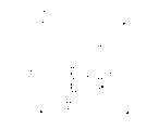
图1示意性地显示可以根据本发明的用作说明的实施例制造的封装微型芯片的局部剖开视图。Figure 1 schematically shows a partial cut-away view of a packaged microchip that may be fabricated according to an illustrative embodiment of the present invention.
图2示意性地显示图1中示出的封装微型芯片沿线2-2截取的的剖面图。FIG. 2 schematically shows a cross-sectional view of the packaged microchip shown in FIG. 1 taken along line 2-2.
图3显示图1和2中所示的封装微型芯片的制造方法。FIG. 3 shows a method of manufacturing the packaged microchip shown in FIGS. 1 and 2 .
具体实施方式Detailed ways
本发明的说明性实施例中,封装微型芯片(例如微型电子机械系统,也被称为“MEMS”)包括将微型芯片固定在封装件内部的绝缘体。选择绝缘体的材料和尺寸,以使由封装件产生的微型芯片应力(例如线性应力和扭曲应力)最小。下面详细描述这个和其它实施例的细节。In an illustrative embodiment of the invention, a packaged microchip (such as a microelectromechanical system, also referred to as "MEMS") includes an insulator that secures the microchip inside the package. The material and dimensions of the insulator are chosen to minimize microchip stresses (eg, linear and torsional stresses) induced by the package. The details of this and other embodiments are described in detail below.
图1示意性地显示用于本发明的不同实施例的封装微型芯片10的部分剖开等距视图。在说明性实施例中,封装微型芯片10是作为陀螺仪的MEMS装置。而且,为了说明的目的,这里公开了作为MEMS陀螺仪的不同的实施例。图1和2表示的MEMS装置确定为陀螺仪10。然而,应该注意到,作为MEMS陀螺仪的不同实施例仅是作为典型例,而不希望限制本发明的所有实施例。因此,一些实施例可以应用到其它类型微型芯片装置,例如集成电路中。另外,本发明的实施例可以应用到其它类型的MEMS装置,例如基于MEMS的光开关装置和基于MEMS的加速计。另外,本发明的实施例可以应用在微型芯片装置中,该微型芯片装置安装在未密封着的封装件内,例如空腔塑料封装件等。Figure 1 schematically shows a partially cut-away isometric view of a packaged
图1所示陀螺仪10包括常规封装件12,气密性地密封封装件12的盖14,和固定在密封着的内部32的常规的陀螺仪电路小片16。陀螺仪电路小片16包括公知的机械结构和测量相对于特定轴的角位置的电子器件(以下相对图2讨论)。从封装件12延伸的若干引脚22与陀螺仪电路小片16电连接,以允许在陀螺仪电子器件和外部装置(例如电脑)之间进行电通信。The
陀螺仪模16不直接连接封装件12的内表面,而是连接绝缘体24,绝缘体自身连接封装件12的内部32。更特别的是,图2示意性地显示图1的封装微型芯片10沿线2-2的剖面图。该图清晰的显示封装件12和它的相应的盖14,电路小片16和绝缘体24。The gyroscope die 16 is not directly attached to the inner surface of the package 12 , but is attached to the
以上提到,电路小片16包括常规的硅MEMS结构18,以机械地感知角旋转,还包括附属电子器件20。该结构18和电子器件20(两者在图2中示意地显示)用作说明地在绝缘硅晶片(silicon-on-insulator)上形成,绝缘硅晶片在一对硅层之间有氧化层。作为一实例,尤其是,MEMS结构18可包括一个或多个通过若干挠曲部分悬置在硅基片26上的振动体(vibrating mass)。该结构18也可以包括梳轮驱动和感知设备,以驱动振动体,并且感知其运动。因此,尤其是,电子器件20可以包括驱动和感知电子器件,它们与梳轮驱动和感知设备结合,和信号传输电路。导线23使附属电子器件20与引脚22电连接。典型的MEMS陀螺仪在待审美国临时专利申请60/364,322和60/354,610中详细描述,两者转让给Analog Devices,Norwood公司,马萨诸塞州。公开的两个提到的临时专利公开内容整体在这里提出作为参考。As mentioned above, die 16 includes conventional
在可选实施例中,MEMS结构18和附属电子器件20在不同的电路小片上。例如,具有MEMS结构的电路小片16可以通过第一绝缘体24安装在封装件12上,同时具有附属电子器件20的电路小片16可以通过第二绝缘体24安装在封装件12上。可选择的,两个电路小片可以安装到相同的绝缘体24上。在某些情况下,其中的一个电路小片(例如应力敏感电路小片16)可以安装在绝缘体24上,同时,另一个电路小片16(例如非应力敏感电路小片16)可以直接安装在封装件12上。然而,应该注意到用作说明的实施例的原理可应用到这样的实施例。In an alternative embodiment, the
作为微型芯片和/或集成电路的电路小片16对线性应力和扭曲应力敏感。在上下文中,术语“敏感的”通常意指当承受应力时,在电路小片16上结构18和/或电子器件20的操作能被妥协。例如以上提出的,施加到电路小片16上的应力可以导致悬置振动体的挠曲部分弯曲或压缩。结果,该振动体可能不按指定的比率和角度振动,这样带来转象差问题。作为进一步的实例,梳轮驱动可能不重合,或电子器件20可以受损,任何这些典型的问题不期望地能破坏通过MEMS电路小片16生成的作为结果的数据。而且,因为这些原因,电路小片16或其它微型芯片可以被称为“应力敏感的”。
为解决与应力有关的问题,绝缘体24由具有一定热膨胀系数的材料形成,该热膨胀系数与封装件12的热膨胀系数相比更接近匹配电路小片16的热膨胀系数。换句话说,绝缘体24的热膨胀系数与封装件12的热膨胀系数相比应该更接近电路小片基片26的热膨胀系数。在用作说明的实施例中,封装件12由陶瓷材料形成,例如氧化铝(AL2O3),其通常具有每摄氏度约7ppm的热膨胀系数。而且,在作为说明的实施例中,基片26是硅,其通常具有每摄氏度约4ppm的热膨胀系数。而且,在作为说明的实施例中,绝缘体24的热膨胀系数接近4而不是7。为此,绝缘体24说明性的由硅形成,它精确的与基片26的材料匹配。这样,绝缘体24具有约4的热膨胀系数。而且,绝缘体24和基片26应该基本上以相同的速率响应温度的变化而膨胀和收缩。在可选择的实施例中,绝缘体24由不同于硅的材料形成。然而,说明性的,该材料具有的热膨胀系数相比封装件12的热膨胀系数更接近基片26的热膨胀系数。To address stress-related issues,
尽管这带来有利的结果,然而,绝缘体24仍接触氧化铝封装件12,这样,遭受以上提到的线性应力。然而,绝缘体24减弱了这种应力,减弱程度应该对电路小片性能的影响最小。Although this brings favorable results, the
在用做说明的实施例中,除了匹配模16和绝缘体的24的材料,还要确定绝缘体的尺寸,以便将扭曲应力的影响减到最小。为此,使绝缘体24和电路小片16的结合表面的尺寸具有接触最小。更特别的是,绝缘体24具有顶面28,该顶面28与电路小片16的底面30结合。绝缘体的顶面28具有的表面积小于电路小片16的底面30的表面积,这样,在电路小片底面30和封装件12之间形成空间。因此,电路小片底面30的较大部分不承受由封装件12产生的正扭曲应力。以基于其热膨胀系数匹配材料的方法类似的方式,选择绝缘体24和电路小片16的相对尺寸的该方法在这里称为“匹配”。In the illustrated embodiment, in addition to matching the materials of the
封装模16的不同零部件的典型的尺寸例如下。注意图2,X方向表示长,Y方向表示高(厚度),Z方向(例如,没有显示但垂直于X和Y方向)表示宽。Typical dimensions of the various components of the packaging die 16 are as follows. Note in Figure 2, the X direction represents length, the Y direction represents height (thickness), and the Z direction (eg, not shown but perpendicular to the X and Y directions) represents width.
封装件12:高:0.12英寸Package 12: Height: 0.12 inches
电路小片16:长:0.170英寸;宽:0.140英寸;高:0.027英寸;Chip 16: length: 0.170 inches; width: 0.140 inches; height: 0.027 inches;
绝缘体24:长0.084英寸;宽:0.084英寸;高:0.026英寸Insulator 24: Length 0.084 inches; Width: 0.084 inches; Height: 0.026 inches
具有这些相对尺寸的封装微型芯片应该满意地实现这里描述的目的。当然,这些尺寸只是示例。因此,其它实施例不限于这些特定尺寸。因此,在以上提到的限制内,封装微型芯片10具有不同尺寸的绝缘体24,封装件12和电路小片16,该封装微型芯片10应该提供对应的应力减弱。在一些实施例中,材料是不匹配的,然而相关的绝缘体24/模16的尺寸如上所述匹配。在其它实施例中,材料是匹配的,然而相关的绝缘体24/模16的尺寸如上所述不匹配。A packaged microchip having these relative dimensions should perform satisfactorily for the purposes described herein. Of course, these dimensions are only examples. Accordingly, other embodiments are not limited to these specific dimensions. Therefore, within the constraints mentioned above, a packaged
在作为说明的实施例中,绝缘体24是硅晶片,该硅晶片借助粘合剂34与电路小片底面30和封装件内表面结合。该粘合剂34优选的具有吸收应力性能,这进一步减弱提到的应力。在典型的实施例中,粘合剂34是镀银玻璃粘附材料,例如编号为QMI3555,由加利福尼亚,圣地亚哥的Dexter Electronic Materials分配的Dexter产品,DexterElectronic Materials是德国的Loctite公司的分公司。In the illustrated embodiment,
其它类型的材料可以用来使绝缘体24与Dexter产品16以及封装件12结合。这样的材料包括其它镀银玻璃材料,环氧树脂类,氰酸盐酯,和硅树脂。在不同的实施例中,尽管希望,但没有必要这些粘接剂具有应力吸收性能。另外,其它常规的装置可以用于使绝缘体24与电路小片16和封装件12连接。因此,粘附剂34的讨论是典型的,并且不希望限制本发明的不同实施例的范围。Other types of materials may be used to
在可选实施例中,绝缘体24与电路小片16成整体,因而相同的材料。在其它实施例中,绝缘体24与封装件12成整体(即绝缘体24结合在封装件内)。在这样的实施例中,绝缘体24和封装件12可由具有更接近模16的热膨胀系数的材料制造。例如,封装件12可以由氮化铝(AlN)制造。In an alternative embodiment,
图3显示如图1和2所示的封装微型芯片10的典型封装方法。该方法从步骤300开始,其中粘附剂34使绝缘体24与封装件12的内表面结合。如本领域的普通技术人员所知,内表面通常被称为“电路小片附着垫”。该方法继续到步骤302,其中基片26的底面30与绝缘体24的顶面28结合。接着,电路小片16与封装件12电互连(步骤304)。接着,在步骤306,盖14固定到封装件12的顶部,从而来密封内部32。如果需要,在盖14紧固在封装件12上之前,可以将气体注入封装件内部32内。FIG. 3 shows a typical packaging method for packaging the
在可选择的实施例中,步骤300和302以相反顺序实施。换句话说,在这样的实施例中,绝缘体24首先与基片26结合,接着绝缘体24(具有连接的基片26)与封装件12的内部32结合。In an alternative embodiment, steps 300 and 302 are performed in reverse order. In other words, in such an embodiment,
尽管这里公开了本发明的不同的典型实施例,本领域的普通技术人员显然可知,在不超出本发明的实质范围的前提下,不同的改变和修改同样可以实现本发明的一些优点。Although various exemplary embodiments of this invention have been disclosed herein, it will be apparent to those skilled in the art that various changes and modifications can be made to achieve some of the advantages of this invention without departing from the essential scope of this invention.
Claims (19)
Applications Claiming Priority (2)
| Application Number | Priority Date | Filing Date | Title |
|---|---|---|---|
| US10/234,215US6768196B2 (en) | 2002-09-04 | 2002-09-04 | Packaged microchip with isolation |
| US10/234,215 | 2002-09-04 |
Publications (2)
| Publication Number | Publication Date |
|---|---|
| CN1678513A CN1678513A (en) | 2005-10-05 |
| CN100408470Ctrue CN100408470C (en) | 2008-08-06 |
Family
ID=31977372
Family Applications (1)
| Application Number | Title | Priority Date | Filing Date |
|---|---|---|---|
| CNB038210754AExpired - Fee RelatedCN100408470C (en) | 2002-09-04 | 2003-09-04 | Microchip with thermal stress relief |
Country Status (6)
| Country | Link |
|---|---|
| US (1) | US6768196B2 (en) |
| EP (1) | EP1534624A1 (en) |
| JP (1) | JP2005538551A (en) |
| CN (1) | CN100408470C (en) |
| AU (1) | AU2003270331A1 (en) |
| WO (1) | WO2004022477A1 (en) |
Families Citing this family (52)
| Publication number | Priority date | Publication date | Assignee | Title |
|---|---|---|---|---|
| TW588532B (en)* | 2002-03-29 | 2004-05-21 | Realtek Semiconductor Corp | Management device and method of NAT/NAPT session |
| US20040041254A1 (en)* | 2002-09-04 | 2004-03-04 | Lewis Long | Packaged microchip |
| US7166911B2 (en) | 2002-09-04 | 2007-01-23 | Analog Devices, Inc. | Packaged microchip with premolded-type package |
| US6946742B2 (en)* | 2002-12-19 | 2005-09-20 | Analog Devices, Inc. | Packaged microchip with isolator having selected modulus of elasticity |
| US20050056870A1 (en)* | 2002-12-19 | 2005-03-17 | Karpman Maurice S. | Stress sensitive microchip with premolded-type package |
| KR100622372B1 (en) | 2004-06-01 | 2006-09-19 | 삼성전자주식회사 | Gyro sensor comprising a plurality of configuration units and a manufacturing method thereof |
| CN100406373C (en)* | 2004-07-07 | 2008-07-30 | 日月光半导体制造股份有限公司 | Micro-mirror element packaging structure |
| US7262493B2 (en)* | 2005-01-06 | 2007-08-28 | Avago Technologies General Ip (Singapore) Pte. Ltd. | System and method for mounting electrical devices |
| JP4740678B2 (en)* | 2005-07-27 | 2011-08-03 | Okiセミコンダクタ株式会社 | Semiconductor device |
| US20090095076A1 (en)* | 2005-08-18 | 2009-04-16 | Yasuhiro Tamura | Acceleration Sensor Device and Sensor Apparatus |
| US8129801B2 (en)* | 2006-01-06 | 2012-03-06 | Honeywell International Inc. | Discrete stress isolator attachment structures for MEMS sensor packages |
| JP2008008634A (en) | 2006-06-27 | 2008-01-17 | Fujitsu Media Device Kk | Angular velocity sensor |
| WO2008003051A2 (en)* | 2006-06-29 | 2008-01-03 | Analog Devices, Inc. | Stress mitigation in packaged microchips |
| US8159059B2 (en)* | 2006-08-25 | 2012-04-17 | Kyocera Corporation | Microelectromechanical device and method for manufacturing the same |
| US20080222884A1 (en)* | 2007-03-14 | 2008-09-18 | Honeywell International Inc. | Packaging for chip-on-board pressure sensor |
| US7694610B2 (en)* | 2007-06-27 | 2010-04-13 | Siemens Medical Solutions Usa, Inc. | Photo-multiplier tube removal tool |
| US7798010B2 (en)* | 2007-10-11 | 2010-09-21 | Honeywell International Inc. | Sensor geometry for improved package stress isolation |
| US7830003B2 (en)* | 2007-12-27 | 2010-11-09 | Honeywell International, Inc. | Mechanical isolation for MEMS devices |
| US8257119B2 (en)* | 2008-12-19 | 2012-09-04 | Honeywell International | Systems and methods for affixing a silicon device to a support structure |
| US8614491B2 (en)* | 2009-04-07 | 2013-12-24 | Honeywell International Inc. | Package interface plate for package isolation structures |
| US20110042137A1 (en)* | 2009-08-18 | 2011-02-24 | Honeywell International Inc. | Suspended lead frame electronic package |
| US9215519B2 (en) | 2010-07-30 | 2015-12-15 | Invensense, Inc. | Reduced footprint microphone system with spacer member having through-hole |
| US8803262B2 (en) | 2012-01-17 | 2014-08-12 | Rosemount Aerospace Inc. | Die attach stress isolation |
| US8866274B2 (en) | 2012-03-27 | 2014-10-21 | Infineon Technologies Ag | Semiconductor packages and methods of formation thereof |
| US9212908B2 (en) | 2012-04-26 | 2015-12-15 | Analog Devices, Inc. | MEMS gyroscopes with reduced errors |
| US9686864B2 (en) | 2012-07-31 | 2017-06-20 | Hewlett-Packard Development Company, L.P. | Device including interposer between semiconductor and substrate |
| US8841738B2 (en) | 2012-10-01 | 2014-09-23 | Invensense, Inc. | MEMS microphone system for harsh environments |
| US9676614B2 (en) | 2013-02-01 | 2017-06-13 | Analog Devices, Inc. | MEMS device with stress relief structures |
| DE102013101732A1 (en)* | 2013-02-21 | 2014-08-21 | Epcos Ag | sensor system |
| DE102013101731A1 (en) | 2013-02-21 | 2014-09-04 | Epcos Ag | Pressure Sensor System |
| JP2015002314A (en)* | 2013-06-18 | 2015-01-05 | セイコーエプソン株式会社 | Electronic device, electronic apparatus, and mobile |
| EP2947692B1 (en) | 2013-12-20 | 2020-09-23 | Analog Devices, Inc. | Integrated device die and package with stress reduction features |
| US9731959B2 (en)* | 2014-09-25 | 2017-08-15 | Analog Devices, Inc. | Integrated device packages having a MEMS die sealed in a cavity by a processor die and method of manufacturing the same |
| US10167189B2 (en) | 2014-09-30 | 2019-01-01 | Analog Devices, Inc. | Stress isolation platform for MEMS devices |
| CN105712283B (en)* | 2014-12-02 | 2018-07-31 | 北京自动化控制设备研究所 | A stress relief structure for LCC packaging |
| DE102014119396A1 (en)* | 2014-12-22 | 2016-06-23 | Endress + Hauser Gmbh + Co. Kg | Pressure measuring device |
| US10287161B2 (en) | 2015-07-23 | 2019-05-14 | Analog Devices, Inc. | Stress isolation features for stacked dies |
| US10131538B2 (en) | 2015-09-14 | 2018-11-20 | Analog Devices, Inc. | Mechanically isolated MEMS device |
| ITUB20154017A1 (en)* | 2015-09-30 | 2017-03-30 | St Microelectronics Srl | ENCAPSULATED DEVICE OF SEMICONDUCTOR MATERIAL WITH REDUCED SENSITIVITY TOWARDS THERMO-MECHANICAL STRESS |
| DE102015117736A1 (en)* | 2015-10-19 | 2017-04-20 | Endress+Hauser Gmbh+Co. Kg | Pressure measuring device |
| US10278281B1 (en)* | 2015-10-30 | 2019-04-30 | Garmin International, Inc. | MEMS stress isolation and stabilization system |
| JP2017125753A (en) | 2016-01-13 | 2017-07-20 | セイコーエプソン株式会社 | Electronic device, electronic apparatus, and moving body |
| CN105668507A (en)* | 2016-01-22 | 2016-06-15 | 中国科学院地质与地球物理研究所 | Encapsulation structure and encapsulation method of MEMS (Micro-Electro-Mechanical System) chip |
| US11127716B2 (en) | 2018-04-12 | 2021-09-21 | Analog Devices International Unlimited Company | Mounting structures for integrated device packages |
| CN108622847A (en)* | 2018-05-03 | 2018-10-09 | 河北美泰电子科技有限公司 | The encapsulating method and structure of MEMS sensor |
| US11417611B2 (en) | 2020-02-25 | 2022-08-16 | Analog Devices International Unlimited Company | Devices and methods for reducing stress on circuit components |
| US11981560B2 (en) | 2020-06-09 | 2024-05-14 | Analog Devices, Inc. | Stress-isolated MEMS device comprising substrate having cavity and method of manufacture |
| US11664340B2 (en) | 2020-07-13 | 2023-05-30 | Analog Devices, Inc. | Negative fillet for mounting an integrated device die to a carrier |
| RU2748290C1 (en)* | 2020-09-15 | 2021-05-21 | Акционерное общество "Инерциальные технологии "Технокомплекса" (АО "ИТТ") | Micromechanical accelerometer sensor element |
| CN114804006A (en)* | 2021-01-29 | 2022-07-29 | 华为技术有限公司 | Packaging structure, substrate and packaging method |
| CN114112120A (en)* | 2021-11-12 | 2022-03-01 | 南京英锐创电子科技有限公司 | Sensor package structure and method |
| CN115285934B (en)* | 2022-08-10 | 2024-11-15 | 河北美泰电子科技有限公司 | An assembly method and assembly housing for solving welding stress of MEMS inertial chip |
Citations (5)
| Publication number | Priority date | Publication date | Assignee | Title |
|---|---|---|---|---|
| US4872047A (en)* | 1986-11-07 | 1989-10-03 | Olin Corporation | Semiconductor die attach system |
| US5241133A (en)* | 1990-12-21 | 1993-08-31 | Motorola, Inc. | Leadless pad array chip carrier |
| US5273939A (en)* | 1991-03-09 | 1993-12-28 | Robert Bosch Gmbh | Method of assembling micromechanical sensors |
| US5994161A (en)* | 1997-09-03 | 1999-11-30 | Motorola, Inc. | Temperature coefficient of offset adjusted semiconductor device and method thereof |
| US20010055836A1 (en)* | 2000-06-26 | 2001-12-27 | Tomohito Kunda | Semiconductor dynamic sensor and method of manufacturing the same |
Family Cites Families (12)
| Publication number | Priority date | Publication date | Assignee | Title |
|---|---|---|---|---|
| US4710744A (en)* | 1985-04-08 | 1987-12-01 | Honeywell Inc. | Pressure transducer package |
| US4800758A (en)* | 1986-06-23 | 1989-01-31 | Rosemount Inc. | Pressure transducer with stress isolation for hard mounting |
| US4948757A (en)* | 1987-04-13 | 1990-08-14 | General Motors Corporation | Method for fabricating three-dimensional microstructures and a high-sensitivity integrated vibration sensor using such microstructures |
| US4740410A (en)* | 1987-05-28 | 1988-04-26 | The Regents Of The University Of California | Micromechanical elements and methods for their fabrication |
| US4918032A (en)* | 1988-04-13 | 1990-04-17 | General Motors Corporation | Method for fabricating three-dimensional microstructures and a high-sensitivity integrated vibration sensor using such microstructures |
| US5105258A (en)* | 1990-11-21 | 1992-04-14 | Motorola, Inc. | Metal system for semiconductor die attach |
| JPH04258176A (en)* | 1991-02-12 | 1992-09-14 | Mitsubishi Electric Corp | semiconductor pressure sensor |
| US5315155A (en) | 1992-07-13 | 1994-05-24 | Olin Corporation | Electronic package with stress relief channel |
| IL106790A (en)* | 1992-09-01 | 1996-08-04 | Rosemount Inc | Pedestal mount capacitive pressure sensor and a process of manufacturing same |
| US5336928A (en)* | 1992-09-18 | 1994-08-09 | General Electric Company | Hermetically sealed packaged electronic system |
| US5468999A (en)* | 1994-05-26 | 1995-11-21 | Motorola, Inc. | Liquid encapsulated ball grid array semiconductor device with fine pitch wire bonding |
| US5945605A (en)* | 1997-11-19 | 1999-08-31 | Sensym, Inc. | Sensor assembly with sensor boss mounted on substrate |
- 2002
- 2002-09-04USUS10/234,215patent/US6768196B2/ennot_activeExpired - Lifetime
- 2003
- 2003-09-04JPJP2004534620Apatent/JP2005538551A/enactivePending
- 2003-09-04EPEP03752017Apatent/EP1534624A1/ennot_activeWithdrawn
- 2003-09-04AUAU2003270331Apatent/AU2003270331A1/ennot_activeAbandoned
- 2003-09-04WOPCT/US2003/027815patent/WO2004022477A1/enactiveApplication Filing
- 2003-09-04CNCNB038210754Apatent/CN100408470C/ennot_activeExpired - Fee Related
Patent Citations (5)
| Publication number | Priority date | Publication date | Assignee | Title |
|---|---|---|---|---|
| US4872047A (en)* | 1986-11-07 | 1989-10-03 | Olin Corporation | Semiconductor die attach system |
| US5241133A (en)* | 1990-12-21 | 1993-08-31 | Motorola, Inc. | Leadless pad array chip carrier |
| US5273939A (en)* | 1991-03-09 | 1993-12-28 | Robert Bosch Gmbh | Method of assembling micromechanical sensors |
| US5994161A (en)* | 1997-09-03 | 1999-11-30 | Motorola, Inc. | Temperature coefficient of offset adjusted semiconductor device and method thereof |
| US20010055836A1 (en)* | 2000-06-26 | 2001-12-27 | Tomohito Kunda | Semiconductor dynamic sensor and method of manufacturing the same |
Also Published As
| Publication number | Publication date |
|---|---|
| US20040041248A1 (en) | 2004-03-04 |
| US6768196B2 (en) | 2004-07-27 |
| AU2003270331A1 (en) | 2004-03-29 |
| WO2004022477A1 (en) | 2004-03-18 |
| CN1678513A (en) | 2005-10-05 |
| JP2005538551A (en) | 2005-12-15 |
| EP1534624A1 (en) | 2005-06-01 |
Similar Documents
| Publication | Publication Date | Title |
|---|---|---|
| CN100408470C (en) | Microchip with thermal stress relief | |
| US20040041254A1 (en) | Packaged microchip | |
| US6946742B2 (en) | Packaged microchip with isolator having selected modulus of elasticity | |
| US7166911B2 (en) | Packaged microchip with premolded-type package | |
| US7370530B2 (en) | Package for MEMS devices | |
| US7563632B2 (en) | Methods for packaging and sealing an integrated circuit die | |
| US6621158B2 (en) | Package for sealing an integrated circuit die | |
| CN103221332B (en) | Reduce the encapsulation of the stress on MEMS | |
| US20170073218A1 (en) | Mechanically Isolated MEMS Device | |
| CN112225168B (en) | A stress isolation packaging structure for MEMS devices | |
| JP2005528995A (en) | Micromachining type component and corresponding manufacturing method | |
| EP3597590B1 (en) | Sensor packages | |
| EP2004543A2 (en) | Mems device package with thermally compliant insert | |
| US20050056870A1 (en) | Stress sensitive microchip with premolded-type package | |
| EP3614103B1 (en) | Sensor packages | |
| Wang | Considerations for mems packaging | |
| JP6462128B2 (en) | Semiconductor device | |
| Wilde | 30 Years of Sensors' Assembly and Packaging 1988 to 2018. | |
| CN101258408A (en) | Acceleration sensor device |
Legal Events
| Date | Code | Title | Description |
|---|---|---|---|
| C06 | Publication | ||
| PB01 | Publication | ||
| C10 | Entry into substantive examination | ||
| SE01 | Entry into force of request for substantive examination | ||
| C14 | Grant of patent or utility model | ||
| GR01 | Patent grant | ||
| C56 | Change in the name or address of the patentee | Owner name:AMERICA ANALOG DEVICE INC. Free format text:FORMER NAME: ANALOG DEVICES INC. | |
| CP01 | Change in the name or title of a patent holder | Address after:Massachusetts, USA Patentee after:ANALOG DEVICES, Inc. Address before:Massachusetts, USA Patentee before:ANALOG DEVICES, Inc. | |
| CF01 | Termination of patent right due to non-payment of annual fee | ||
| CF01 | Termination of patent right due to non-payment of annual fee | Granted publication date:20080806 |