CN100407427C - NROM memory element, memory array, related apparatus and method - Google Patents
NROM memory element, memory array, related apparatus and methodDownload PDFInfo
- Publication number
- CN100407427C CN100407427CCN038196913ACN03819691ACN100407427CCN 100407427 CCN100407427 CCN 100407427CCN 038196913 ACN038196913 ACN 038196913ACN 03819691 ACN03819691 ACN 03819691ACN 100407427 CCN100407427 CCN 100407427C
- Authority
- CN
- China
- Prior art keywords
- source
- gate
- region
- vertical
- array
- Prior art date
- Legal status (The legal status is an assumption and is not a legal conclusion. Google has not performed a legal analysis and makes no representation as to the accuracy of the status listed.)
- Expired - Lifetime
Links
Images


Classifications
- H—ELECTRICITY
- H10—SEMICONDUCTOR DEVICES; ELECTRIC SOLID-STATE DEVICES NOT OTHERWISE PROVIDED FOR
- H10D—INORGANIC ELECTRIC SEMICONDUCTOR DEVICES
- H10D84/00—Integrated devices formed in or on semiconductor substrates that comprise only semiconducting layers, e.g. on Si wafers or on GaAs-on-Si wafers
- H—ELECTRICITY
- H10—SEMICONDUCTOR DEVICES; ELECTRIC SOLID-STATE DEVICES NOT OTHERWISE PROVIDED FOR
- H10D—INORGANIC ELECTRIC SEMICONDUCTOR DEVICES
- H10D30/00—Field-effect transistors [FET]
- H10D30/60—Insulated-gate field-effect transistors [IGFET]
- H10D30/69—IGFETs having charge trapping gate insulators, e.g. MNOS transistors
- H10D30/693—Vertical IGFETs having charge trapping gate insulators
- G—PHYSICS
- G11—INFORMATION STORAGE
- G11C—STATIC STORES
- G11C11/00—Digital stores characterised by the use of particular electric or magnetic storage elements; Storage elements therefor
- G11C11/56—Digital stores characterised by the use of particular electric or magnetic storage elements; Storage elements therefor using storage elements with more than two stable states represented by steps, e.g. of voltage, current, phase, frequency
- G11C11/5692—Digital stores characterised by the use of particular electric or magnetic storage elements; Storage elements therefor using storage elements with more than two stable states represented by steps, e.g. of voltage, current, phase, frequency read-only digital stores using storage elements with more than two stable states
- G—PHYSICS
- G11—INFORMATION STORAGE
- G11C—STATIC STORES
- G11C16/00—Erasable programmable read-only memories
- G11C16/02—Erasable programmable read-only memories electrically programmable
- G11C16/04—Erasable programmable read-only memories electrically programmable using variable threshold transistors, e.g. FAMOS
- G11C16/0466—Erasable programmable read-only memories electrically programmable using variable threshold transistors, e.g. FAMOS comprising cells with charge storage in an insulating layer, e.g. metal-nitride-oxide-silicon [MNOS], silicon-oxide-nitride-oxide-silicon [SONOS]
- G11C16/0475—Erasable programmable read-only memories electrically programmable using variable threshold transistors, e.g. FAMOS comprising cells with charge storage in an insulating layer, e.g. metal-nitride-oxide-silicon [MNOS], silicon-oxide-nitride-oxide-silicon [SONOS] comprising two or more independent storage sites which store independent data
- H—ELECTRICITY
- H10—SEMICONDUCTOR DEVICES; ELECTRIC SOLID-STATE DEVICES NOT OTHERWISE PROVIDED FOR
- H10B—ELECTRONIC MEMORY DEVICES
- H10B20/00—Read-only memory [ROM] devices
- H—ELECTRICITY
- H10—SEMICONDUCTOR DEVICES; ELECTRIC SOLID-STATE DEVICES NOT OTHERWISE PROVIDED FOR
- H10B—ELECTRONIC MEMORY DEVICES
- H10B41/00—Electrically erasable-and-programmable ROM [EEPROM] devices comprising floating gates
- H10B41/20—Electrically erasable-and-programmable ROM [EEPROM] devices comprising floating gates characterised by three-dimensional arrangements, e.g. with cells on different height levels
- H10B41/23—Electrically erasable-and-programmable ROM [EEPROM] devices comprising floating gates characterised by three-dimensional arrangements, e.g. with cells on different height levels with source and drain on different levels, e.g. with sloping channels
- H10B41/27—Electrically erasable-and-programmable ROM [EEPROM] devices comprising floating gates characterised by three-dimensional arrangements, e.g. with cells on different height levels with source and drain on different levels, e.g. with sloping channels the channels comprising vertical portions, e.g. U-shaped channels
- H—ELECTRICITY
- H10—SEMICONDUCTOR DEVICES; ELECTRIC SOLID-STATE DEVICES NOT OTHERWISE PROVIDED FOR
- H10B—ELECTRONIC MEMORY DEVICES
- H10B43/00—EEPROM devices comprising charge-trapping gate insulators
- H10B43/20—EEPROM devices comprising charge-trapping gate insulators characterised by three-dimensional arrangements, e.g. with cells on different height levels
- H10B43/23—EEPROM devices comprising charge-trapping gate insulators characterised by three-dimensional arrangements, e.g. with cells on different height levels with source and drain on different levels, e.g. with sloping channels
- H10B43/27—EEPROM devices comprising charge-trapping gate insulators characterised by three-dimensional arrangements, e.g. with cells on different height levels with source and drain on different levels, e.g. with sloping channels the channels comprising vertical portions, e.g. U-shaped channels
- H—ELECTRICITY
- H10—SEMICONDUCTOR DEVICES; ELECTRIC SOLID-STATE DEVICES NOT OTHERWISE PROVIDED FOR
- H10D—INORGANIC ELECTRIC SEMICONDUCTOR DEVICES
- H10D30/00—Field-effect transistors [FET]
- H10D30/60—Insulated-gate field-effect transistors [IGFET]
- H10D30/68—Floating-gate IGFETs
- H10D30/689—Vertical floating-gate IGFETs
- H—ELECTRICITY
- H10—SEMICONDUCTOR DEVICES; ELECTRIC SOLID-STATE DEVICES NOT OTHERWISE PROVIDED FOR
- H10D—INORGANIC ELECTRIC SEMICONDUCTOR DEVICES
- H10D30/00—Field-effect transistors [FET]
- H10D30/60—Insulated-gate field-effect transistors [IGFET]
- H10D30/69—IGFETs having charge trapping gate insulators, e.g. MNOS transistors
- H10D30/691—IGFETs having charge trapping gate insulators, e.g. MNOS transistors having more than two programming levels
- B—PERFORMING OPERATIONS; TRANSPORTING
- B82—NANOTECHNOLOGY
- B82Y—SPECIFIC USES OR APPLICATIONS OF NANOSTRUCTURES; MEASUREMENT OR ANALYSIS OF NANOSTRUCTURES; MANUFACTURE OR TREATMENT OF NANOSTRUCTURES
- B82Y10/00—Nanotechnology for information processing, storage or transmission, e.g. quantum computing or single electron logic
Landscapes
- Engineering & Computer Science (AREA)
- Microelectronics & Electronic Packaging (AREA)
- Computer Hardware Design (AREA)
- Semiconductor Memories (AREA)
- Non-Volatile Memory (AREA)
Abstract
Description
Translated fromChinese技术领域technical field
本发明涉及NROM存储器元件,这样的存储器元件的阵列,应用这样的存储器元件和阵列的电子装置以及和这样的存储器元件相关的方法。The present invention relates to NROM memory elements, arrays of such memory elements, electronic devices employing such memory elements and arrays, and methods related to such memory elements.
背景技术Background technique
电子系统应用了各种类型的存储器器件。诸如DRAM(动态随机存取存储器)的某些类型的存储器器件提供了许多低功耗小尺寸的可读可写的数据存储器件,但是这些类型的存储器件没有其他类型那样快的存取速度及仅提供易失的数据存储能力。易失的数据存储意味着为了保持数据存储器必须被连续供电,当电源中断,存储的数据就丢失。非易失存储器能不需要电源保持数据。Electronic systems employ various types of memory devices. Certain types of memory devices such as DRAM (Dynamic Random Access Memory) provide many readable and writable data storage devices with low power consumption and small size, but these types of memory devices do not have as fast access speed and Provides only volatile data storage capacity. Volatile data storage means that the memory must be continuously powered in order to maintain the data, and when the power is interrupted, the stored data is lost. Nonvolatile memory can retain data without requiring power.
其他类型的存储器能提供只读或读写能力以及非易失数据存储装置,但运行慢得多。这些类型包括CD-ROM器件,CD-WROM器件,磁数据存储装置(硬盘,软盘,磁带等),磁光装置等。Other types of memory provide read-only or read-write capabilities and nonvolatile data storage, but operate much slower. These types include CD-ROM devices, CD-WROM devices, magnetic data storage devices (hard disks, floppy disks, magnetic tape, etc.), magneto-optical devices, and the like.
还有其他类型的存储器提供非常快的运行速度,但也要求高的能耗。静态RAM或SRAM是这样的存储器器件的一个实例。There are other types of memory that provide very fast operating speeds, but also require high power consumption. Static RAM or SRAM is one example of such a memory device.
在大多数计算机中混用了不同类型的存储器以选择性地获得每种技术能提供的优点。例如,只读存储器或ROM,EEPROM等被典型地用于存储有限数量的相对非频繁存取的诸如基础输入-输出系统的数据。这些存储器被用于响应电源的接通状态存储数据,使处理器被配置成能从诸如硬盘的高容量非易失存储装置装载许多诸如操作系统的软件。操作系统和应用软件通常从高容量存储装置读出,相应的图象则存储在DRAM中。In most computers different types of memory are mixed to selectively take advantage of what each technology can offer. For example, read-only memory or ROM, EEPROM, etc. are typically used to store limited amounts of data that are accessed relatively infrequently, such as underlying input-output systems. These memories are used to store data in response to an on state of power, enabling the processor to be configured to load a large amount of software, such as an operating system, from a high capacity non-volatile storage device such as a hard disk. The operating system and application software are usually read from a high-capacity storage device, and the corresponding images are stored in DRAM.
当处理器执行指令时,某些类型的数据可从存储器反复读出。结果,某些SRAM或其他高速存储器通常被提供作为和处理器相结合的“高速缓冲存储器”,并可被包括在处理器集成电路或芯片中或非常靠近该集成电路或芯片。Certain types of data are repeatedly read from memory as the processor executes instructions. As a result, some SRAM or other high speed memory is often provided as "cache memory" in conjunction with the processor and may be included on or in close proximity to the processor integrated circuit or chip.
在大多数现代计算装置以及包括自动的和/或可编程的装置(家庭娱乐装置,电信装置,自动控制系统等)的很多类型应用中都包含几种不同类型的存储器。当系统和软件复杂程度增加时,对附加的存储器的需求也增加。对可携带性,计算能力和/或实用性的要求导致在减少功耗和每比特电路面积方面不断增加的压力。Several different types of memory are included in most modern computing devices and in many types of applications including automotive and/or programmable devices (home entertainment devices, telecommunications devices, automatic control systems, etc.). As system and software complexity increases, so does the need for additional memory. Requirements for portability, computing power, and/or practicality lead to ever-increasing pressure to reduce power consumption and circuit area per bit.
部分地由于存储器元件能被制造成具有非常小的面积,并且使每元件所需的功率相当小,DRAM已经被开发成具有非常高的容量。因此,这使存储器集成电路被制成在每个芯片中能集成数百万个存储器元件。典型的单晶体管单电容器DRAM存储器元件可以被做得只有极端小的面积要求。DRAMs have been developed to have very high capacities, in part because memory elements can be fabricated with very small areas and require relatively little power per element. Thus, this enables memory integrated circuits to be fabricated integrating millions of memory elements per chip. Typical single-transistor single-capacitor DRAM memory elements can be made with extremely small area requirements.
这样的面积通常等于约3F×2F或更小,这里“F”被定义为等于最小节距的一半(见下文的图4)。最小节距(即“P”)被定义为等于最小线宽(即“W”)加上阵列的重复图形中一个线条和靠近的相邻线条之间在该线条一侧直接相邻于该线条的间隔的宽度(即“S”)。这样,在很多实施中,所给出的DRAM元件消耗的面积不大于约8F2。Such an area is typically equal to about 3F x 2F or less, where "F" is defined as equal to half the minimum pitch (see Figure 4 below). The minimum pitch (i.e. "P") is defined as equal to the minimum line width (i.e. "W") plus the repeating pattern of the array between a line and the next adjacent line immediately adjacent to the line on one side of the line The width of the interval (ie "S"). Thus, in many implementations, a given DRAM element consumes no more than about8F2 of area.
但是,因为DRAM是易失存储器器件,要求“刷新”操作。在刷新操作中,数据从每个存储器元件中读出,放大并写回DRAM。作为第一个结果,在刷新操作期间DRAM电路通常不可进行其他类型的存储器操作。另外,刷新操作周期性地进行导致存在这样的时间,在该时间内数据不能方便地从DRAM读取或写入DRAM。作为第二个结果,在DRAM中存储数据总是需要一定数量的电能。However, because DRAM is a volatile memory device, a "refresh" operation is required. In a refresh operation, data is read from each memory element, amplified and written back to the DRAM. As a first result, other types of memory operations are generally not available to DRAM circuits during refresh operations. In addition, refresh operations are performed periodically resulting in times during which data cannot be conveniently read from or written to the DRAM. As a second consequence, storing data in DRAM always requires a certain amount of electrical energy.
作为第三个结果,诸如各种个人计算机的计算机的引导程序的操作包括一个电源接通以后计算机并不能使用的时间周期。在该周期中,操作系统指令和相关数据以及应用指令和相关数据从诸如常规的磁盘驱动器的相对慢的非易失存储器读出,由处理单元解码,结果的指令和相关数据被装载入结合诸如DRAM的可相对迅速存取但易失的存储器的模块中。其他的结果从包括在各种电子装置中的存储器系统的各种性能中产生,为这些结果还需应用更加复杂的软件,但这些实例仅用作说明运行中的各种需要。As a third result, the operation of the boot program of computers such as various personal computers includes a period of time after the power is turned on and the computer cannot be used. During this cycle, operating system instructions and associated data, as well as application instructions and associated data, are read from relatively slow non-volatile memory such as a conventional disk drive, decoded by the processing unit, and the resulting instructions and associated data loaded into the combined In modules of relatively quickly accessible but volatile memory such as DRAM. Other results arise from the various properties of the memory systems included in the various electronic devices, for which more complex software has to be applied, but these examples serve only to illustrate the various needs in operation.
这样就需要和提供高单位面积数据存储容量,重新编程能力,低功耗和相对高数据存取速度的非易失存储器相关的装置和方法。There is thus a need for apparatus and methods associated with non-volatile memories that provide high data storage capacity per unit area, reprogrammability, low power consumption, and relatively high data access speeds.
发明内容Contents of the invention
本发明在第一方面包括一种制造设计成每一个F2存储至少一比特的存储器元件阵列的方法。该方法包括在半导体衬底的第一区域进行掺杂并切割衬底以提供基本垂直的边缘表面阵列。多对边缘表面互相面对并相隔和边缘阵列的节距的一半相等的距离。该方法还包括掺杂多对边缘表面之间的第二区域并在至少一部分各个边缘表面上设置各个结构,其中,所述结构包括被设计成每栅储存多于一比特的栅,每一个结构都提供电子存储器的功能。该方法还包括向第一和第二区域建立电接触。The invention comprises in a first aspect a method of fabricating an array of memory elements designed to store at least one bit eachF2 . The method includes doping a first region of a semiconductor substrate and cutting the substrate to provide an array of substantially vertical edge surfaces. Pairs of edge surfaces face each other and are separated by a distance equal to half the pitch of the edge array. The method also includes doping a second region between pairs of edge surfaces and disposing respective structures on at least a portion of each edge surface, wherein the structures include gates designed to store more than one bit per gate, each structure Both provide the function of electronic memory. The method also includes establishing electrical contact to the first and second regions.
本发明在另一方面包括一种制造设计成每一个F2存储至少一比特的存储器元件阵列的方法。该方法包括设置提供电子存储器功能,相隔和阵列的最小节距的一半相等的距离的基本垂直的结构,其中,所述结构包括被设计成每栅储存多于一比特的栅,并向包括垂直结构的存储器元件建立电接触。Another aspect of the invention includes a method of fabricating an array of memory elements designed to store at least one bit perF2 . The method includes arranging substantially vertical structures providing electronic memory functionality spaced apart at a distance equal to half the minimum pitch of the array, wherein the structures include gates designed to store more than one bit per gate, and towards the vertical The memory elements of the structure establish electrical contact.
本发明在还有一个方面包括一种设计成每一个F2存储至少一比特的存储器元件阵列,该阵列用提供电子存储器功能,相隔和阵列的最小节距的一半相等的距离的垂直结构形成。提供电子存储器功能的结构设计成每一门存储量多于一比特。该阵列也包括向包括垂直结构的存储器元件建立的电接触。The invention comprises, in yet another aspect, an array of memory elements designed to store at least one bit eachF2 , the array being formed with vertical structures providing electronic memory functionality spaced a distance equal to half the minimum pitch of the array. Architectures providing electronic memory functions are designed to store more than one bit per gate. The array also includes electrical contacts established to memory elements including vertical structures.
本发明在还有一个方面包括一种从衬底向外延伸的金属氧化物半导体场效应晶体管(MOSFET),该MOSFET具有第一源/漏区域,第二源/漏区域,第一和第二源/漏区域之间的沟道区域,和由栅绝缘体与沟道区域分离的栅。源线形成在和垂直MOSFET毗邻的沟槽中,其中第一源/漏区域被连接到该源线。传输线被连接到第二源/漏区域。这能使可编程MOSFET具有陷于和第一源/漏区域毗邻的栅绝缘体中的众多电荷水平中的一个水平,使沟道区域具有第一电压阈值区域(Vt1)和第二电压阈值区域(Vt2),使可编程MOSFET运行时的源漏电流降低。In yet another aspect, the invention includes a metal oxide semiconductor field effect transistor (MOSFET) extending outwardly from a substrate, the MOSFET having a first source/drain region, a second source/drain region, first and second A channel region between the source/drain regions, and a gate separated from the channel region by a gate insulator. A source line is formed in the trench adjacent to the vertical MOSFET, wherein the first source/drain region is connected to the source line. The transmission line is connected to the second source/drain region. This enables a programmable MOSFET with one of many levels of charge trapped in the gate insulator adjacent to the first source/drain region, enabling the channel region to have a first voltage threshold region (Vt1) and a second voltage threshold region (Vt2 ), allowing the programmable MOSFET to operate with reduced source-drain current.
本发明的这些以及其他实施例,方面,优点和特征部分将在下文的叙述中阐明,部分通过参考对本发明的下文的叙述和被参考的附图或通过本发明的实践对于业内的熟练人士而言是显而易见的。本发明的这些方面,优点和特征通过在附后的权利要求中指出的手段,程序及其具体组合实现和获得。These and other embodiments, aspects, advantages and features of the invention will be set forth in part in the following description, and in part will be apparent to those skilled in the art by reference to the following description of the invention and the referenced drawings or by practice of the invention. Words are obvious. The aspects, advantages and features of the invention are realized and obtained by means of the instrumentalities, procedures and specific combinations thereof pointed out in the appended claims.
附图说明Description of drawings
下文将参考下列附图叙述本发明的各个实施例。Various embodiments of the present invention will be described below with reference to the following drawings.
图1是在根据本发明的一个实施例的工艺的一个阶段中半导体衬底部分简化截面侧视图。1 is a simplified cross-sectional side view of a portion of a semiconductor substrate at one stage of a process according to one embodiment of the present invention.
图2是在根据本发明的一个实施例的工艺的一个后继阶段中图1的衬底部分的简化截面侧视图。Figure 2 is a simplified cross-sectional side view of the substrate portion of Figure 1 at a subsequent stage of the process according to one embodiment of the present invention.
图3是在根据本发明的一个实施例的工艺的一个后继阶段中图2的衬底部分简化截面侧视图。Figure 3 is a simplified cross-sectional side view of the substrate portion of Figure 2 at a subsequent stage of the process according to one embodiment of the present invention.
图4是显示根据本发明的一个实施例的存储器元件阵列的一部分的衬底部分的简化平面图。Figure 4 is a simplified plan view of a substrate portion showing a portion of an array of memory elements according to one embodiment of the present invention.
图5是说明根据本发明的一个实施例的图1-3的结构和图4的平面图之间的关系的简化截面侧视图。5 is a simplified cross-sectional side view illustrating the relationship between the structures of FIGS. 1-3 and the plan view of FIG. 4 in accordance with one embodiment of the present invention.
图6是说明根据本发明的一个实施例的图4的存储器元件阵列的互连安排的存储器元件阵列的简化平面图。Figure 6 is a simplified plan view of a memory element array illustrating the interconnection arrangement of the memory element array of Figure 4 according to one embodiment of the present invention.
图7是取自图6的截面线7-7,说明根据本发明的一个实施例的部分互连安排的简化截面侧视图。Figure 7 is a simplified cross-sectional side view, taken along section line 7-7 of Figure 6, illustrating a portion of the interconnection arrangement in accordance with one embodiment of the present invention.
图8是取自图6的截面线8-8,说明根据本发明的一个实施例的部分互连安排的简化截面侧视图。Figure 8 is a simplified cross-sectional side view, taken along section line 8-8 of Figure 6, illustrating a portion of the interconnection arrangement in accordance with one embodiment of the present invention.
图9A是根据现有技术的在衬底中的金属氧化物半导体场效应晶体管(MOSFET)的框图。9A is a block diagram of a metal oxide semiconductor field effect transistor (MOSFET) in a substrate according to the prior art.
图9B说明了正向运行的图9A的MOSFET,显示逐步使用后由于陷入靠近漏区域的栅氧化的电子而产生的一定程度的器件退化。Figure 9B illustrates the MOSFET of Figure 9A operating in the forward direction, showing some degree of device degradation after progressive use due to electrons trapped in the gate oxide near the drain region.
图9C是显示取自常规的MOSFET的漏区域的电流信号(Ids)的平方根对栅和源区域之间建立的电压势(VGS)的曲线。9C is a graph showing the square root of the current signal (Ids) taken from the drain region of a conventional MOSFET versus the voltage potential (VGS) established between the gate and source regions.
图10A是根据本发明的一个实施例的能用作多状态元件的可编程MOSFET的示意图。Figure 10A is a schematic diagram of a programmable MOSFET that can be used as a multi-state element according to one embodiment of the present invention.
图10B是适合于解释本发明的多状态元件的MOSFET可被编程以得到本发明的该实施例的方法的示意图。Figure 10B is a schematic diagram suitable for explaining the method by which the MOSFET of the multi-state element of the present invention can be programmed to obtain this embodiment of the present invention.
图10C是根据本发明的一个实施例在漏区域探测的电流信号(Ids)对在漏区域和源区域之间建立的电压势或漏电压(VDS)(Ids对VDS)作出的曲线。1OC is a plot of the current signal (Ids) probed at the drain region versus the voltage potential or drain voltage (VDS) established between the drain region and the source region (Ids vs. VDS) according to one embodiment of the present invention.
图11显示了根据本发明的一个实施例的存储器阵列的一部分。Figure 11 shows a portion of a memory array according to one embodiment of the present invention.
图12显示了图11显示的存储器阵列的一部分的电等效电路。FIG. 12 shows an electrical equivalent circuit of a portion of the memory array shown in FIG. 11 .
图13是在说明根据本发明的一个实施例的新颖多阶段元件的读出操作中有用的另一个电等效电路。Figure 13 is another electrical equivalent circuit useful in illustrating the read operation of a novel multi-stage element according to one embodiment of the present invention.
图14显示了根据本发明的一个实施例的存储器阵列的一部分。Figure 14 shows a portion of a memory array according to one embodiment of the present invention.
图15A显示了本发明的栅绝缘体的一个实施例,该栅绝缘体具有多层,例如一个ONO堆,最靠近沟道的一层包括一个氧化层,并且一个氮化物层形成在其上。Figure 15A shows an embodiment of a gate insulator of the present invention having multiple layers, such as an ONO stack, the layer closest to the channel comprising an oxide layer and a nitride layer formed thereon.
图15B旨在进一步说明本发明的新颖多阶段元件的传导行为。Figure 15B is intended to further illustrate the conduction behavior of the novel multi-stage element of the present invention.
图16A说明以反方向运行和编程新颖的多阶段元件。Figure 16A illustrates running and programming the novel multi-stage element in the reverse direction.
图16B显示在经如此编程的多状态元件在正向的运行以及在例如每个元件有两个晶体管的差动元件实施例中发生的差动读出。Figure 16B shows differential sensing occurring in the forward direction of a multi-state cell thus programmed and in an embodiment of a differential cell such as two transistors per cell.
图17显示了根据本发明的一个实施例的存储器装置。Figure 17 shows a memory device according to one embodiment of the present invention.
图18是应用根据本发明构造的多阶段元件的电气系统或处理器基系统的框图。Figure 18 is a block diagram of an electrical or processor based system employing multi-stage elements constructed in accordance with the present invention.
具体实施方式Detailed ways
在下文对本发明的详尽叙述中参考了形成本发明的一部分的附图,在附图中以图解说明的方式显示了可以实施本发明的具体实施例。在各幅附图中,相同的数字说明基本相同的元件。这些实施例足够详尽地进行叙述,使业内的熟练人士能实施本发明。还可以利用其他实施例并作出结构上,逻辑上以及电学上的各种变化而不背离本发明的范围。In the following detailed description of the invention, reference is made to the accompanying drawings which form a part hereof, and in which is shown by way of illustration specific embodiments in which the invention may be practiced. In the various drawings, like numerals describe substantially like elements. These examples are described in sufficient detail to enable those skilled in the art to practice the invention. Other embodiments may be utilized and structural, logical, and electrical changes may be made without departing from the scope of the present invention.
在下文的叙述中用到的术语晶片和衬底包括具有暴露表面的任何结构,本发明的集成电路(IC)结构即通过该结构形成。术语衬底被理解为包括半导体晶片。术语衬底也被用于指工艺过程中的半导体结构,以及也可以包括在其上制造的其他层次。晶片和衬底都包括掺杂或不掺杂的半导体,由基底半导体或绝缘体支撑的外延半导体层以及其他业内的熟练人士众所周知的半导体结构。术语导体被理解为包括半导体,术语绝缘体被定义为包括任何比被称为导体的材料有更少导电性的材料。因此,下文的详尽叙述并不被用于限制的作用,本发明的范围仅由附后的权利要求以及这样的权利要求被另外称为的等效物的全部范围限定。As used in the following description, the terms wafer and substrate include any structure having an exposed surface from which integrated circuit (IC) structures of the present invention are formed. The term substrate is understood to include semiconductor wafers. The term substrate is also used to refer to the semiconductor structure during processing, and may also include other layers fabricated thereon. Both wafers and substrates include doped or undoped semiconductors, epitaxial semiconductor layers supported by base semiconductors or insulators, and other semiconductor structures well known to those skilled in the art. The term conductor is understood to include semiconductors and the term insulator is defined to include any material which is less electrically conductive than the material called a conductor. The following detailed description is therefore not to be taken in a limiting sense, with the scope of the invention being defined only by the appended claims, along with the full scope of equivalents to which such claims are otherwise entitled.
图1是根据本发明的一个实施例的工艺的一个阶段中半导体衬底部分20的简化的截面侧视图。部分20包括经刻蚀或切割的凹陷22,掺杂区域24和26以及覆盖层28。经刻蚀的凹陷22形成沿轴线延伸进出图1的纸面的沟槽。FIG. 1 is a simplified cross-sectional side view of a
在一个实施例中,掺杂区域24为注n+区域。在一个实施例中,掺杂区域24通过全晶片注入形成。在一个实施例中,覆盖层28为电介质覆盖层并用常规的氮化硅和常规的形成图形的技术形成。在一个实施例中,经刻蚀的凹陷22则用常规的等离子刻蚀技术刻蚀。在一个实施例中,掺杂区域26通过注入掺杂形成n+区域。经刻蚀或切割的凹陷22可以通过等离子刻蚀,激光辅助技术或任何其他目前已知的或可以开发的方法形成。在一个实施例中,凹陷22被形成为具有相对于衬底部分20的顶表面基本垂直的侧壁。在一个实施例中,基本垂直的意义为相对于衬底表面为90度加减10度。In one embodiment, the doped
图2为根据本发明的一个实施例的工艺的一个后继阶段中图1的衬底部分20的简化的截面侧视图。图2的部分20包括厚氧化区域32,形成在凹陷22的侧壁36上的ONO区域34,栅材料38和传导层40。在一个实施例中,栅材料38包括传导掺杂的多晶硅。FIG. 2 is a simplified cross-sectional side view of the
在一个实施例中,利用常规技术相对于侧壁36优先氧化掺杂区域24和26。结果,和侧壁36上形成薄氧化42的同时形成厚氧化区域32。这些氧化也被用于将掺杂区域24和26和沿侧壁36将成为晶体管沟道的区域隔离。也可以利用其他的隔离技术。例如,在一个实施例中,可以利用高密度等离子生长的氧化。在一个实施例中,可以利用隔离器。In one embodiment,
在一个实施例中,然后可以利用常规的技术氮化物层44和氧化层46,例如在Boaz Eitan等人的“NROM:A Novel Localized Trapping,2-Bit NonvolatileMemory cell”,IEEE Electron Device Letters,Vol.21,No.11,November 2000,pp.543-545,IEEE Catalogue No.0741-3106/00一文,或在T.Y.Chen等人的“A TrueSingle-Transistor Oxide-Nitride-Oxide EEPROM Device”,IEEE Electron DeviceLetters,Vol.EDL-8,No.3,March,1987,pp.93-95,IEEE Catalogue No.0741-3106/87/0300-0093一文中的叙述那样。In one embodiment, the
在一个实施例中,薄氧化42,氮化物层44和氧化层46组合形成诸如在SONOS器件中利用的ONO层34,而多晶硅形成控制栅。在运行中,适当的电偏压施加到掺杂区域24,26和控制栅38,使热多数电荷载流子注入氮化物层44并成为陷阱载流子,引起阈值电压的漂移,因此而提供描绘所储存数据的多重的,交替的,可测量的电状态。“热”电荷载流子不和其环境形成热平衡。或者说,热电荷载流子描绘了一种情形,该中情形中存在一个高动能电荷载流子的总体。热电荷载流子可以是电子或空穴。In one embodiment,
SONOS器件能储存比每栅38一比特更多的数据。通常,热载流子被注入到和接触点相毗邻的ONO层34的一侧47或47’,诸如提供高电场的区域24或26。SONOS devices can store more data than 38 bits per gate. Typically, hot carriers are injected into the
通过翻转施加到区域24和26的电位的极性,电荷可以被注入到ONO层34的另一侧47’或47。这样,在单个栅38上可配置四个电子可识别的确定状态。结果,图2显示的结构就能每栅38储存至少四比特。Charge can be injected into the other side 47' or 47 of the
图3是根据本发明的一个实施例的工艺过程中的一个替代阶段中图1的衬底部分20的简化截面侧视图。图3显示的实施例包括氧化区域32和42,但浮栅48形成在薄氧化区域42上。常规的氧化或氮化隔离49形成在浮栅48上,然后是栅材料38的淀积。浮栅器件是已知的器件并通过将可以包括电子或空穴的热电荷载流子注入浮栅48工作。FIG. 3 is a simplified cross-sectional side view of the
浮栅器件可以被编程到电确定的并可电识别的不同的电荷水平。结果,就可以将多于一比特的数据编程进每个浮栅器件,因此每个外部可寻址栅38相应于比一个所储存比特更多的数据。通常,可以利用0,Q,2Q和3Q的电荷水平,其中Q表示相应于可以可靠识别的输出信号的电荷的一些数量。Floating gate devices can be programmed to different charge levels that are electrically determined and identifiable. As a result, more than one bit of data can be programmed into each floating gate device, so each externally
图4是显示根据本发明的一个实施例的存储器单元阵列50的一个区域的衬底部分的简化平面图。图4也提供节距P,宽度W,间隔S和最小图形尺寸F的实例,如背景技术中所述。图中可看到作为一个单晶体管的典型面积的示范的存储器单元面积52约为一F2。字线54从传导层40形成,还形成比特线56和58。FIG. 4 is a simplified plan view of a substrate portion showing a region of a memory cell array 50 according to one embodiment of the present invention. Figure 4 also provides examples of pitch P, width W, spacing S, and minimum feature size F, as described in the background. An exemplary memory cell area 52, which can be seen as the typical area of a single transistor, is approximately oneF2 . Word line 54 is formed from
图5是说明根据本发明的一个实施例的图1-3的结构和图4的平面图之间的关系的简化截面侧视图。沟槽22相应于如下文参考图6-8详尽解释的比特线56和58。5 is a simplified cross-sectional side view illustrating the relationship between the structures of FIGS. 1-3 and the plan view of FIG. 4 in accordance with one embodiment of the present invention.
诸如参考图1-5叙述的存储器阵列的密度可以要求不同于现有技术存储器阵列的互连排列。对于这样的存储器系统有用的互连排列的新类型的一个实施例在下文将参考图6-8进行叙述。The density of memory arrays such as those described with reference to FIGS. 1-5 may require different interconnect arrangements than prior art memory arrays. One embodiment of a new type of interconnection arrangement useful for such a memory system is described below with reference to FIGS. 6-8.
图6是说明根据本发明的一个实施例的图4的存储器元件阵列50的互连排列60的简化平面图。互连排列60包括多重形成图形的传导层62和64,该传导层由常规的互相相同水平的电介质材料65(图7和图8)分离。图6-8进行了简化,以显示和其他图的相应关系,避免过分的复杂化。浅沟槽隔离区域67将选择的部分互相隔离。FIG. 6 is a simplified plan view illustrating an
图7是取自图6的截面线7-7,说明根据本发明的一个实施例的部分互连排列的简化截面侧视图。7 is a simplified cross-sectional side view, taken along section line 7-7 of FIG. 6, illustrating a portion of an interconnect arrangement in accordance with one embodiment of the present invention.
图8是取自图6的截面线8-8,说明根据本发明的一个实施例的部分互连安排的简化截面侧视图。Figure 8 is a simplified cross-sectional side view, taken along section line 8-8 of Figure 6, illustrating a portion of the interconnection arrangement in accordance with one embodiment of the present invention.
参考图6-8,形成图形的传导层62向上延伸到节点70,70’,70”,在传导层62和掺杂区域24的所选择部分之间建立电联通。形成图形的传导层62止于被标为72,72’的线。Referring to FIGS. 6-8, patterned
同样,形成图形的传导层62从被标为74,74’的线延伸并向上延伸,提供从节点76,76’,76”到其他电路元件的电联通。节点76,76’,76”到掺杂区域24的经选择部分的接触。Likewise, patterned
作为对照,形成图形的传导层64从图6的顶延伸到底并电连接到节点78,78’因此而连接到掺杂区域26。In contrast, patterned
这就是适用于图1-5的存储器器件的简化的互连排列的实例,但也仅是实例。也可以是其他的排列。This is an example, but only an example, of a simplified interconnection arrangement suitable for the memory devices of FIGS. 1-5. Other permutations are also possible.
图9A在说明诸如可以在DRAM阵列中使用的MOSFET的常规运行中很有用。图9A说明正常的热电子注入和在正向中运行的器件的退化。如下文所述,因为电子被陷于漏极附近,电子在改变器件性能方面不是十分有效。Figure 9A is useful in illustrating the conventional operation of MOSFETs such as may be used in DRAM arrays. Figure 9A illustrates normal hot electron injection and degradation of a device operating in the forward direction. As described below, electrons are not very effective in changing device performance because they are trapped near the drain.
图9A是衬底100中的金属氧化物半导体场效应晶体管(MOSFET)的框图。MOSFET 100包括源区域102,漏区域104,在衬底100中源区域102和漏区域104之间的沟道区域106。栅108由栅氧化110和沟道区域106分离。源线112连接到源区域102。比特线114连接到漏区域104。字线116连接到栅108。FIG. 9A is a block diagram of a metal oxide semiconductor field effect transistor (MOSFET) in a
在常规的运行中,漏到源的电压势(Vds)被设定在漏区域104和源区域102之间。然后电压势通过字线116施加到栅108。一旦施加到栅108的电压势超过MOSFET的特征电压阈值(Vt),衬底100中漏区域104和源区域102之间就形成沟道106。沟道106的形成使漏区域104和源区域102之间发生电传导,电流信号(Ids)能在漏区域104探测。In normal operation, a drain-to-source voltage potential (Vds) is set between the
在图9A的常规的MOSFET的运行中,由于被陷于漏区域104附近的栅氧化110中的电子117,在正向中运行的MOSFET一定会逐渐发生一定程度的器件退化。图9B说明了该效应。但是,因为电子117被陷于漏区域104附近,因此电子在改变MOSFET的性能方面不是很有效。In operation of the conventional MOSFET of FIG. 9A , a MOSFET operating in the forward direction must gradually experience some degree of device degradation due to
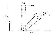
图9C说明了这一点。图9C是显示取自漏区域的电流信号(Ids)的平方根对栅108和源区域102之间建立的电压势(VGS)的曲线。
在图9C中,ΔVT表示在正常运行下由于器件的退化,产生自逐渐被陷于漏区域104附近的栅氧化110中的电子的MOSFET阈值电压的最小变化。这导致漏区域104附近的栅氧化110中固定陷阱电荷。斜率1表示图9A中没有电子陷于栅氧化110中的沟道106中的电荷载流子的迁移率。斜率2表示图9B的常规的MOSFET中有电子117陷于漏区域104附近的栅氧化110中的沟道106中的电荷载流子的迁移率。如通过图9C中斜率1和斜率2的比较所示,陷于常规的MOSFET的漏区域104附近的栅氧化110中的电子117不明显地改变沟道106中的电荷载流子的迁移率。In FIG. 9C , ΔVT represents the minimum change in MOSFET threshold voltage resulting from electrons becoming trapped in
有两个因素对受压和热电子注入的效应有关。一个因素包括由于陷阱电子引起的阈值电压的漂移,第二个因素包括由该陷阱电荷和额外的表面态引起的载流子电子的额外散射造成的迁移率退化。当常规的MOSFET在正向的运行中退化,或“受压”时,电子必将逐渐注入并陷于漏附近的栅氧化中。在常规的MOSFET的该部分中,在栅氧化下几乎没有沟道存在。这样,陷入的电荷仅稍许调整阈值电压和电荷迁移率。There are two factors related to the effect of pressurization and hot electron injection. One factor includes a shift in threshold voltage due to trapped electrons, and the second includes mobility degradation due to additional scattering of carrier electrons by this trapped charge and additional surface states. When a conventional MOSFET degrades, or "stresses," in forward operation, electrons must gradually inject and become trapped in the gate oxide near the drain. In this part of a conventional MOSFET, almost no channel exists under the gate oxide. In this way, the trapped charge adjusts threshold voltage and charge mobility only slightly.
为了形成可编程的寻址解码和纠错,本申请人以前已经叙述了可编程的存储器器件和在常规的CMOS工艺和技术中基于MOSFET的翻转受压的功能。(总体上见L.Forbes,W.P.Noble and E.H.Cloud,“MOSFET technology forprogrammable address decode and correction”,United States Patent ApplicationSerial Number 09/383,804)。但该项发明未叙述多状态存储器元件的方案,而仅是寻址解码和纠错的问题。To form programmable address decoding and error correction, the applicant has previously described programmable memory devices and MOSFET-based flip-stressed functions in conventional CMOS processes and technologies. (See generally L. Forbes, W.P. Noble and E.H. Cloud, "MOSFET technology for programmable address decode and correction", United States Patent Application Serial Number 09/383,804). However, this invention does not describe the scheme of multi-state memory elements, but only addresses decoding and error correction.
根据本发明的技术,正常的MOSFET能通过反向的运行和利用雪崩热电子注入以聚集MOSFET的栅氧化中的电子而编程。当经编程的MOSFET以后在正向运行时,陷于氧化层中的电子靠近源,并使沟道有两个不同的阈值电压区域。本发明的新颖的编程MOSFET比常规的MOSFET传导明显更小的电流,尤其在低漏电压下。除非施加负栅电压,这些电子将保留被陷于栅氧化中。当施加正栅压或零栅压时,这些电子将不从栅氧化中去除。擦除可以通过施加负栅电压或通过施加负栅偏压的同时提高温度以使陷阱电子被重新发射回MOSFET的硅沟道而完成。(总体见L.Forbes,E.Sun,R.Alders and J.Moll,“Field induced re-emission of electrons trapped in SiO2”,IEEE Trans.ElectronDevice,vol.ED-26,no.11,pp.1816-1818(Nov.1979);S.S.B.Or,N.Hwang,andL.Forbes,“Tunneling and Thermal emission from a distribution of deep traps inSiO2”,IEEE Trans.on Electron Device,Vol.40,no.6,pp.1100-1103(June1993);S.A.Abbas and R.C.Dockerty,“N-channel IGFET design limitation due tohot electron trapping”,IEEE Int.Electron Device Mtg.Washington D.C.Dec.1975,pp.35-38)。According to the technique of the present invention, normal MOSFETs can be programmed by operating in reverse and using avalanche hot electron injection to gather electrons in the MOSFET's gate oxide. When the programmed MOSFET is later operated in the forward direction, the electrons trapped in the oxide are close to the source and cause the channel to have two different threshold voltage regions. The novel programming MOSFET of the present invention conducts significantly less current than conventional MOSFETs, especially at low drain voltages. These electrons will remain trapped in the gate oxide unless a negative gate voltage is applied. These electrons will not be removed from the gate oxide when a positive or zero gate voltage is applied. Erasing can be accomplished by applying a negative gate voltage or by applying a negative gate bias while increasing the temperature so that trapped electrons are re-emitted back into the silicon channel of the MOSFET. (See generally L.Forbes, E.Sun, R.Alders and J.Moll, "Field induced re-emission of electrons trapped in SiO2 ", IEEE Trans.ElectronDevice, vol.ED-26, no.11, pp. 1816-1818 (Nov.1979); SSBOr, N.Hwang, and L.Forbes, "Tunneling and Thermal emission from a distribution of deep traps inSiO2 ", IEEE Trans.on Electron Device, Vol.40, no.6, pp .1100-1103 (June 1993); SA Abbas and RC Dockerty, "N-channel IGFET design limitation due to hot electron trapping", IEEE Int. Electron Device Mtg. Washington DC Dec. 1975, pp. 35-38).
图10A-C在说明通过反方向编程器件然后通过在正向读取该器件而获得大得多的器件性能改变的本发明中是很有用的。Figures 10A-C are useful in illustrating the present invention that a much larger change in device performance is obtained by programming a device in the reverse direction and then by reading the device in the forward direction.
图10A是可被用作根据本发明的技术的多状态元件的编程MOSFET的示意图。如图10A所示,多状态元件201包括衬底200中的MOSFET,具有第一源/漏区域202,第二源/漏区域204以及在第一和第二源/漏区域202,204之间的沟道区域206。在一个实施例中,第一源/漏区域202包括MOSFET的源区域202,第二源/漏区域204包括MOSFET的漏区域204。图10A进一步说明由栅氧化210和沟道区域206分离的栅208。第一传输线214连接到第一源/漏区域202,第二传输线连接到第二源/漏区域204。在一个实施例中,第一传输线包括源线212,第二传输线包括比特线214。10A is a schematic diagram of a programming MOSFET that can be used as a multi-state element in accordance with the techniques of the present invention. As shown in FIG. 10A , the
如上所述,多状态元件201由经编程的MOSFET构成。该编程MOSFET具有陷于和第一源/漏区域202毗邻的栅氧化210中的电荷217,因此沟道区域206在沟道206中具有第一电压阈值区域(Vt1)和第二电压阈值区域(Vt2)。在一个实施例中,陷于和第一源/漏区域202毗邻的栅氧化210中的电荷217包括俘获电子电荷217。根据本发明的原理以及下文更详尽的叙述,多状态元件可经编程而具有陷于和第一源/漏区域202毗邻的栅绝缘体中的多个电荷水平中的一个,因此沟道区域206将具有第一电压阈值区域(Vt1)和第二电压阈值区域(Vt2),这样经编程的多状态元件在经减小的源漏电流下运行。As mentioned above, the
图10A说明沟道206中的Vt2毗邻于第一源/漏区域202,沟道206中的Vt1毗邻于第二源/漏区域202。根据本发明的原理,由于陷于和第一源/漏区域202毗邻的栅氧化217的电荷217,Vt2有比Vt1更高的电压阈值。多重比特能被储存在多状态元件201上。FIG. 10A illustrates that Vt2 in the
图10B是适合于解释本发明的多状态元件201的MOSFET可以被编程而达到本发明的实施例的方法的示意图。如图10B所示,该方法包括以反方向编程MOSFET。以反方向编程MPSFET包括将第一电压势V1施加到MOSFET的漏区域204。在一个实施例中,将第一电压势V1施加到MOSFET的漏区域204包括将MOSFET的漏区域204接地,如图10B所示。第二电压势V2施加到MOSFET的源区域202。在一个实施例中,将第二电压势V2施加到源区域202包括将高正电压势(VDD)施加到MOSFET的源区域202,如图10B所示。栅电势VGS施加到MOSFET的栅208。在一个实施例中,栅电势VGS包括小于第二电压势V2,但足够建立MOSFET中漏区域204和源区域202之间的沟道206中的传导的电压势。如图10B所示,将第一,第二和栅电势(分别为V1,V2和VGS)施加到MOSFET产生了向MOSFET的和源区域202毗邻的栅氧化210注入热电子。或者说,施加第一,第二和栅电势(分别为V1,V2和VGS)向例如电子的越过沟道206传导的电荷载流子提供了足够的能量,这样,一旦电荷载流子靠近源区域202,许多的电荷载流子被激发而进入和源区域202毗邻的栅氧化210。这样,电荷载流子成为陷阱载流子。FIG. 10B is a schematic diagram suitable for explaining the method by which the MOSFETs of the
在本发明的一个实施例中,该方法由后继的读操作期间在MOSFET被编程状态中以正向运行该MOSFET而继续。因此,读操作包括将源区域202接地并预先将漏区域充电至VDD的几分之一的电压。如果器件通过连接到栅的字线被寻址,则其传导性将由在栅绝缘体中是否存在储存的电荷而确定。也就是,在和寻址和读取常规的DRAM元件一起进行的形成源漏区域之间的沟道传导的尝试中,栅电势可以通过字线216施加到栅208。In one embodiment of the invention, the method continues by operating the MOSFET in the forward direction in the MOSFET programmed state during a subsequent read operation. Thus, a read operation involves grounding the
但是,现在在其被编程的状态,MOSFET的传导沟道206将有和漏区域204毗邻的第一电压阈值区域(Vt1)以及和源区域202毗邻的第二电压阈值区域(Vt2),如结合图10A解释和叙述的一样。根据本发明的原理,由于热电子217注入MOSFET的和源区域202毗邻的栅氧化210,Vt2具有比Vt1更高的阈值电压。However, now in its programmed state, the
图10C是在第二源/漏区域204探测的电流信号(Ids)对在第二源/漏区域204和第一源/漏区域202之间建立的电压势或漏电压(VDS)(Ids对VDS)作出的曲线。在一个实施例中,VDS表示在漏区域204和源区域202之间建立的电压势。在图10C中,所作的曲线D1表示未根据本发明的原理编程的常规的MOSFET的传导行为。曲线D2表示根据本发明的原理的前文结合图10叙述的经编程的MOSFET的传导行为。如图10C所示,对于一个特定的漏电压VDS,在经编程的MOSFET的第二源漏区域204探测的电流信号(IDS2)(曲线D2)明显低于在未根据本发明的原理编程的常规的MOSFET的第二源/漏区域204探测的电流信号(IDS1)。还有,这归因于这样的事实,即在本发明的经编程的MOSFET的沟道206具有两个电压阈值区域,靠近第一源/漏区域202的电压阈值Vt2因为陷于和第一源/漏区域202毗邻的栅氧化210中的电荷217而具有比靠近第二源/漏区域的Vt1更高的电压阈值。10C is a current signal (Ids) detected in the second source/
这些效应中的一些效应近来已经被叙述用于被称为NROM的不同的器件结构作为闪存。在以色列和德国该后一项工作基于利用在非常规闪存器件结构中的氮化硅层中的电荷陷阱。(总体上见B.Eitan et al.“Characterization ofChannel Hot Electron Injection by the Subthreshold Slope of NROM Device”,IEEE Electron Device Lett.Vol.22,No.11,pp.556-558,(Nov.2001);B.Etianet al.“NROM:A Novel Localized Trapping,2-Bit Nonvolatile Memory Cell”,IEEE Electron Device Lett.Vol.21,No.11,pp.543-545,(Nov.2000)。氮化硅栅绝缘体中的电荷陷阱是在MNOS存储器器件中应用的基础机构(总体上见S.Sze,Physics of Semiconductor Devices,Wiley,N.Y.1981,pp.504-506),氧化铝栅中的电荷陷阱是在MIOS存储器器件中应用的机构(总体上见S.Sze,Physicsof Semiconductor Devices,Wiley,N.Y.1981,pp.504-506),以及本申请人以前已经揭示了在栅绝缘体中经隔离的点状缺陷处的电荷陷阱(总体上见L.Forbesand J.Geusic,“Memory Using Insulator Traps”,美国专利号6140181,公布于2000年10月31日)。Some of these effects have recently been described for a different device structure known as NROM as flash memory. This latter work in Israel and Germany is based on exploiting charge traps in silicon nitride layers in unconventional flash memory device structures. (See B. Eitan et al. "Characterization of Channel Hot Electron Injection by the Subthreshold Slope of NROM Device" in general, IEEE Electron Device Lett. Vol.22, No.11, pp.556-558, (Nov.2001); B. Etian et al. "NROM: A Novel Localized Trapping, 2-Bit Nonvolatile Memory Cell", IEEE Electron Device Lett.Vol.21, No.11, pp.543-545, (Nov.2000). Silicon nitride gate The charge trap in the insulator is the basic mechanism applied in the MNOS memory device (see generally S.Sze, Physics of Semiconductor Devices, Wiley, N.Y.1981, pp.504-506), the charge trap in the aluminum oxide gate is in the MIOS Mechanisms applied in memory devices (see generally S.Sze, Physics of Semiconductor Devices, Wiley, N.Y.1981, pp.504-506), and the applicant has previously revealed the existence of isolated point-like defects in gate insulators. Charge traps (see generally L. Forbes and J. Geusic, "Memory Using Insulator Traps", US Patent No. 6,140,181, published October 31, 2000).
和上述工作相对照,本发明揭示了以反方向编程MOSFET以靠近源区域聚集众多电荷水平中的一种水平,以及揭示了以正向读取器件以基于DRAM技术的修改形成多状态存储器元件。In contrast to the above work, the present invention discloses programming a MOSFET in the reverse direction to accumulate one of many charge levels close to the source region, and reading the device in the forward direction to form a multi-state memory element based on a modification of DRAM technology.
现有技术的DRAM技术用氧化硅作为栅绝缘体。另外,在常规的DRAM器件中的重点是尝试将氧化硅栅绝缘体中的电荷陷阱减至最小。根据本发明的原理,各种绝缘体被用于比氧化硅更高效率地聚集电子。即在本发明中,多状态存储器元件利用在诸如湿氧化硅,氮化硅,氧化氮化硅SON,富氧化硅SRO,氧化铝Al2O3,诸如先氧化硅再氮化硅,先氧化硅再氧化铝或作为氧化-氮化-氧化的多层次的这些绝缘体的复合层的栅绝缘体中的电荷陷阱。虽然氧化硅的电荷陷阱效率可能较低,但对于氮化硅或氧化辉和氮化硅的复合层而言该效率就不低。Prior art DRAM technology uses silicon oxide as the gate insulator. Additionally, in conventional DRAM devices an emphasis has been placed on trying to minimize charge traps in the silicon oxide gate insulator. In accordance with the principles of the present invention, various insulators are used to collect electrons more efficiently than silicon oxide. That is, in the present invention, multi-state memory elements are used in such as wet silicon oxide, silicon nitride, silicon oxide nitride SON, silicon-rich oxide SRO, aluminum oxide Al2 O3 , such as silicon oxide and then silicon nitride, first oxidation Charge traps in gate insulators of silicon on aluminum oxide or composite layers of these insulators as oxide-nitride-oxide multilayers. While the charge trapping efficiency of silicon oxide may be low, it is not low for silicon nitride or composite layers of oxide and silicon nitride.
图11说明了根据本发明的原理的存储器阵列300的一部分。图11中的存储器被显示为根据本发明的原理形成的许多垂直柱或多状态元件301-1和301-2。业内的熟练人士在阅读本发明的说明时将理解,该许多的垂直柱形成为从衬底303向外延伸的行和列。如图11所示,许多垂直柱301-1和301-2由许多沟槽340分离。根据本发明的原理,许多垂直柱301-1和301-2用作分别包括第一源/漏区域301-1和301-2的晶体管。第一源/漏区域301-1和301-2被连接到源线304。如图11所示,源线304形成在衬底340底部垂直柱301-1和301-2行之间。在一个实施例中,根据本发明的原理,源线304从在沟槽底部经注入的掺杂区域开始形成。分别为306-1和306-2的第二源/漏区域被连接到比特线(未显示)。沟道区域305位于第一和第二源/漏区域之间。Figure 11 illustrates a portion of a memory array 300 in accordance with the principles of the present invention. The memory in Figure 11 is shown as a number of vertical columns or multi-state elements 301-1 and 301-2 formed in accordance with the principles of the present invention. Those skilled in the art will understand upon reading the description of the present invention that the plurality of vertical columns are formed as rows and columns extending outwardly from the
如图11所示,栅309由沟槽340中沿垂直柱301-1和301-2行的栅绝缘体307和沟道区域305分离。在一个实施例中,根据本发明的原理,栅绝缘体307包括从通过湿氧化形成的二氧化硅(SiO2),氧化氮化硅(SON),富氧化硅(SRO)和氧化铝(Al2O3)的集合中选择的栅绝缘体307。在另一个实施例中,根据本发明的原理,栅绝缘体307包括从富氧化铝硅绝缘体,内含硅纳米微粒的富氧化硅,内含硅碳化物纳米微粒的氧化硅微粒的绝缘体和氧化碳化硅绝缘体的集合中选择的栅绝缘体307。在另一个实施例中,根据本发明的原理,栅绝缘体307包括复合层307。在该实施例中,复合层307包括从氧化硅-氧化铝(Al2O3)-氧化硅复合层,氧化硅-氧化碳化硅-氧化硅复合层的集合中选择的复合层307。在另一个实施例中,复合层307包括从硅(Si),钛(Ti)和钽(Ta)的集合中选择的两种或多种材料的复合层307或非化学计量的单层。在另一个实施例中,根据本发明的原理,栅绝缘体307包括氧化-氮化-氧化(ONO)栅绝缘体307。As shown in FIG. 11 ,
图12说明了图11中显示的部分存储器阵列的电等效电路400。如图12所示,设置许多垂直多状态元件401-1和401-2。每个垂直多状态元件401-1和401-2包括第一源/漏区域401-1,401-2和第二源/漏区域406-1,406-2,第一和第二源/漏区域之间的沟道区域405,和由栅绝缘体407与沟道区域分离的栅409。FIG. 12 illustrates an electrical equivalent circuit 400 of the portion of the memory array shown in FIG. 11 . As shown in FIG. 12, many vertical multi-state elements 401-1 and 401-2 are provided. Each vertical multi-state element 401-1 and 401-2 includes a first source/drain region 401-1, 401-2 and a second source/drain region 406-1, 406-2, the first and second source/drain
图12进一步说明了连接到每个多状态元件的第二源/漏区域406-1和406-2的许多比特线411-1和411-2。在一个实施例中,如图12所示,许多比特线411-1和411-2沿存储器阵列行连接到第二源/漏区域406-1和406-2。诸如图12的字线413的许多字线沿存储器阵列列连接到每个多状态元件的栅409。以及,诸如公共源线415的许多源线沿垂直多状态元件401-1和401-2列连接到例如402-1和402-2的第一源/漏区域,这样,相邻的包含这些晶体管的垂直柱就共用了共用源线415。在一个实施例中,相邻垂直柱列包括一个在共用沟槽的一侧的作为垂直多状态元件工作的例如401-1的晶体管,如结合图11叙述的分离垂直柱行的共用沟槽,和一个在共用沟槽的相对一侧的具有经编程的传导状态的作为参照元件工作的例如401-2的晶体管。在该方式中,根据本发明的原理并如下文更详尽的叙述,至少一个多状态元件可以被编程以具有以417总体显示的陷于和例如402-1的第一源/漏区域毗邻的栅绝缘体中的许多电荷水平中的一种水平,这样沟道区域405就将有第一电压阈值区域(Vt1)和第二电压阈值区域(Vt2),因此经编程的多状态元件就以经减小的源漏电流工作。FIG. 12 further illustrates a number of bit lines 411-1 and 411-2 connected to the second source/drain regions 406-1 and 406-2 of each multi-state element. In one embodiment, as shown in FIG. 12, a number of bit lines 411-1 and 411-2 are connected to second source/drain regions 406-1 and 406-2 along memory array rows. A number of word lines, such as
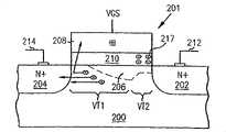
图13是在说明根据本发明的原理的新颖多状态元件500上的读操作中很有用的另一个电等效电路。图13的电等效电路描绘了一个经编程的垂直多状态元件。如结合图11的详尽解释,该经编程的垂直多状态元件500包括一个从衬底向外延伸的垂直金属氧化物半导体场效应晶体管(MOSFET)500。该MOSFET具有源区域502,漏区域506,源区域502和漏区域506之间的沟道区域505,和由以517总体显示的栅绝缘体与沟道区域505分离的栅507。FIG. 13 is another electrical equivalent circuit useful in illustrating a read operation on a novel multi-state element 500 in accordance with the principles of the present invention. The electrical equivalent circuit of Figure 13 depicts a programmed vertical multi-state element. As explained more fully in connection with FIG. 11, the programmed vertical multi-state element 500 includes a vertical metal oxide semiconductor field effect transistor (MOSFET) 500 extending outwardly from the substrate. The MOSFET has a
如图13所示,字线513连接到栅507。如结合图11叙述的形成在和垂直MOSFET毗邻的沟槽中的源线504连接到源区域502。比特线或数据线511连接到漏区域506。图13显示的多状态元件500是具有如以517总体显示的陷于和第一源/漏区域502毗邻的栅绝缘体中的许多电荷水平中的一个水平的经编程的多状态元件500的一个实例,这样沟道区域405就将有第一电压阈值区域(Vt1)和第二电压阈值区域(Vt2),因此经编程的多状态元件500就以经减小的源漏电流工作。根据本发明的原理,第二电压阈值区域(Vt2)现在是一个大于第一电压阈值区域(Vt1)的高电压阈值区域。
图14说明了根据本发明的原理的存储器阵列600的一部分。图14的存储器被显示为描绘一对根据本发明的原理形成的多状态元件601-1和601-2。通过阅读本发明的说明,业内的普通熟练人士将理解,在一个阵列中可以组织任何数量的多状态元件,但图14中的显示仅说明两个元件的情况。如图14所示,第一源/漏区域602-1和602-2分别连接到源线604。第二源/漏区域606-1和606-2分别连接到比特线608-1和608-2。每一条比特线608-1和608-2都连接到以610总体显示的传感放大器。字线612-1和612-2分别连接到每一个多状态元件601-1和601-2的栅614-1和614-2。根据本发明的原理,字线612-1和612-2的走向横越或垂直于存储器阵列600的行。最后,以624显示的写数据/预充电电路用于将第一或第二电势连接到比特线608-1。通过阅读本发明的说明,业内的普通熟练人士将理解,写数据/预充电电路624适合于在反向的写操作期间将地连接到比特线608-1,或在正向的读操作期间将比特线608-1预充电到VDD电压的几分之一。通过阅读本发明的说明,业内的普通熟练人士将理解,在反向的写操作期间源线604可以加上大于VDD电压的偏压,或者在正向的读操作中接地。Figure 14 illustrates a portion of a
如图14所示,包括多状态元件601-1和601-2的阵列结构600没有电容器。作为替代,根据本发明的原理,第一源/漏区域或源区域602-1和602-2直接连接到源线604。为了写操作,源线604被加以高于VDD电压的偏压,器件因将数据或比特线608-1或608-2接地而在反向受压。如果多状态元件601-1或601-2通过字线寻址612-1和612-2被选中,则多状态元件601-1或601-2将进行伴随的热电子注入并因此而受压,热电子被注入到和源区域602-1或602-2毗邻的元件栅绝缘体中。通过阅读本发明的说明,业内的普通熟练人士将理解,许多不同的电荷水平可以经编程而进入和源区域毗邻的栅绝缘体,这样,该元件被用作差动元件和/或该元件被和一个参照的或虚设的元件比较,如图14所示,多重比特就可以储存在多状态元件上。As shown in FIG. 14,
在读多状态元件期间,601-1或601-2以正向运行,源线604接地,比特线608-1或608-2和元件的各个第二源/漏区域或漏区域606-1和606-2被预充电到Vdd电压的几分之一。如果器件由字线612-1或612-2寻址,则其传导性将由陷于栅绝缘体中的所储存的电荷数量是否存在而确定,该陷于栅绝缘体中的电荷数量被测量或和参照或虚设元件比较,而用传感放大器610探测。例如,在授予Micron Technology Inc.的美国专利5627785,5280205和5042011号中叙述了DRAM传感放大器的操作,这些专利通过引用而结合在本文中。阵列将这样以DRAM中应用的常规方式寻址和读取,但以新颖的方式作为多状态元件编程。During a read of a multi-state element, 601-1 or 601-2 operates in the forward direction,
在运行中,器件将因在源线604加以偏压而在反向经受热电子的压力,而在读器件时将源线604接地以将例如元件601-1的受压的多状态元件和例如601-2的非受压的虚设器件/元件比较,如图14所示。可以在制造和试验期间应用写和可能的擦除特征以在最初将所有元件或器件在电场中使用之前编程到使其具有相似或相匹配的传导性。同样,在例如601-2的参照或虚设元件中的晶体管也可以最初被全部编程到使其具有同样的传导状态。根据本发明的原理,然后传感放大器610可以探测元件或器件性能中由于写操作期间器件性能上的受压诱导的改变引起的微小差别。In operation, the device will experience hot electron stress in the reverse direction by biasing
通过阅读本发明的说明,业内的普通熟练人士将理解,这样的多状态元件的阵列方便地通过修改DRAM技术而实现。根据本发明的原理,多状态元件的栅绝缘体包括从通过湿氧化形成的厚SiO2层,SON氧化氮化硅,SRO富氧化硅,Al2O3氧化铝,复合层和带有陷阱的经注入的氧化物(L.Forbes and J.Geusic,“Memory Using Insulators Traps”,公布于2000年10月31日的美国专利1640181号)的集合中选择的栅绝缘体。用于寻址解码和传感放大器的常规的晶体管可以在氧化硅的正常薄栅绝缘体的步骤之后制造。Those of ordinary skill in the art will appreciate, upon reading the description of the present invention, that such arrays of multi-state elements are conveniently implemented by modifying DRAM technology. According to the principles of the present invention, the gate insulator of a multi-state element consists of thickSiO2 layer formed by wet oxidation, SON oxide silicon nitride, SRO rich silicon oxide,Al2O3 aluminum oxide, compositelayer and via Gate insulators of choice from the collection of implanted oxides (L. Forbes and J. Geusic, "Memory Using Insulators Traps," US Patent No. 1,640,181, published October 31, 2000). Conventional transistors for address decoding and sense amplifiers can be fabricated after the normal thin gate insulator step of silicon oxide.
图15A-15B和图16A-16B在说明根据本发明的原理用栅绝缘体中的电荷储存调整多状态元件的传导性中是很有用的。也就是,图15A-16B说明了根据本发明的原理形成的新颖多状态元件701的运行。如图15A所示,栅绝缘体707有若干层次,例如一个ONO堆,其中层707A是最靠近沟道705的氧化层,氮化层707B形成在其上。在图15A显示的实施例中,氧化层707A被显示为具有约6.7nm或


图15B有助于进一步说明本发明的新颖多状态元件的传导行为。图15B显示的电等效电路显示了一个具有
图16A和16B说明了如上所述的新颖多状态元件的运行和编程。但是,图16A和16B也有助于说明一种替代的阵列设计,其中相邻的器件被进行比较,共用沟槽的相对侧上的一个器件被用作虚设元件晶体管或参照器件。还有,参照器件可以全部被编程使其具有相同的初始传导状态。图16A说明了新颖的多状态元件反向的运行和编程。如图16A所示,在沟槽的一侧的晶体管801-1(如结合图11所述)因其各个漏线例如811-1的接地而受压。如图16A所示,在沟槽的相对侧上的晶体管801-2的漏线811-2处于浮动状态。电压被施加到现在被用作漏的位于沟槽底部共用的源线804(如结合图11所述)。如该电等效电路所示,相邻的(共用沟槽)/列相邻晶体管801-1和801-2共用栅807,连接到其上的例如多晶硅栅线的字线813的走向横越或垂直于包含例如811-1,811-2和804的比特线和源线的行。栅电压被施加到栅807。这里,多状态元件801-1将进行伴随的热电子注入并因此受压,热电子被注入和源区域802-1毗邻的元件栅绝缘体817。Figures 16A and 16B illustrate the operation and programming of the novel multi-state element as described above. However, Figures 16A and 16B also help illustrate an alternative array design in which adjacent devices are compared and one device on the opposite side of the shared trench is used as a dummy element transistor or reference device. Also, the reference devices can all be programmed to have the same initial conduction state. Figure 16A illustrates the operation and programming of the novel multi-state element inverse. As shown in FIG. 16A, transistor 801-1 on one side of the trench (as described in connection with FIG. 11) is stressed by its respective drain line, eg, 811-1, to ground. As shown in FIG. 16A, the drain line 811-2 of the transistor 801-2 on the opposite side of the trench is in a floating state. The voltage is applied to the common source line 804 (as described in connection with FIG. 11 ) at the bottom of the trenches which is now used as a drain. As shown in this electrical equivalent circuit, adjacent (shared trench)/column adjacent transistors 801-1 and 801-2 share a
图16B显示在经如此编程的多状态元件在正向的运行以及在例如每个元件有两个晶体管的差动元件实施例中发生的差动读出。为了读该状态,漏和源(或地)有正常的连接并确定多状态元件的传导性。也就是,漏线811-1和811-2有施加到其上的正常的正向电势。位于沟槽底部的共用源线804(如结合图11所述)接地并再次被用作源。以及,栅电压被施加到栅807。通过阅读本发明的说明,业内的普通熟练人士将理解,许多不同的电荷水平可以被编程进入和源区域802-1毗邻的栅绝缘体817并和参照元件或虚设元件802-2比较。这样,根据本发明的原理,多重比特可以储存在多状态元件上。Figure 16B shows differential sensing occurring in the forward direction of a multi-state cell thus programmed and in an embodiment of a differential cell such as two transistors per cell. To read the state, drain and source (or ground) are normally connected and determine the conductivity of the multi-state element. That is, the drain lines 811-1 and 811-2 have normal forward potentials applied thereto. A common source line 804 (as described in connection with FIG. 11 ) at the bottom of the trench is grounded and used again as a source. And, a gate voltage is applied to the
如上所述,这些新颖的多状态元件可以用于DRAM一类的阵列中。当从上看时,两个晶体管可占据4F平方的面积(F=最小光刻特征尺寸),或由一个晶体管构成的每个存储器元件利用了2F平方的面积。但现在每个晶体管存储很多比特,因此数据存储密度大大高于每1F平方单位面积1比特。用每个存储器晶体管的参照或虚设元件,其中参照晶体管紧密相邻,例如图16A和16B所示的实施例和图12显示的实施例相对,导致晶体管的更好的匹配特性,但是有更低的存储器密度。As noted above, these novel multi-state elements can be used in DRAM-like arrays. When viewed from above, two transistors may occupy an area of 4F square (F=minimum lithographic feature size), or each memory element made up of one transistor utilizes an area of 2F square. But now each transistor stores many bits, so the data storage density is much higher than 1 bit per 1F square unit area. Using a reference or dummy element for each memory transistor, where the reference transistors are in close proximity, such as the embodiment shown in Figures 16A and 16B as opposed to the embodiment shown in Figure 12, results in better matching characteristics of the transistors, but with lower memory density.
在图17中根据本发明的原理说明了存储器器件。存储器器件940包含存储器阵列942,行和列解码器944,948和传感放大器电路946。存储器阵列942由根据本发明的原理形成的众多多状态元件900构成,其字线980和比特线960分别被共同排列成行和列。存储器阵列942的比特线960连接到传感放大器电路946,同时其字线980连接到行解码器944。寻址和控制信号在寻址/控制线961上输入到存储器器件940中并连接到列解码器948,传感放大器电路946和行解码器944,并除了其他功能外还被用于获得向存储器阵列942的读写访问。A memory device is illustrated in FIG. 17 in accordance with the principles of the present invention. The
列解码器948通过在列选择线962上的控制和列选择信号连接到传感放大器电路946。传感放大器电路946接收为存储器阵列942指定的输入数据并将从存储器阵列942读取的数据输出到输入/输出(I/O)数据线963上。通过激励字线980(通过行解码器944)从存储器阵列942的元件读取数据,字线980将所有相应于该字线的存储器元件连接到各个比特线960,比特线960限定了阵列的列。也激励了一个或多个比特线960。当一个具体的字线980和比特线960被激励时,连接到比特线列的传感放大器电路946探测和放大通过给出的多状态元件检测的传导信号,其中在读操作中,给出元件的源区域连接到接地的阵列板(未显示),并通过测量经激励的比特线960和可以是未激励的比特线但是参照线之间的电势差转移到其比特线960。存储器器件传感放大器的操作在例如美国专利5627785,5280205和5042011中叙述,这些专利都被转让于Micron Technology Inc.并通过引用而结合在本文中。
图18为利用根据本发明构成的多状态存储器元件1012的电系统或处理器基系统1000的框图。即多状态存储器元件1012利用如结合图2-4详尽解释和叙述的经修改的DRAM元件。处理器基系统1000可以是一个计算机系统,处理控制系统或任何其他应用处理器和相关存储器的系统。系统1000包括一个例如微处理器的在总线1020上和多状态存储器1012和I/O装置1008联通的中心处理单元(CPU)1002。必须指出总线1020可以是一系列在处理器基系统中普遍使用的总线和桥路,但仅为方便的目的,总线1020被显示为一根单总线。图中显示了第二I/O装置1010,但对于实施本发明是不必要的。处理器基系统1000也可以包括只读存储器(ROM)1014以及可以包括外围装置,诸如软盘驱动器1004和光盘(CD)ROM驱动器1006,在技术上众所周知,这些装置都在总线1020上和CPU 1002联通。18 is a block diagram of an electrical or processor-based
业内的熟练人士将理解,可以设置附加的电路和控制信号,存储器装置1000已经被简化以有助于突出本发明。至少一个NROM 1012中的多状态元件包括一个具有陷于和第一源/漏区域或源区域毗邻的栅绝缘体中的电荷的经编程的MOSFET,这样沟道区域具有第一电压阈值区域(Vt1)和第二电压阈值区域(Vt2),其中Vt2大于Vt1,并且Vt2和源区域毗邻,因此经编程的MOSFET在减小的源漏电流下工作。Those skilled in the art will appreciate that additional circuitry and control signals may be provided, and that
可以理解,图18显示的实施例说明了一个用于电子系统电路的实施例,其中应用了本发明的新颖的存储器元件。图18显示的对系统1000的说明旨在对于本发明的结构和电路的一种应用提供总体的理解,并不是作为对应用该新颖存储器元件结构的电子系统的元件和特征的全面的叙述。另外,本发明同样可应用于任何尺寸和类型的使用本发明的新颖存储器元件的存储器装置1000,并不限于上文的叙述。业内的普通熟练人士将理解,为了减少处理器和存储器装置之间的联通时间,这样的电子系统可以在单封装的处理单元中制造,或甚至可以在单半导体芯片上制造。It will be appreciated that the embodiment shown in Figure 18 illustrates an embodiment for use in an electronic system circuit in which the novel memory element of the present invention is employed. The illustration of
包含如本说明书中叙述的本发明的新颖存储器元件的各种应用包括在存储器模块,器件驱动器,功率模块,通讯调制解调器,处理器模块以及特殊应用模块中使用的电子系统,以及可以包括多层次多芯片的模块。这样的电路可以进一步为诸如时钟,电视,移动电话,个人计算机,汽车,工业控制系统,飞行器或其他的各种电子系统的次级元件。Various applications incorporating the novel memory elements of the present invention as described in this specification include electronic systems used in memory modules, device drivers, power modules, communication modems, processor modules, and application-specific modules, and may include multiple levels of Chip modules. Such circuits may further be secondary components of various electronic systems such as clocks, televisions, mobile phones, personal computers, automobiles, industrial control systems, aircraft or others.
结论in conclusion
对于良好建立的DRAM技术和阵列的修改的应用将被用以提供非昂贵的存储器装置,如果信息在以后被转移到其他的媒介,例如CDROM上,这样的存储器装置可以被认为是一次性的。DRAM阵列结构的高密度将以每比特非常低成本地提供对许多数字数据或图象数据的储存。可以有很多各种应用,其中数据仅需被写有限次数,这些存储器的低成本将使其更有效率地正好利用新的存储器阵列以及处置老的存储器阵列,而不是如用电流闪存进行的工作那样试图擦除和重新利用这些阵列。新颖的多状态元件可以被用于DRAM类的阵列。当从上看时,两个晶体管可以占据4F平方的面积(F=最小光刻特征尺寸),或由一个晶体管构成的每个存储器元件利用2F平方的面积。但现在每个这样的晶体管可以储存很多比特,因此数据存储密度大大高于每1F平方单位面积的1比特。应用每个存储器晶体管的参照或虚设元件,其中参照晶体管紧密相邻,例如图16A和16B所示的实施例和图12显示的实施例相对,导致晶体管的更好的匹配特性,但是有更低的存储器密度。Modifications to well-established DRAM technology and arrays will be used to provide inexpensive memory devices that can be considered disposable if the information is later transferred to other media, such as CDROM. The high density of the DRAM array structure will provide storage of large amounts of digital or image data at very low cost per bit. There can be a wide variety of applications where data only needs to be written a limited number of times and the low cost of these memories will make it more efficient to just utilize new memory arrays as well as dispose of old ones, rather than working like current flash memory That attempts to erase and repurpose these arrays. The novel multi-state elements can be used in DRAM-like arrays. When viewed from above, two transistors can occupy an area of 4F square (F = minimum lithographic feature size), or each memory element made of one transistor utilizes an area of 2F square. But now each such transistor can store many bits, so the data storage density is much higher than 1 bit per 1F square unit area. Applying a reference or dummy element for each memory transistor, where the reference transistors are in close proximity, such as the embodiment shown in Figures 16A and 16B as opposed to the embodiment shown in Figure 12, results in better matching characteristics of the transistors, but with lower memory density.
应该理解,上文的叙述只是说明性的而不是限制性的。通过阅读上文的叙述,很多其他的实施例对于业内的熟练人士是显而易见的。因此本发明的范围将参照附后的权利要求以及这样的权利要求据以建立的等效物的全部范围而确定。It should be understood that the foregoing description is illustrative only and not restrictive. Many other embodiments will be apparent to those skilled in the art from reading the above description. The scope of the invention is therefore to be determined with reference to the appended claims, along with the full scope of equivalents to which such claims are entitled.
Claims (108)
Translated fromChineseApplications Claiming Priority (4)
| Application Number | Priority Date | Filing Date | Title |
|---|---|---|---|
| US10/177,211 | 2002-06-21 | ||
| US10/177,211US20030235076A1 (en) | 2002-06-21 | 2002-06-21 | Multistate NROM having a storage density much greater than 1 Bit per 1F2 |
| US10/232,411US20040041214A1 (en) | 2002-08-29 | 2002-08-29 | One F2 memory cell, memory array, related devices and methods |
| US10/232,411 | 2002-08-29 |
Publications (2)
| Publication Number | Publication Date |
|---|---|
| CN1675770A CN1675770A (en) | 2005-09-28 |
| CN100407427Ctrue CN100407427C (en) | 2008-07-30 |
Family
ID=30002651
Family Applications (1)
| Application Number | Title | Priority Date | Filing Date |
|---|---|---|---|
| CN038196913AExpired - LifetimeCN100407427C (en) | 2002-06-21 | 2003-06-19 | NROM memory element, memory array, related apparatus and method |
Country Status (8)
| Country | Link |
|---|---|
| US (3) | US7220634B2 (en) |
| EP (1) | EP1530803A2 (en) |
| JP (2) | JP4678760B2 (en) |
| KR (1) | KR100864135B1 (en) |
| CN (1) | CN100407427C (en) |
| AU (1) | AU2003263748A1 (en) |
| SG (1) | SG125143A1 (en) |
| WO (1) | WO2004001802A2 (en) |
Cited By (1)
| Publication number | Priority date | Publication date | Assignee | Title |
|---|---|---|---|---|
| CN104969358A (en)* | 2013-03-14 | 2015-10-07 | 硅存储技术公司 | Nonvolatile memory cells and arrays with charge trapping layers in trenches and method of manufacturing same |
Families Citing this family (138)
| Publication number | Priority date | Publication date | Assignee | Title |
|---|---|---|---|---|
| US20040041214A1 (en)* | 2002-08-29 | 2004-03-04 | Prall Kirk D. | One F2 memory cell, memory array, related devices and methods |
| JP4334315B2 (en)* | 2003-10-10 | 2009-09-30 | 株式会社ルネサステクノロジ | Manufacturing method of semiconductor memory device |
| US7050330B2 (en) | 2003-12-16 | 2006-05-23 | Micron Technology, Inc. | Multi-state NROM device |
| TWI251337B (en)* | 2003-12-29 | 2006-03-11 | Powerchip Semiconductor Corp | Non-volatile memory cell and manufacturing method thereof |
| KR100546409B1 (en)* | 2004-05-11 | 2006-01-26 | 삼성전자주식회사 | 2-bit sonos-type memory cell with recess channel and method of manufacturing the same |
| DE102004028679A1 (en)* | 2004-06-14 | 2006-01-05 | Infineon Technologies Ag | Isolation grave arrangement |
| US7190616B2 (en)* | 2004-07-19 | 2007-03-13 | Micron Technology, Inc. | In-service reconfigurable DRAM and flash memory device |
| US7271052B1 (en)* | 2004-09-02 | 2007-09-18 | Micron Technology, Inc. | Long retention time single transistor vertical memory gain cell |
| KR100634266B1 (en)* | 2004-09-02 | 2006-10-13 | 삼성전자주식회사 | Nonvolatile memory device, method for manufacturing same and method for operating same |
| US7053447B2 (en)* | 2004-09-14 | 2006-05-30 | Infineon Technologies Ag | Charge-trapping semiconductor memory device |
| TWI253748B (en)* | 2004-09-17 | 2006-04-21 | Powerchip Semiconductor Corp | Nonvolatile memory and manufacturing method and operating method thereof |
| US7518179B2 (en) | 2004-10-08 | 2009-04-14 | Freescale Semiconductor, Inc. | Virtual ground memory array and method therefor |
| KR100630725B1 (en)* | 2004-12-17 | 2006-10-02 | 삼성전자주식회사 | Semiconductor device having buried bit line and manufacturing method thereof |
| US7365382B2 (en)* | 2005-02-28 | 2008-04-29 | Infineon Technologies Ag | Semiconductor memory having charge trapping memory cells and fabrication method thereof |
| US7619275B2 (en) | 2005-07-25 | 2009-11-17 | Freescale Semiconductor, Inc. | Process for forming an electronic device including discontinuous storage elements |
| US7582929B2 (en) | 2005-07-25 | 2009-09-01 | Freescale Semiconductor, Inc | Electronic device including discontinuous storage elements |
| US20070020840A1 (en)* | 2005-07-25 | 2007-01-25 | Freescale Semiconductor, Inc. | Programmable structure including nanocrystal storage elements in a trench |
| US7262997B2 (en)* | 2005-07-25 | 2007-08-28 | Freescale Semiconductor, Inc. | Process for operating an electronic device including a memory array and conductive lines |
| US7394686B2 (en)* | 2005-07-25 | 2008-07-01 | Freescale Semiconductor, Inc. | Programmable structure including discontinuous storage elements and spacer control gates in a trench |
| US7619270B2 (en) | 2005-07-25 | 2009-11-17 | Freescale Semiconductor, Inc. | Electronic device including discontinuous storage elements |
| US7112490B1 (en)* | 2005-07-25 | 2006-09-26 | Freescale Semiconductor, Inc. | Hot carrier injection programmable structure including discontinuous storage elements and spacer control gates in a trench |
| US7256454B2 (en)* | 2005-07-25 | 2007-08-14 | Freescale Semiconductor, Inc | Electronic device including discontinuous storage elements and a process for forming the same |
| US7314798B2 (en)* | 2005-07-25 | 2008-01-01 | Freescale Semiconductor, Inc. | Method of fabricating a nonvolatile storage array with continuous control gate employing hot carrier injection programming |
| US7642594B2 (en) | 2005-07-25 | 2010-01-05 | Freescale Semiconductor, Inc | Electronic device including gate lines, bit lines, or a combination thereof |
| US7250340B2 (en)* | 2005-07-25 | 2007-07-31 | Freescale Semiconductor, Inc. | Method of fabricating programmable structure including discontinuous storage elements and spacer control gates in a trench |
| US7285819B2 (en)* | 2005-07-25 | 2007-10-23 | Freescale Semiconductor, Inc. | Nonvolatile storage array with continuous control gate employing hot carrier injection programming |
| US7592224B2 (en) | 2006-03-30 | 2009-09-22 | Freescale Semiconductor, Inc | Method of fabricating a storage device including decontinuous storage elements within and between trenches |
| KR100777016B1 (en) | 2006-06-20 | 2007-11-16 | 재단법인서울대학교산학협력재단 | NAND flash memory array with columnar structure and manufacturing method |
| US7906804B2 (en)* | 2006-07-19 | 2011-03-15 | Kabushiki Kaisha Toshiba | Nonvolatile semiconductor memory device and manufacturing method thereof |
| US7785965B2 (en)* | 2006-09-08 | 2010-08-31 | Spansion Llc | Dual storage node memory devices and methods for fabricating the same |
| WO2008036552A2 (en)* | 2006-09-19 | 2008-03-27 | Sandisk Corporation | Array of non-volatile memory cells with floating gates formed of spacers in substrate trenches |
| US7838920B2 (en)* | 2006-12-04 | 2010-11-23 | Micron Technology, Inc. | Trench memory structures and operation |
| JP2008166528A (en)* | 2006-12-28 | 2008-07-17 | Spansion Llc | Semiconductor device and manufacturing method thereof |
| US7651916B2 (en)* | 2007-01-24 | 2010-01-26 | Freescale Semiconductor, Inc | Electronic device including trenches and discontinuous storage elements and processes of forming and using the same |
| US7572699B2 (en) | 2007-01-24 | 2009-08-11 | Freescale Semiconductor, Inc | Process of forming an electronic device including fins and discontinuous storage elements |
| US7838922B2 (en) | 2007-01-24 | 2010-11-23 | Freescale Semiconductor, Inc. | Electronic device including trenches and discontinuous storage elements |
| JP5301123B2 (en) | 2007-07-25 | 2013-09-25 | スパンション エルエルシー | Semiconductor device and manufacturing method thereof |
| US8320191B2 (en) | 2007-08-30 | 2012-11-27 | Infineon Technologies Ag | Memory cell arrangement, method for controlling a memory cell, memory array and electronic device |
| US8365040B2 (en) | 2007-09-20 | 2013-01-29 | Densbits Technologies Ltd. | Systems and methods for handling immediate data errors in flash memory |
| US8650352B2 (en)* | 2007-09-20 | 2014-02-11 | Densbits Technologies Ltd. | Systems and methods for determining logical values of coupled flash memory cells |
| US8694715B2 (en) | 2007-10-22 | 2014-04-08 | Densbits Technologies Ltd. | Methods for adaptively programming flash memory devices and flash memory systems incorporating same |
| US8443242B2 (en) | 2007-10-25 | 2013-05-14 | Densbits Technologies Ltd. | Systems and methods for multiple coding rates in flash devices |
| WO2009072105A2 (en)* | 2007-12-05 | 2009-06-11 | Densbits Technologies Ltd. | A low power chien-search based bch/rs decoding system for flash memory, mobile communications devices and other applications |
| US8335977B2 (en) | 2007-12-05 | 2012-12-18 | Densbits Technologies Ltd. | Flash memory apparatus and methods using a plurality of decoding stages including optional use of concatenated BCH codes and/or designation of “first below” cells |
| US8321625B2 (en) | 2007-12-05 | 2012-11-27 | Densbits Technologies Ltd. | Flash memory device with physical cell value deterioration accommodation and methods useful in conjunction therewith |
| US8359516B2 (en) | 2007-12-12 | 2013-01-22 | Densbits Technologies Ltd. | Systems and methods for error correction and decoding on multi-level physical media |
| US8276051B2 (en) | 2007-12-12 | 2012-09-25 | Densbits Technologies Ltd. | Chien-search system employing a clock-gating scheme to save power for error correction decoder and other applications |
| US8327246B2 (en) | 2007-12-18 | 2012-12-04 | Densbits Technologies Ltd. | Apparatus for coding at a plurality of rates in multi-level flash memory systems, and methods useful in conjunction therewith |
| US8710576B2 (en)* | 2008-02-12 | 2014-04-29 | Halo Lsi Inc. | High density vertical structure nitride flash memory |
| WO2009118720A2 (en)* | 2008-03-25 | 2009-10-01 | Densbits Technologies Ltd. | Apparatus and methods for hardware-efficient unbiased rounding |
| JP2010003916A (en)* | 2008-06-20 | 2010-01-07 | Elpida Memory Inc | Semiconductor device and method of manufacturing the same |
| US8332725B2 (en) | 2008-08-20 | 2012-12-11 | Densbits Technologies Ltd. | Reprogramming non volatile memory portions |
| KR101529575B1 (en)* | 2008-09-10 | 2015-06-29 | 삼성전자주식회사 | Transistor, inverter comprising the same and methods of manufacturing transistor and inverter |
| KR101517390B1 (en)* | 2008-11-03 | 2015-05-04 | 삼성전자주식회사 | Vertical type semiconductor device and method for manufacturing the same |
| US8819385B2 (en) | 2009-04-06 | 2014-08-26 | Densbits Technologies Ltd. | Device and method for managing a flash memory |
| US8458574B2 (en) | 2009-04-06 | 2013-06-04 | Densbits Technologies Ltd. | Compact chien-search based decoding apparatus and method |
| US8566510B2 (en) | 2009-05-12 | 2013-10-22 | Densbits Technologies Ltd. | Systems and method for flash memory management |
| US8305812B2 (en)* | 2009-08-26 | 2012-11-06 | Densbits Technologies Ltd. | Flash memory module and method for programming a page of flash memory cells |
| US8995197B1 (en) | 2009-08-26 | 2015-03-31 | Densbits Technologies Ltd. | System and methods for dynamic erase and program control for flash memory device memories |
| US8868821B2 (en) | 2009-08-26 | 2014-10-21 | Densbits Technologies Ltd. | Systems and methods for pre-equalization and code design for a flash memory |
| US9330767B1 (en) | 2009-08-26 | 2016-05-03 | Avago Technologies General Ip (Singapore) Pte. Ltd. | Flash memory module and method for programming a page of flash memory cells |
| US8730729B2 (en) | 2009-10-15 | 2014-05-20 | Densbits Technologies Ltd. | Systems and methods for averaging error rates in non-volatile devices and storage systems |
| US8724387B2 (en) | 2009-10-22 | 2014-05-13 | Densbits Technologies Ltd. | Method, system, and computer readable medium for reading and programming flash memory cells using multiple bias voltages |
| US8626988B2 (en)* | 2009-11-19 | 2014-01-07 | Densbits Technologies Ltd. | System and method for uncoded bit error rate equalization via interleaving |
| US9037777B2 (en)* | 2009-12-22 | 2015-05-19 | Densbits Technologies Ltd. | Device, system, and method for reducing program/read disturb in flash arrays |
| US8508997B2 (en) | 2009-12-23 | 2013-08-13 | Intel Corporation | Multi-cell vertical memory nodes |
| US8222140B2 (en)* | 2009-12-23 | 2012-07-17 | Intel Corporation | Pitch division patterning techniques |
| US8607124B2 (en)* | 2009-12-24 | 2013-12-10 | Densbits Technologies Ltd. | System and method for setting a flash memory cell read threshold |
| US8885407B1 (en)* | 2010-01-19 | 2014-11-11 | Perumal Ratnam | Vertical memory cells and methods, architectures and devices for the same |
| KR20110085179A (en)* | 2010-01-19 | 2011-07-27 | 주식회사 하이닉스반도체 | Semiconductor memory device and manufacturing method thereof |
| US8341502B2 (en)* | 2010-02-28 | 2012-12-25 | Densbits Technologies Ltd. | System and method for multi-dimensional decoding |
| US8516274B2 (en) | 2010-04-06 | 2013-08-20 | Densbits Technologies Ltd. | Method, system and medium for analog encryption in a flash memory |
| US8527840B2 (en) | 2010-04-06 | 2013-09-03 | Densbits Technologies Ltd. | System and method for restoring damaged data programmed on a flash device |
| US8745317B2 (en) | 2010-04-07 | 2014-06-03 | Densbits Technologies Ltd. | System and method for storing information in a multi-level cell memory |
| CN102222524B (en)* | 2010-04-14 | 2014-07-16 | 旺宏电子股份有限公司 | Method for operating memory cell |
| CN101847655B (en)* | 2010-04-22 | 2014-10-22 | 上海华虹宏力半导体制造有限公司 | Trench grate capable of improving trench grate MOS device performance and manufacture method thereof |
| US9021177B2 (en) | 2010-04-29 | 2015-04-28 | Densbits Technologies Ltd. | System and method for allocating and using spare blocks in a flash memory |
| TWI426600B (en)* | 2010-05-13 | 2014-02-11 | Macronix Int Co Ltd | Method of operating memory cell |
| US8535992B2 (en) | 2010-06-29 | 2013-09-17 | Micron Technology, Inc. | Thyristor random access memory device and method |
| US8539311B2 (en) | 2010-07-01 | 2013-09-17 | Densbits Technologies Ltd. | System and method for data recovery in multi-level cell memories |
| US8468431B2 (en) | 2010-07-01 | 2013-06-18 | Densbits Technologies Ltd. | System and method for multi-dimensional encoding and decoding |
| US20120008414A1 (en) | 2010-07-06 | 2012-01-12 | Michael Katz | Systems and methods for storing, retrieving, and adjusting read thresholds in flash memory storage system |
| US20120019284A1 (en)* | 2010-07-26 | 2012-01-26 | Infineon Technologies Austria Ag | Normally-Off Field Effect Transistor, a Manufacturing Method Therefor and a Method for Programming a Power Field Effect Transistor |
| US8964464B2 (en) | 2010-08-24 | 2015-02-24 | Densbits Technologies Ltd. | System and method for accelerated sampling |
| US8508995B2 (en) | 2010-09-15 | 2013-08-13 | Densbits Technologies Ltd. | System and method for adjusting read voltage thresholds in memories |
| US9063878B2 (en) | 2010-11-03 | 2015-06-23 | Densbits Technologies Ltd. | Method, system and computer readable medium for copy back |
| TWI427775B (en)* | 2010-11-25 | 2014-02-21 | Macronix Int Co Ltd | Semiconductor integrated circuit device and method of manufacturing a semiconductor integrated circuit device |
| US8850100B2 (en) | 2010-12-07 | 2014-09-30 | Densbits Technologies Ltd. | Interleaving codeword portions between multiple planes and/or dies of a flash memory device |
| US10079068B2 (en) | 2011-02-23 | 2018-09-18 | Avago Technologies General Ip (Singapore) Pte. Ltd. | Devices and method for wear estimation based memory management |
| US8693258B2 (en) | 2011-03-17 | 2014-04-08 | Densbits Technologies Ltd. | Obtaining soft information using a hard interface |
| US8990665B1 (en) | 2011-04-06 | 2015-03-24 | Densbits Technologies Ltd. | System, method and computer program product for joint search of a read threshold and soft decoding |
| KR20120117127A (en)* | 2011-04-14 | 2012-10-24 | 삼성전자주식회사 | A shallow trench isolation layer structure and method for forming the same |
| US9195592B1 (en) | 2011-05-12 | 2015-11-24 | Densbits Technologies Ltd. | Advanced management of a non-volatile memory |
| US9396106B2 (en) | 2011-05-12 | 2016-07-19 | Avago Technologies General Ip (Singapore) Pte. Ltd. | Advanced management of a non-volatile memory |
| US9372792B1 (en) | 2011-05-12 | 2016-06-21 | Avago Technologies General Ip (Singapore) Pte. Ltd. | Advanced management of a non-volatile memory |
| US9110785B1 (en) | 2011-05-12 | 2015-08-18 | Densbits Technologies Ltd. | Ordered merge of data sectors that belong to memory space portions |
| US8996790B1 (en) | 2011-05-12 | 2015-03-31 | Densbits Technologies Ltd. | System and method for flash memory management |
| US9501392B1 (en) | 2011-05-12 | 2016-11-22 | Avago Technologies General Ip (Singapore) Pte. Ltd. | Management of a non-volatile memory module |
| US8667211B2 (en) | 2011-06-01 | 2014-03-04 | Densbits Technologies Ltd. | System and method for managing a non-volatile memory |
| US8588003B1 (en) | 2011-08-01 | 2013-11-19 | Densbits Technologies Ltd. | System, method and computer program product for programming and for recovering from a power failure |
| US8553468B2 (en) | 2011-09-21 | 2013-10-08 | Densbits Technologies Ltd. | System and method for managing erase operations in a non-volatile memory |
| US8996788B2 (en) | 2012-02-09 | 2015-03-31 | Densbits Technologies Ltd. | Configurable flash interface |
| US8947941B2 (en) | 2012-02-09 | 2015-02-03 | Densbits Technologies Ltd. | State responsive operations relating to flash memory cells |
| US8575035B2 (en)* | 2012-02-22 | 2013-11-05 | Omnivision Technologies, Inc. | Methods of forming varying depth trenches in semiconductor devices |
| US8996793B1 (en) | 2012-04-24 | 2015-03-31 | Densbits Technologies Ltd. | System, method and computer readable medium for generating soft information |
| US8838937B1 (en) | 2012-05-23 | 2014-09-16 | Densbits Technologies Ltd. | Methods, systems and computer readable medium for writing and reading data |
| US8879325B1 (en) | 2012-05-30 | 2014-11-04 | Densbits Technologies Ltd. | System, method and computer program product for processing read threshold information and for reading a flash memory module |
| US9921954B1 (en) | 2012-08-27 | 2018-03-20 | Avago Technologies General Ip (Singapore) Pte. Ltd. | Method and system for split flash memory management between host and storage controller |
| US8796751B2 (en)* | 2012-11-20 | 2014-08-05 | Micron Technology, Inc. | Transistors, memory cells and semiconductor constructions |
| US9368225B1 (en) | 2012-11-21 | 2016-06-14 | Avago Technologies General Ip (Singapore) Pte. Ltd. | Determining read thresholds based upon read error direction statistics |
| US9069659B1 (en) | 2013-01-03 | 2015-06-30 | Densbits Technologies Ltd. | Read threshold determination using reference read threshold |
| US20140264557A1 (en)* | 2013-03-15 | 2014-09-18 | International Business Machines Corporation | Self-aligned approach for drain diffusion in field effect transistors |
| US9136876B1 (en) | 2013-06-13 | 2015-09-15 | Densbits Technologies Ltd. | Size limited multi-dimensional decoding |
| US9413491B1 (en) | 2013-10-08 | 2016-08-09 | Avago Technologies General Ip (Singapore) Pte. Ltd. | System and method for multiple dimension decoding and encoding a message |
| US9786388B1 (en) | 2013-10-09 | 2017-10-10 | Avago Technologies General Ip (Singapore) Pte. Ltd. | Detecting and managing bad columns |
| US9348694B1 (en) | 2013-10-09 | 2016-05-24 | Avago Technologies General Ip (Singapore) Pte. Ltd. | Detecting and managing bad columns |
| US9397706B1 (en) | 2013-10-09 | 2016-07-19 | Avago Technologies General Ip (Singapore) Pte. Ltd. | System and method for irregular multiple dimension decoding and encoding |
| US9263349B2 (en)* | 2013-11-08 | 2016-02-16 | Globalfoundries Inc. | Printing minimum width semiconductor features at non-minimum pitch and resulting device |
| US9536612B1 (en) | 2014-01-23 | 2017-01-03 | Avago Technologies General Ip (Singapore) Pte. Ltd | Digital signaling processing for three dimensional flash memory arrays |
| US10120792B1 (en) | 2014-01-29 | 2018-11-06 | Avago Technologies General Ip (Singapore) Pte. Ltd. | Programming an embedded flash storage device |
| US9542262B1 (en) | 2014-05-29 | 2017-01-10 | Avago Technologies General Ip (Singapore) Pte. Ltd. | Error correction |
| US9892033B1 (en) | 2014-06-24 | 2018-02-13 | Avago Technologies General Ip (Singapore) Pte. Ltd. | Management of memory units |
| US9584159B1 (en) | 2014-07-03 | 2017-02-28 | Avago Technologies General Ip (Singapore) Pte. Ltd. | Interleaved encoding |
| US9972393B1 (en) | 2014-07-03 | 2018-05-15 | Avago Technologies General Ip (Singapore) Pte. Ltd. | Accelerating programming of a flash memory module |
| US9449702B1 (en) | 2014-07-08 | 2016-09-20 | Avago Technologies General Ip (Singapore) Pte. Ltd. | Power management |
| TWI555120B (en) | 2014-10-14 | 2016-10-21 | 力晶科技股份有限公司 | Semiconductor component and manufacturing method thereof |
| US9524211B1 (en) | 2014-11-18 | 2016-12-20 | Avago Technologies General Ip (Singapore) Pte. Ltd. | Codeword management |
| CN105810684A (en)* | 2014-12-31 | 2016-07-27 | 上海复旦微电子集团股份有限公司 | NAND flash memory storage unit, storage unit array structure and forming method thereof |
| US10305515B1 (en) | 2015-02-02 | 2019-05-28 | Avago Technologies International Sales Pte. Limited | System and method for encoding using multiple linear feedback shift registers |
| US10628255B1 (en) | 2015-06-11 | 2020-04-21 | Avago Technologies International Sales Pte. Limited | Multi-dimensional decoding |
| US9851921B1 (en) | 2015-07-05 | 2017-12-26 | Avago Technologies General Ip (Singapore) Pte. Ltd. | Flash memory chip processing |
| US9954558B1 (en) | 2016-03-03 | 2018-04-24 | Avago Technologies General Ip (Singapore) Pte. Ltd. | Fast decoding of data stored in a flash memory |
| TWI601215B (en)* | 2016-09-26 | 2017-10-01 | 台灣半導體股份有限公司 | Field effect transistor for sequentially coating electrode portion by using oxide layer and nitride layer and manufacturing method thereof |
| FR3080949B1 (en)* | 2018-05-04 | 2021-05-28 | St Microelectronics Rousset | NON-VOLATILE LOAD TRAP TYPE MEMORY DEVICE AND METHOD OF MANUFACTURING |
| KR102615012B1 (en) | 2018-11-12 | 2023-12-19 | 삼성전자주식회사 | Memory device and operation method thereof |
| US11605438B2 (en) | 2020-11-16 | 2023-03-14 | Ememory Technology Inc. | Memory device for improving weak-program or stuck bit |
| CN113629059B (en)* | 2021-05-21 | 2024-05-10 | 长江存储科技有限责任公司 | Manufacturing method of 3D memory device and 3D memory device |
| CN118713735B (en)* | 2024-08-27 | 2024-11-12 | 成都大公博创信息技术有限公司 | A multi-target radio monitoring method and monitoring system |
Citations (3)
| Publication number | Priority date | Publication date | Assignee | Title |
|---|---|---|---|---|
| US5617351A (en)* | 1992-03-12 | 1997-04-01 | International Business Machines Corporation | Three-dimensional direct-write EEPROM arrays and fabrication methods |
| US5768192A (en)* | 1996-07-23 | 1998-06-16 | Saifun Semiconductors, Ltd. | Non-volatile semiconductor memory cell utilizing asymmetrical charge trapping |
| US6114725A (en)* | 1997-01-22 | 2000-09-05 | International Business Machines Corporation | Structure for folded architecture pillar memory cell |
Family Cites Families (129)
| Publication number | Priority date | Publication date | Assignee | Title |
|---|---|---|---|---|
| US531887A (en)* | 1895-01-01 | Paper or bill file and punch | ||
| US4184207A (en)* | 1978-01-27 | 1980-01-15 | Texas Instruments Incorporated | High density floating gate electrically programmable ROM |
| US4420504A (en) | 1980-12-22 | 1983-12-13 | Raytheon Company | Programmable read only memory |
| JPS61150369A (en)* | 1984-12-25 | 1986-07-09 | Toshiba Corp | Read-only semiconductor memory device and its manufacturing method |
| JPS6240774A (en)* | 1985-08-16 | 1987-02-21 | Nippon Denso Co Ltd | Non-volatile semiconductor memory |
| US4881114A (en)* | 1986-05-16 | 1989-11-14 | Actel Corporation | Selectively formable vertical diode circuit element |
| US5042011A (en) | 1989-05-22 | 1991-08-20 | Micron Technology, Inc. | Sense amplifier pulldown device with tailored edge input |
| US5341328A (en)* | 1991-01-18 | 1994-08-23 | Energy Conversion Devices, Inc. | Electrically erasable memory elements having reduced switching current requirements and increased write/erase cycle life |
| US5406509A (en)* | 1991-01-18 | 1995-04-11 | Energy Conversion Devices, Inc. | Electrically erasable, directly overwritable, multibit single cell memory elements and arrays fabricated therefrom |
| US5241496A (en)* | 1991-08-19 | 1993-08-31 | Micron Technology, Inc. | Array of read-only memory cells, eacch of which has a one-time, voltage-programmable antifuse element constructed within a trench shared by a pair of cells |
| US5280205A (en) | 1992-04-16 | 1994-01-18 | Micron Technology, Inc. | Fast sense amplifier |
| US5379253A (en)* | 1992-06-01 | 1995-01-03 | National Semiconductor Corporation | High density EEPROM cell array with novel programming scheme and method of manufacture |
| JP2916610B2 (en)* | 1992-06-26 | 1999-07-05 | 株式会社半導体エネルギー研究所 | MOS memory semiconductor device and manufacturing method thereof |
| US5330930A (en)* | 1992-12-31 | 1994-07-19 | Chartered Semiconductor Manufacturing Pte Ltd. | Formation of vertical polysilicon resistor having a nitride sidewall for small static RAM cell |
| US5378647A (en)* | 1993-10-25 | 1995-01-03 | United Microelectronics Corporation | Method of making a bottom gate mask ROM device |
| US5397725A (en)* | 1993-10-28 | 1995-03-14 | National Semiconductor Corporation | Method of controlling oxide thinning in an EPROM or flash memory array |
| US5440505A (en)* | 1994-01-21 | 1995-08-08 | Intel Corporation | Method and circuitry for storing discrete amounts of charge in a single memory element |
| US5429967A (en)* | 1994-04-08 | 1995-07-04 | United Microelectronics Corporation | Process for producing a very high density mask ROM |
| US5508543A (en)* | 1994-04-29 | 1996-04-16 | International Business Machines Corporation | Low voltage memory |
| US5610099A (en)* | 1994-06-28 | 1997-03-11 | Ramtron International Corporation | Process for fabricating transistors using composite nitride structure |
| JPH08186183A (en)* | 1994-12-28 | 1996-07-16 | Sony Corp | Non-volatile semiconductor memory device and its manufacture |
| US5576236A (en)* | 1995-06-28 | 1996-11-19 | United Microelectronics Corporation | Process for coding and code marking read-only memory |
| DE19600423C2 (en)* | 1996-01-08 | 2001-07-05 | Siemens Ag | Electrically programmable memory cell arrangement and method for its production |
| US5627785A (en) | 1996-03-15 | 1997-05-06 | Micron Technology, Inc. | Memory device with a sense amplifier |
| DE19631146A1 (en)* | 1996-08-01 | 1998-02-05 | Siemens Ag | Non-volatile memory cell |
| DE59704729D1 (en)* | 1996-08-01 | 2001-10-31 | Infineon Technologies Ag | METHOD FOR OPERATING A STORAGE CELL ARRANGEMENT |
| JP3191693B2 (en)* | 1996-08-29 | 2001-07-23 | 日本電気株式会社 | Method for manufacturing semiconductor memory device |
| US6028342A (en)* | 1996-11-22 | 2000-02-22 | United Microelectronics Corp. | ROM diode and a method of making the same |
| US5792697A (en)* | 1997-01-07 | 1998-08-11 | United Microelectronics Corporation | Method for fabricating a multi-stage ROM |
| TW319904B (en)* | 1997-01-20 | 1997-11-11 | United Microelectronics Corp | Three dimensional read only memory and manufacturing method thereof |
| TW347581B (en)* | 1997-02-05 | 1998-12-11 | United Microelectronics Corp | Process for fabricating read-only memory cells |
| US6190966B1 (en)* | 1997-03-25 | 2001-02-20 | Vantis Corporation | Process for fabricating semiconductor memory device with high data retention including silicon nitride etch stop layer formed at high temperature with low hydrogen ion concentration |
| JPH118325A (en)* | 1997-04-25 | 1999-01-12 | Nippon Steel Corp | Nonvolatile semiconductor memory device, manufacturing method thereof, writing method thereof, reading method thereof, recording medium and semiconductor memory device |
| US6297096B1 (en)* | 1997-06-11 | 2001-10-02 | Saifun Semiconductors Ltd. | NROM fabrication method |
| US5966603A (en)* | 1997-06-11 | 1999-10-12 | Saifun Semiconductors Ltd. | NROM fabrication method with a periphery portion |
| US6072209A (en)* | 1997-07-08 | 2000-06-06 | Micro Technology, Inc. | Four F2 folded bit line DRAM cell structure having buried bit and word lines |
| US5936274A (en)* | 1997-07-08 | 1999-08-10 | Micron Technology, Inc. | High density flash memory |
| US5973356A (en)* | 1997-07-08 | 1999-10-26 | Micron Technology, Inc. | Ultra high density flash memory |
| US6150687A (en) | 1997-07-08 | 2000-11-21 | Micron Technology, Inc. | Memory cell having a vertical transistor with buried source/drain and dual gates |
| IL125604A (en)* | 1997-07-30 | 2004-03-28 | Saifun Semiconductors Ltd | Non-volatile electrically erasable and programmble semiconductor memory cell utilizing asymmetrical charge |
| US6768165B1 (en)* | 1997-08-01 | 2004-07-27 | Saifun Semiconductors Ltd. | Two bit non-volatile electrically erasable and programmable semiconductor memory cell utilizing asymmetrical charge trapping |
| US6232643B1 (en) | 1997-11-13 | 2001-05-15 | Micron Technology, Inc. | Memory using insulator traps |
| TW406378B (en)* | 1998-02-03 | 2000-09-21 | Taiwan Semiconductor Mfg | The structure of read-only memory (ROM) and its manufacture method |
| US6124729A (en)* | 1998-02-27 | 2000-09-26 | Micron Technology, Inc. | Field programmable logic arrays with vertical transistors |
| US5991225A (en)* | 1998-02-27 | 1999-11-23 | Micron Technology, Inc. | Programmable memory address decode array with vertical transistors |
| US6093606A (en) | 1998-03-05 | 2000-07-25 | Taiwan Semiconductor Manufacturing Company | Method of manufacture of vertical stacked gate flash memory device |
| US6144093A (en) | 1998-04-27 | 2000-11-07 | International Rectifier Corp. | Commonly housed diverse semiconductor die with reduced inductance |
| US6030871A (en)* | 1998-05-05 | 2000-02-29 | Saifun Semiconductors Ltd. | Process for producing two bit ROM cell utilizing angled implant |
| US6215148B1 (en)* | 1998-05-20 | 2001-04-10 | Saifun Semiconductors Ltd. | NROM cell with improved programming, erasing and cycling |
| US6348711B1 (en)* | 1998-05-20 | 2002-02-19 | Saifun Semiconductors Ltd. | NROM cell with self-aligned programming and erasure areas |
| US6133102A (en)* | 1998-06-19 | 2000-10-17 | Wu; Shye-Lin | Method of fabricating double poly-gate high density multi-state flat mask ROM cells |
| TW380318B (en)* | 1998-07-29 | 2000-01-21 | United Semiconductor Corp | Manufacturing method for flash erasable programmable ROM |
| US6251731B1 (en) | 1998-08-10 | 2001-06-26 | Acer Semiconductor Manufacturing, Inc. | Method for fabricating high-density and high-speed nand-type mask roms |
| US6184089B1 (en)* | 1999-01-27 | 2001-02-06 | United Microelectronics Corp. | Method of fabricating one-time programmable read only memory |
| US6134156A (en)* | 1999-02-04 | 2000-10-17 | Saifun Semiconductors Ltd. | Method for initiating a retrieval procedure in virtual ground arrays |
| US6256231B1 (en)* | 1999-02-04 | 2001-07-03 | Tower Semiconductor Ltd. | EEPROM array using 2-bit non-volatile memory cells and method of implementing same |
| US6181597B1 (en)* | 1999-02-04 | 2001-01-30 | Tower Semiconductor Ltd. | EEPROM array using 2-bit non-volatile memory cells with serial read operations |
| US6108240A (en)* | 1999-02-04 | 2000-08-22 | Tower Semiconductor Ltd. | Implementation of EEPROM using intermediate gate voltage to avoid disturb conditions |
| US6147904A (en) | 1999-02-04 | 2000-11-14 | Tower Semiconductor Ltd. | Redundancy method and structure for 2-bit non-volatile memory cells |
| US6157570A (en) | 1999-02-04 | 2000-12-05 | Tower Semiconductor Ltd. | Program/erase endurance of EEPROM memory cells |
| US6081456A (en)* | 1999-02-04 | 2000-06-27 | Tower Semiconductor Ltd. | Bit line control circuit for a memory array using 2-bit non-volatile memory cells |
| US6487050B1 (en) | 1999-02-22 | 2002-11-26 | Seagate Technology Llc | Disc drive with wear-resistant ramp coating of carbon nitride or metal nitride |
| US6044022A (en)* | 1999-02-26 | 2000-03-28 | Tower Semiconductor Ltd. | Programmable configuration for EEPROMS including 2-bit non-volatile memory cell arrays |
| US6174758B1 (en)* | 1999-03-03 | 2001-01-16 | Tower Semiconductor Ltd. | Semiconductor chip having fieldless array with salicide gates and methods for making same |
| GB9906247D0 (en) | 1999-03-18 | 1999-05-12 | Koninkl Philips Electronics Nv | An electronic device comprising a trench gate field effect device |
| GB9907184D0 (en) | 1999-03-30 | 1999-05-26 | Philips Electronics Nv | A method of manufacturing a semiconductor device |
| US6404007B1 (en)* | 1999-04-05 | 2002-06-11 | Fairchild Semiconductor Corporation | Trench transistor with superior gate dielectric |
| US6208557B1 (en)* | 1999-05-21 | 2001-03-27 | National Semiconductor Corporation | EPROM and flash memory cells with source-side injection and a gate dielectric that traps hot electrons during programming |
| US6218695B1 (en)* | 1999-06-28 | 2001-04-17 | Tower Semiconductor Ltd. | Area efficient column select circuitry for 2-bit non-volatile memory cells |
| JP2001077219A (en)* | 1999-06-29 | 2001-03-23 | Toshiba Corp | Nonvolatile semiconductor memory device and method of manufacturing the same |
| US6255166B1 (en)* | 1999-08-05 | 2001-07-03 | Aalo Lsi Design & Device Technology, Inc. | Nonvolatile memory cell, method of programming the same and nonvolatile memory array |
| US6204529B1 (en)* | 1999-08-27 | 2001-03-20 | Hsing Lan Lung | 8 bit per cell non-volatile semiconductor memory structure utilizing trench technology and dielectric floating gate |
| US6303436B1 (en)* | 1999-09-21 | 2001-10-16 | Mosel Vitelic, Inc. | Method for fabricating a type of trench mask ROM cell |
| FR2799570B1 (en)* | 1999-10-08 | 2001-11-16 | Itt Mfg Enterprises Inc | IMPROVED ELECTRICAL SWITCH WITH MULTI-WAY TACTILE EFFECT AND SINGLE TRIGGER |
| US6240020B1 (en)* | 1999-10-25 | 2001-05-29 | Advanced Micro Devices | Method of bitline shielding in conjunction with a precharging scheme for nand-based flash memory devices |
| US6175523B1 (en)* | 1999-10-25 | 2001-01-16 | Advanced Micro Devices, Inc | Precharging mechanism and method for NAND-based flash memory devices |
| US6429063B1 (en)* | 1999-10-26 | 2002-08-06 | Saifun Semiconductors Ltd. | NROM cell with generally decoupled primary and secondary injection |
| US6303479B1 (en)* | 1999-12-16 | 2001-10-16 | Spinnaker Semiconductor, Inc. | Method of manufacturing a short-channel FET with Schottky-barrier source and drain contacts |
| US6291854B1 (en)* | 1999-12-30 | 2001-09-18 | United Microelectronics Corp. | Electrically erasable and programmable read only memory device and manufacturing therefor |
| US6272043B1 (en)* | 2000-01-28 | 2001-08-07 | Advanced Micro Devices, Inc. | Apparatus and method of direct current sensing from source side in a virtual ground array |
| US6201737B1 (en)* | 2000-01-28 | 2001-03-13 | Advanced Micro Devices, Inc. | Apparatus and method to characterize the threshold distribution in an NROM virtual ground array |
| US6222768B1 (en)* | 2000-01-28 | 2001-04-24 | Advanced Micro Devices, Inc. | Auto adjusting window placement scheme for an NROM virtual ground array |
| TW439276B (en) | 2000-02-14 | 2001-06-07 | United Microelectronics Corp | Fabricating method of read only memory |
| US6266281B1 (en)* | 2000-02-16 | 2001-07-24 | Advanced Micro Devices, Inc. | Method of erasing non-volatile memory cells |
| US6243300B1 (en)* | 2000-02-16 | 2001-06-05 | Advanced Micro Devices, Inc. | Substrate hole injection for neutralizing spillover charge generated during programming of a non-volatile memory cell |
| US6215702B1 (en)* | 2000-02-16 | 2001-04-10 | Advanced Micro Devices, Inc. | Method of maintaining constant erasing speeds for non-volatile memory cells |
| US6275414B1 (en)* | 2000-05-16 | 2001-08-14 | Advanced Micro Devices, Inc. | Uniform bitline strapping of a non-volatile memory cell |
| US6269023B1 (en)* | 2000-05-19 | 2001-07-31 | Advanced Micro Devices, Inc. | Method of programming a non-volatile memory cell using a current limiter |
| US6282118B1 (en)* | 2000-10-06 | 2001-08-28 | Macronix International Co. Ltd. | Nonvolatile semiconductor memory device |
| TW469601B (en)* | 2000-12-08 | 2001-12-21 | Ememory Technology Inc | Dual bit trench type gate non-volatile flash memory cell structure and the operating method thereof |
| US6602805B2 (en)* | 2000-12-14 | 2003-08-05 | Macronix International Co., Ltd. | Method for forming gate dielectric layer in NROM |
| JP2002280465A (en)* | 2001-03-19 | 2002-09-27 | Sony Corp | Nonvolatile semiconductor memory device and method of manufacturing the same |
| US6461949B1 (en)* | 2001-03-29 | 2002-10-08 | Macronix International Co. Ltd. | Method for fabricating a nitride read-only-memory (NROM) |
| TW480677B (en)* | 2001-04-04 | 2002-03-21 | Macronix Int Co Ltd | Method of fabricating a nitride read only memory cell |
| TW480678B (en)* | 2001-04-13 | 2002-03-21 | Macronix Int Co Ltd | Method for producing nitride read only memory (NROM) |
| US6576511B2 (en)* | 2001-05-02 | 2003-06-10 | Macronix International Co., Ltd. | Method for forming nitride read only memory |
| TW494541B (en)* | 2001-05-28 | 2002-07-11 | Macronix Int Co Ltd | Method for producing silicon nitride read-only-memory |
| US20020182829A1 (en) | 2001-05-31 | 2002-12-05 | Chia-Hsing Chen | Method for forming nitride read only memory with indium pocket region |
| US6531887B2 (en)* | 2001-06-01 | 2003-03-11 | Macronix International Co., Ltd. | One cell programmable switch using non-volatile cell |
| US6580135B2 (en)* | 2001-06-18 | 2003-06-17 | Macronix International Co., Ltd. | Silicon nitride read only memory structure and method of programming and erasure |
| TW495974B (en)* | 2001-06-21 | 2002-07-21 | Macronix Int Co Ltd | Manufacturing method for nitride read only memory |
| DE10130766B4 (en)* | 2001-06-26 | 2005-08-11 | Infineon Technologies Ag | Vertical transistor, memory arrangement and method for producing a vertical transistor |
| US6432778B1 (en)* | 2001-08-07 | 2002-08-13 | Macronix International Co. Ltd. | Method of forming a system on chip (SOC) with nitride read only memory (NROM) |
| US6617204B2 (en)* | 2001-08-13 | 2003-09-09 | Macronix International Co., Ltd. | Method of forming the protective film to prevent nitride read only memory cell charging |
| US7067875B2 (en)* | 2001-09-20 | 2006-06-27 | Renesas Technology Corp. | Semiconductor integrated circuit device and its manufacturing method |
| TW495977B (en)* | 2001-09-28 | 2002-07-21 | Macronix Int Co Ltd | Erasing method for p-channel silicon nitride read only memory |
| US6541815B1 (en)* | 2001-10-11 | 2003-04-01 | International Business Machines Corporation | High-density dual-cell flash memory structure |
| TW507369B (en)* | 2001-10-29 | 2002-10-21 | Macronix Int Co Ltd | Silicon nitride read only memory structure for preventing antenna effect |
| US6514831B1 (en)* | 2001-11-14 | 2003-02-04 | Macronix International Co., Ltd. | Nitride read only memory cell |
| US6417053B1 (en)* | 2001-11-20 | 2002-07-09 | Macronix International Co., Ltd. | Fabrication method for a silicon nitride read-only memory |
| US6486028B1 (en) | 2001-11-20 | 2002-11-26 | Macronix International Co., Ltd. | Method of fabricating a nitride read-only-memory cell vertical structure |
| US6885585B2 (en)* | 2001-12-20 | 2005-04-26 | Saifun Semiconductors Ltd. | NROM NOR array |
| KR100400325B1 (en) | 2001-12-31 | 2003-10-01 | 주식회사 하이닉스반도체 | Vertical transistor and method of manufacturing the same |
| US6421275B1 (en)* | 2002-01-22 | 2002-07-16 | Macronix International Co. Ltd. | Method for adjusting a reference current of a flash nitride read only memory (NROM) and device thereof |
| TW521429B (en)* | 2002-03-11 | 2003-02-21 | Macronix Int Co Ltd | Structure of nitride ROM with protective diode and method for operating the same |
| US6498377B1 (en) | 2002-03-21 | 2002-12-24 | Macronix International, Co., Ltd. | SONOS component having high dielectric property |
| TW529168B (en)* | 2002-04-02 | 2003-04-21 | Macronix Int Co Ltd | Initialization method of P-type silicon nitride read only memory |
| DE10219917A1 (en)* | 2002-05-03 | 2003-11-13 | Infineon Technologies Ag | Trench transistor for a storage cell comprises a trench with vertical side walls, a thin dielectric layer, and oxide layers on semiconductor material arranged on base of the trench and/or on part of the upper side of semiconductor body |
| TW554489B (en)* | 2002-06-20 | 2003-09-21 | Macronix Int Co Ltd | Method for fabricating mask ROM device |
| US20040041214A1 (en)* | 2002-08-29 | 2004-03-04 | Prall Kirk D. | One F2 memory cell, memory array, related devices and methods |
| US6853587B2 (en) | 2002-06-21 | 2005-02-08 | Micron Technology, Inc. | Vertical NROM having a storage density of 1 bit per 1F2 |
| US20030235076A1 (en)* | 2002-06-21 | 2003-12-25 | Micron Technology, Inc. | Multistate NROM having a storage density much greater than 1 Bit per 1F2 |
| US7221586B2 (en)* | 2002-07-08 | 2007-05-22 | Micron Technology, Inc. | Memory utilizing oxide nanolaminates |
| US6607957B1 (en)* | 2002-07-31 | 2003-08-19 | Macronix International Co., Ltd. | Method for fabricating nitride read only memory |
| US6940125B2 (en)* | 2002-08-19 | 2005-09-06 | Silicon Storage Technology, Inc. | Vertical NROM and methods for making thereof |
| US6610586B1 (en)* | 2002-09-04 | 2003-08-26 | Macronix International Co., Ltd. | Method for fabricating nitride read-only memory |
| DE10241173A1 (en)* | 2002-09-05 | 2004-03-11 | Infineon Technologies Ag | Semiconductor memory with vertical memory transistors in a cell array arrangement with 1-2F2 cells |
| TW575945B (en) | 2002-12-17 | 2004-02-11 | Nanya Technology Corp | Method for fabricating a vertical NROM cell |
| US7050330B2 (en)* | 2003-12-16 | 2006-05-23 | Micron Technology, Inc. | Multi-state NROM device |
- 2003
- 2003-06-19CNCN038196913Apatent/CN100407427C/ennot_activeExpired - Lifetime
- 2003-06-19KRKR1020047020733Apatent/KR100864135B1/ennot_activeExpired - Lifetime
- 2003-06-19WOPCT/US2003/019303patent/WO2004001802A2/enactiveApplication Filing
- 2003-06-19EPEP03761130Apatent/EP1530803A2/ennot_activeWithdrawn
- 2003-06-19JPJP2004515933Apatent/JP4678760B2/ennot_activeExpired - Lifetime
- 2003-06-19SGSG200500951Apatent/SG125143A1/enunknown
- 2003-06-19AUAU2003263748Apatent/AU2003263748A1/ennot_activeAbandoned
- 2003-12-16USUS10/738,408patent/US7220634B2/ennot_activeExpired - Lifetime
- 2006
- 2006-02-02USUS11/346,413patent/US7541242B2/ennot_activeExpired - Lifetime
- 2006-02-02USUS11/346,049patent/US7535048B2/ennot_activeExpired - Lifetime
- 2010
- 2010-11-26JPJP2010263464Apatent/JP2011071536A/enactivePending
Patent Citations (3)
| Publication number | Priority date | Publication date | Assignee | Title |
|---|---|---|---|---|
| US5617351A (en)* | 1992-03-12 | 1997-04-01 | International Business Machines Corporation | Three-dimensional direct-write EEPROM arrays and fabrication methods |
| US5768192A (en)* | 1996-07-23 | 1998-06-16 | Saifun Semiconductors, Ltd. | Non-volatile semiconductor memory cell utilizing asymmetrical charge trapping |
| US6114725A (en)* | 1997-01-22 | 2000-09-05 | International Business Machines Corporation | Structure for folded architecture pillar memory cell |
Cited By (2)
| Publication number | Priority date | Publication date | Assignee | Title |
|---|---|---|---|---|
| CN104969358A (en)* | 2013-03-14 | 2015-10-07 | 硅存储技术公司 | Nonvolatile memory cells and arrays with charge trapping layers in trenches and method of manufacturing same |
| CN104969358B (en)* | 2013-03-14 | 2017-10-17 | 硅存储技术公司 | Nonvolatile memory cells and arrays with charge trapping layers in trenches and method of manufacturing same |
Also Published As
| Publication number | Publication date |
|---|---|
| US20090010075A9 (en) | 2009-01-08 |
| CN1675770A (en) | 2005-09-28 |
| JP2005531146A (en) | 2005-10-13 |
| JP4678760B2 (en) | 2011-04-27 |
| AU2003263748A1 (en) | 2004-01-06 |
| SG125143A1 (en) | 2006-09-29 |
| JP2011071536A (en) | 2011-04-07 |
| US7220634B2 (en) | 2007-05-22 |
| US20060126398A1 (en) | 2006-06-15 |
| WO2004001802A3 (en) | 2004-08-05 |
| AU2003263748A8 (en) | 2004-01-06 |
| KR100864135B1 (en) | 2008-10-16 |
| EP1530803A2 (en) | 2005-05-18 |
| US20040130934A1 (en) | 2004-07-08 |
| WO2004001802A2 (en) | 2003-12-31 |
| US20060124998A1 (en) | 2006-06-15 |
| US7541242B2 (en) | 2009-06-02 |
| US20090072303A9 (en) | 2009-03-19 |
| US7535048B2 (en) | 2009-05-19 |
| KR20050013221A (en) | 2005-02-03 |
Similar Documents
| Publication | Publication Date | Title |
|---|---|---|
| CN100407427C (en) | NROM memory element, memory array, related apparatus and method | |
| US7269071B2 (en) | NROM memory cell, memory array, related devices and methods | |
| KR100698977B1 (en) | Vertical NRC | |
| US7238599B2 (en) | Multi-state NROM device | |
| US20030235076A1 (en) | Multistate NROM having a storage density much greater than 1 Bit per 1F2 | |
| KR20070017554A (en) | Multi-State NRM Transistors, Arrays and Electronic Systems |
Legal Events
| Date | Code | Title | Description |
|---|---|---|---|
| C06 | Publication | ||
| PB01 | Publication | ||
| C10 | Entry into substantive examination | ||
| SE01 | Entry into force of request for substantive examination | ||
| C14 | Grant of patent or utility model | ||
| GR01 | Patent grant | ||
| CX01 | Expiry of patent term | ||
| CX01 | Expiry of patent term | Granted publication date:20080730 |