CN100407181C - Predictive timing calibration for storage devices - Google Patents
Predictive timing calibration for storage devicesDownload PDFInfo
- Publication number
- CN100407181C CN100407181CCN018112277ACN01811227ACN100407181CCN 100407181 CCN100407181 CCN 100407181CCN 018112277 ACN018112277 ACN 018112277ACN 01811227 ACN01811227 ACN 01811227ACN 100407181 CCN100407181 CCN 100407181C
- Authority
- CN
- China
- Prior art keywords
- bit
- data
- sequence
- delay
- equipment
- Prior art date
- Legal status (The legal status is an assumption and is not a legal conclusion. Google has not performed a legal analysis and makes no representation as to the accuracy of the status listed.)
- Expired - Fee Related
Links
Images


Classifications
- G—PHYSICS
- G11—INFORMATION STORAGE
- G11C—STATIC STORES
- G11C7/00—Arrangements for writing information into, or reading information out from, a digital store
- G—PHYSICS
- G11—INFORMATION STORAGE
- G11C—STATIC STORES
- G11C11/00—Digital stores characterised by the use of particular electric or magnetic storage elements; Storage elements therefor
- G11C11/21—Digital stores characterised by the use of particular electric or magnetic storage elements; Storage elements therefor using electric elements
- G11C11/34—Digital stores characterised by the use of particular electric or magnetic storage elements; Storage elements therefor using electric elements using semiconductor devices
- G11C11/40—Digital stores characterised by the use of particular electric or magnetic storage elements; Storage elements therefor using electric elements using semiconductor devices using transistors
- G11C11/401—Digital stores characterised by the use of particular electric or magnetic storage elements; Storage elements therefor using electric elements using semiconductor devices using transistors forming cells needing refreshing or charge regeneration, i.e. dynamic cells
- G11C11/4063—Auxiliary circuits, e.g. for addressing, decoding, driving, writing, sensing or timing
- G11C11/407—Auxiliary circuits, e.g. for addressing, decoding, driving, writing, sensing or timing for memory cells of the field-effect type
- G11C11/4076—Timing circuits
- G—PHYSICS
- G11—INFORMATION STORAGE
- G11C—STATIC STORES
- G11C7/00—Arrangements for writing information into, or reading information out from, a digital store
- G11C7/10—Input/output [I/O] data interface arrangements, e.g. I/O data control circuits, I/O data buffers
- G11C7/1072—Input/output [I/O] data interface arrangements, e.g. I/O data control circuits, I/O data buffers for memories with random access ports synchronised on clock signal pulse trains, e.g. synchronous memories, self timed memories
- G—PHYSICS
- G11—INFORMATION STORAGE
- G11C—STATIC STORES
- G11C2207/00—Indexing scheme relating to arrangements for writing information into, or reading information out from, a digital store
- G11C2207/22—Control and timing of internal memory operations
- G11C2207/2254—Calibration
Landscapes
- Engineering & Computer Science (AREA)
- Microelectronics & Electronic Packaging (AREA)
- Computer Hardware Design (AREA)
- Synchronisation In Digital Transmission Systems (AREA)
- Dram (AREA)
- Testing, Inspecting, Measuring Of Stereoscopic Televisions And Televisions (AREA)
- Analysing Materials By The Use Of Radiation (AREA)
- Investigating Or Analysing Biological Materials (AREA)
- Investigating Or Analysing Materials By The Use Of Chemical Reactions (AREA)
- Traffic Control Systems (AREA)
- Debugging And Monitoring (AREA)
Abstract
Description
Translated fromChinese技术领域technical field
本发明涉及改进的二进制校准技术,该技术对于在时钟信号的正向沿和负向沿定时数据的高频DRAM存储设备中的控制和数据信号的校准定时是有用的。The present invention relates to an improved binary alignment technique useful for aligning timing of control and data signals in high frequency DRAM memory devices where data is clocked on positive and negative edges of a clock signal.
背景技术Background technique
存储设备一直以较快的速度和较高的存储密度为方向进行发展。为了该目的,动态随机存取存储器(DRAM)设备已从简单的DRAM设备发展到EDO、到SRAM、到DDRSRAM、再到SLDRAM,后者是当今工业更关心的主题。SLDRAM具有持续增长的高带宽、低等待时间、低功率、用户可以更新且它可支持分级存储应用。它还提供了多个独立的组、快速读/写总线周转时间以及充分小的流水线字符组。Storage devices have been developing in the direction of faster speed and higher storage density. For this purpose, Dynamic Random Access Memory (DRAM) devices have evolved from simple DRAM devices to EDOs, to SRAMs, to DDRSRAMs, to SLDRAMs, the latter being the subject of greater industry concern today. SLDRAM has ever-increasingly high bandwidth, low latency, low power, user-updatable and it supports hierarchical storage applications. It also provides multiple independent banks, fast read/write bus turnaround times, and sufficiently small pipelined character banks.
SLDRAM的一个特征是,它既使用时钟周期的正向沿又使用时钟周期的负向沿来对存储单元进行读出和写入数据并从存储控制器接收指令和标记数据。A characteristic of SLDRAM is that it uses both positive and negative edges of a clock cycle to read and write data to memory cells and to receive instructions and flag data from a memory controller.
在由Gillingham于1997年的SLDRAM协会(1997年4月29日)上发表的题为“SLDRAM Architectural and Functional Overview(SLDRAM结构和功能综述)”的规范中,可以找到对SLDRAM设备的综述,此处通过参考将其内容结合于此。An overview of SLDRAM devices can be found in the specification entitled "SLDRAM Architectural and Functional Overview", published by Gillingham at the SLDRAM Association in 1997 (April 29, 1997), here The contents of which are hereby incorporated by reference.
因为对SLDRAM以及其它当代存储设备所需的高速操作,在系统初始化时的系统定时和输出信号驱动电平校准,诸如启动或重启,是对这种设备的操作来说非常重要的方面,从而可补偿在单个设备参数上较宽的变化。Because of the high-speed operation required for SLDRAM and other contemporary memory devices, system timing and output signal drive level alignment at system initialization, such as power-up or restart, are very important aspects of the operation of such devices, thereby enabling Compensate for wide variations in individual device parameters.
几项在当今SLDRAM设备中完成的校准工序中的一项是时钟信号CCLK(指令时钟信号)和DCLK(数据时钟信号)与设置在输入指令通道CA和FLAG通道(用于CCLK信号)以及数据通道DQ(用于DCLK信号)上数据的定时同步,从而输入数据可被正确采样。当今,存储控制器在系统初始化时通过在这些时钟通道上发送连续的CCLK和DCLK过渡,并在数据通道DQ、指令通道CA以及FLAG通道中的每一条通道上传送反向和非反向的15位重复的伪随机SYNC序列“111101011001000”,从而完成该定时校准。SLDRAM通过出现在FLAG位上的两位连续的“1”来识别该伪随机序列并判定CCLK和DCLK的优化相关内部延迟,从而最佳地采样已知位的模式。该优化延迟通过调节所接收数据位的时间位置来获得,从而完成与时钟相关的理想位对准。它的完成通过调节在所接收数据的接收通道上的延迟,一直到所接收数据被时钟正确采样并在内部被识别为止。一旦完成了同步,即已在数据接收通道上设定了正确的延迟,则存储控制器将停止发送SYNC模式,且SLDRAM在完成所有的校准之后,可被用于正常的存储器读出和写入访问。One of several calibration procedures done in today's SLDRAM devices is the relationship between the clock signals CCLK (command clock signal) and DCLK (data clock signal) and the CA and FLAG channels (for the CCLK signal) and the data channel set on the input command channel The timing of the data on DQ (for the DCLK signal) is synchronized so that the incoming data is sampled correctly. Today, memory controllers initiate system initialization by sending consecutive CCLK and DCLK transitions on these clock lanes, and sending inverted and non-inverted 15 The timing alignment is accomplished by a pseudo-random SYNC sequence "111101011001000" repeated in bits. SLDRAM recognizes this pseudo-random sequence by two consecutive "1"s that appear on the FLAG bit and determines the optimal relative internal delay of CCLK and DCLK, thereby optimally sampling the pattern of known bits. This optimal delay is achieved by adjusting the time position of the received data bits to achieve an ideal bit alignment with respect to the clock. It is accomplished by adjusting the delay on the receive channel of the received data until the received data is correctly sampled by the clock and recognized internally. Once the synchronization is done, that is, the correct delay has been set on the data receiving channel, the memory controller will stop sending the SYNC pattern, and the SLDRAM can be used for normal memory reading and writing after all calibrations are completed access.
虽然我们发现上述在启动和重启时构成的定时校准在多数场合下可充分完成,但有一个问题,即当今的SLDRAM设备在时钟信号CCLK和DCLK的正向沿和负向沿都捕捉了输入数据。结果,即使当完成了定时校准,也不清楚是在正向或反向时钟沿上完成的对准。也就是说,15位的同步模式缺少任何的定时符号。较佳的是,总在正向沿或负向沿中的一个上,比如在正向沿上对准数据定时,从而简化指令位逻辑电路。如果电路的设计者在对准是在时钟信号的正向沿和负向沿之一,比如正向沿上完成的假设下简化了指令位逻辑电路,但通过使用当今的15位伪随机模式来完成定时同步却不能保证,同步是相对于正确的比如正向时钟沿来完成的。比如,如果当在同步完成于正向沿上的假设下设计电路时,在时钟信号的负向沿完成了同步,则当数据随后在存储器访问中被采样时,数据采样将落后一位。另外,因为15位伪随机模式在校准的过程中被重复,所以当其在正确的时钟沿,比如在正向沿上恰当地同步,并随后不恰当地与,比如负向沿同步时,将出现交替时间,且没有装置知道校准过程何时完成,同步是在时钟的正向沿上完成还是在负向沿上完成。因此,校准将以时钟信号的错误的相位或错误沿完成,这将导致在存储器访问中对数据的不正确采样,或需要附加的复杂电路以保证输入数据与时钟的正确相位同步。While we have found that the above timing calibration at start-up and restart can be done adequately in most cases, there is a problem that today's SLDRAM devices capture incoming data on both the positive and negative edges of the clock signals CCLK and DCLK . As a result, even when timing alignment is done, it is unclear whether the alignment was done on the forward or reverse clock edge. That is, the 15-bit sync pattern lacks any timing symbols. Preferably, the data timing is always aligned on one of the positive or negative edges, such as on the positive edge, thereby simplifying the instruction bit logic. If the circuit designer simplifies the instruction bit logic circuit under the assumption that the alignment is done on one of the positive and negative edges of the clock signal, such as the positive Completion of timing synchronization is not guaranteed, synchronization is done relative to the correct eg positive clock edge. For example, if the synchronization is done on the negative going edge of the clock signal when the circuit is designed under the assumption that the synchronization is done on the positive going edge, then when the data is subsequently sampled in a memory access, the data sample will be one bit behind. Also, because the 15-bit pseudo-random pattern is repeated during calibration, when it is properly synchronized on the correct clock edge, such as a positive-going edge, and then improperly synchronized with, say, a negative-going edge, it will Alternate times occur and there is no means of knowing when the calibration process is complete, whether the synchronization is done on the positive or negative edge of the clock. Therefore, the calibration will be done with the wrong phase or wrong edge of the clock signal, which will result in incorrect sampling of data in memory accesses, or require additional complex circuitry to ensure that the incoming data is synchronized with the correct phase of the clock.
为了克服在15位同步模式中固有的缺点,在于2000年5月10日提交的美国专利序列号09/568,155(Attorney Docket(律师记录)第M4065.0269)中提出了2N位的同步模式。因为2N位的同步模式具有偶数位,所以校准逻辑可在相关时钟的理想相位上完成数据同步。该同步模式较佳为2N位模式,它的产生通过向2N-1伪随机位模式添加附加的一位。该应用的同步位模式较佳是16位长。To overcome the disadvantages inherent in the 15-bit sync pattern, a 2N -bit sync pattern is proposed in US Patent Serial No. 09/568,155, filed May 10, 2000 (Attorney Docket No. M4065.0269). Because the synchronization pattern of 2N bits has an even number of bits, the calibration logic can achieve data synchronization on the ideal phase of the associated clock. The synchronization pattern is preferably a 2N bit pattern, which is generated by adding an additional bit to the 2N -1 pseudorandom bit pattern. The sync bit pattern for this application is preferably 16 bits long.
虽然2N位同步模式具有优于2N-1位同步模式的优点,但它仍然花费了一定量的时间来完成所有输入数据通道的同步,也称之为校准。另外,即使用了2N位同步模式,仍然有可能,在校准了所有的输入数据通道之后,在所有的输入数据通道数据位仍然不是平行对准,特别如果数据通道的可定时补偿范围大于位周期则更是如此。此外,对于某些数据通道,仍有可能在不想要的时钟信号沿上完成同步。Although the 2N -bit synchronization mode has advantages over the 2N -1-bit synchronization mode, it still takes a certain amount of time to complete the synchronization of all input data channels, also called calibration. Also, even with the 2N -bit synchronous mode, it is still possible that after all the input data lanes have been calibrated, the data bits are still not aligned in parallel on all the input data lanes, especially if the timing compensation range of the data lanes is larger than the bit Cycles are even more so. Also, for some data lanes, it is still possible for synchronization to be done on unwanted clock edges.
发明内容Contents of the invention
本发明以独有的方式使用在于2000年5月10日提交的美国专利第09/568,155(律师记录:第M4065.0269)中描述的2N位同步模式以获得更快和更可靠的数据通道校准。由于使用偶数时钟周期在2N位同步模式中定时,所以可由已知的被捕捉位的顺序来隐含时钟信号的相位。通常,对于DDR/SLDRAM存储设备,最低的普通数据字符组是4位数据。也就是说,同时在数据通道上逐次地发送4位数据。如果用已知的从存储控制器到存储设备的时钟相位关系产生2N位同步模式,则可使用简单的解码逻辑来判定数据-到-时钟相位的对准,从而预测从刚刚检测的4位开始的下4位。如果随后的4位模式与预测的模式不匹配,则对于在所进行对准的数据通道中的特殊延迟值的调节,当前的数据-到-时钟对准失败,且在该数据通道中的延迟被调节至一新值。The present invention uniquely uses the 2N -bit synchronization pattern described in U.S. Patent No. 09/568,155 filed May 10, 2000 (Attorney's Record: No. M4065.0269) to obtain faster and more reliable data channels calibration. Since an even clock period is used for clocking in 2N -bit synchronous mode, the phase of the clock signal can be implied by the known order of the captured bits. Generally, for DDR/SLDRAM storage devices, the lowest common data character group is 4-bit data. That is to say, 4 bits of data are sent sequentially on the data channel at the same time. If the 2N -bit synchronization pattern is generated with the known clock phase relationship from the memory controller to the memory device, then simple decoding logic can be used to determine the data-to-clock phase alignment, thus predicting the The next 4 digits from the start. If the subsequent 4-bit pattern does not match the predicted pattern, then the current data-to-clock alignment fails for adjustment of the particular delay value in the data lane being aligned, and the delay in that data lane adjusted to a new value.
该过程一直重复,直到解码逻辑正确地预测出指示当前为数据通道设置的延迟值为正确的下4位为止。在实际操作中,本发明在数据通道中所有可能的延迟值上都使用该预测方案,并且发展了能够正确预测同步模式下4位的可接受延迟值的“窗口”。随后设置延迟值,该值在可接受延迟值窗口的中心或中心附近。This process is repeated until the decoding logic correctly predicts the lower 4 bits indicating that the delay value currently set for the data channel is correct. In practice, the present invention uses this prediction scheme over all possible delay values in the data path, and develops a "window" that correctly predicts acceptable delay values for 4 bits in synchronous mode. A delay value is then set that is at or near the center of the window of acceptable delay values.
本发明也通过强行使与不想要时钟信号沿,比如反向时钟沿相关的所有预测的4位模式失效来保证数据对准将发生在想要的时钟沿,比如正向时钟沿。The present invention also ensures that data alignment will occur on desired clock edges, such as positive clock edges, by forcibly disabling all predicted 4-bit patterns associated with unwanted clock edges, such as reverse clock edges.
根据本发明第一方面,提高了一种校准数字电路的数据通道的方法,包括:According to the first aspect of the present invention, a method for calibrating a data channel of a digital circuit is improved, including:
a)在所述数据通道接收形成一位校准模式一部分的第一个m位数据序列,所述位校准模式中所包含的位数大于m;b)检查所述接收到的第一个m位数据序列,并通过它预测以所述校准模式接在所述第一个m位数据序列之后的第二个m位数据序列;a) receiving at said data channel a first m-bit data sequence forming part of a one-bit calibration pattern comprising a number of bits greater than m; b) examining said received first m-bits a data sequence by which to predict a second m-bit data sequence following said first m-bit data sequence in said calibration pattern;
c)在所述数据通道上接收形成所述校准模式一部分的第三个m位数据序列;以及c) receiving on said data channel a third m-bit data sequence forming part of said calibration pattern; and
d)将所述接收的第三个m位数据序列与所述预测的第二个m位数据序列进行比较,并指示在所述第二和第三个m位数据序列之间数据是否一致。d) comparing said received third m-bit data sequence with said predicted second m-bit data sequence, and indicating whether data is consistent between said second and third m-bit data sequences.
根据本发明第二方面,提供了一种校准数据通道的方法,在该数据通道中包含可调节的延迟元件,以及使用时钟信号对通过所述可调节延迟元件的数据进行锁存的数据锁存器,所述方法包括:a)设置所述延迟元件的延迟值;b)使用所述时钟信号用数据锁存器锁存在所述数据通道上的第一个m位数据序列;c)存储所述第一个m位数据序列;d)检查所述存储的第一个m位数据序列,并通过它预测在所述数据通道上跟在所述第一个m位数据序列之后的第二个m位数据序列;e)使用所述时钟信号用所述数据锁存器锁存所述数据通道上的第三个m位数据序列;以及f)比较所述第三个m位数据序列与所述第二个m位数据序列的数据一致性。According to a second aspect of the present invention, there is provided a method for calibrating a data channel, which includes an adjustable delay element, and a data latch for latching data passing through the adjustable delay element using a clock signal The method includes: a) setting the delay value of the delay element; b) using the clock signal to latch the first m-bit data sequence on the data channel with a data latch; c) storing the the first m-bit data sequence; d) examine the stored first m-bit data sequence and use it to predict the second m-bit data sequence following the first m-bit data sequence on the data channel m-bit data sequence; e) using the clock signal to latch a third m-bit data sequence on the data path with the data latch; and f) comparing the third m-bit data sequence with the Describe the data consistency of the second m-bit data sequence.
根据本发明第三方面,提供了一种校准数字电路的数据通道的设备,包括:一寄存器,存储在所述数据通道上到达的第一个m位数据序列;一预测电路,它从所述存储的第一个m位数据序列预测在所述数据通道上跟随在所述第一个m位数据序列之后的第二个m位数据序列;以及一比较电路,它将在所述数据通道上跟随在所述第一个m位序列之后的第三个m位数据序列与所述第二个m位序列进行比较,并指示所述第二个m位序列是否匹配所述第三个m位序列。According to a third aspect of the present invention, there is provided a device for calibrating a data channel of a digital circuit, comprising: a register storing the first m-bit data sequence arriving on the data channel; a prediction circuit, which is obtained from the a stored first m-bit data sequence predicting a second m-bit data sequence following said first m-bit data sequence on said data lane; and a comparison circuit which will A third m-bit data sequence following said first m-bit sequence is compared with said second m-bit sequence and indicates whether said second m-bit sequence matches said third m-bit sequence sequence.
根据本发明第四方面,提供了一种校准数字电路的数据通道的设备,包括:一在所述数据通道中的可调节延迟元件;一数据锁存器,它使用时钟信号对通过所述可调节延迟元件的数据进行锁存;一寄存器,存储在所述数据通道上到达的第一个m位数据序列,所述第一个数据序列中的数据由所述数据锁存器锁存;一预测电路,它从所述存储的第一个m位数据序列预测在所述数据通道上跟随在所述第一个m位数据序列之后的第二个m位数据序列;以及一比较电路,它将在所述数据通道上跟随在所述第一个m位序列之后的第三个m位数据序列与所述第二个m位序列进行比较,并指示所述第二个m位序列是否匹配所述第三个m位序列。According to a fourth aspect of the present invention, there is provided a device for calibrating a data path of a digital circuit, comprising: an adjustable delay element in the data path; a data latch, which uses a clock signal pair passed through the adjustable The data of the delay element is adjusted for latching; a register stores the first m-bit data sequence arriving on the data channel, and the data in the first data sequence is latched by the data latch; a prediction circuit which predicts from said stored first m-bit data sequence a second m-bit data sequence following said first m-bit data sequence on said data path; and a comparison circuit which comparing a third m-bit data sequence following said first m-bit sequence on said data lane with said second m-bit sequence and indicating whether said second m-bit sequence matches The third m-bit sequence.
根据本发明第五方面,提供了一种基于处理器的系统,包括:一处理器;一连接于所述处理器的存储电路,至少所述的处理器和所述的存储电路中有一个包括校准电路,该校准电路包括:一寄存器,存储在所述数据通道上到达的第一个m位数据序列;一预测电路,它从所述存储的第一个m位数据序列预测在所述数据通道上跟随在所述第一个m位数据序列之后的第二个m位数据序列;以及一比较电路,它将在所述数据通道上跟随在所述第一个m位序列之后的第三个m位数据序列与所述第二个m位序列进行比较,并指示所述第二个m位序列是否匹配所述第三个m位序列。According to a fifth aspect of the present invention, a processor-based system is provided, including: a processor; a storage circuit connected to the processor, at least one of the processor and the storage circuit includes A calibration circuit comprising: a register storing the first m-bit data sequence arriving on the data path; a prediction circuit predicting the first m-bit data sequence arriving at the data path from the stored first m-bit data sequence a second m-bit data sequence following said first m-bit data sequence on a path; and a comparison circuit which will follow a third m-bit sequence following said first m-bit sequence on said data path An m-bit data sequence is compared with the second m-bit sequence and indicates whether the second m-bit sequence matches the third m-bit sequence.
根据本发明第六方面,提供了一种基于内嵌式存储器的处理器的系统,包括:一处理器;在与所述处理器同一集成电路之上形成的存储电路,所述存储电路包括校准电路,该校准电路包括:一寄存器,存储在所述数据通道上到达的第一个m位数据序列;一预测电路,它从所述存储的第一个m位数据序列预测在所述数据通道上跟随在所述第一个m位数据序列之后的第二个m位数据序列;以及一比较电路,它将在所述数据通道上跟随在所述第一个m位序列之后的第三个m位数据序列与所述第二个m位序列进行比较,并指示所述第二个m位序列是否匹配所述第三个m位序列。According to the sixth aspect of the present invention, there is provided a system based on a processor of an embedded memory, comprising: a processor; a storage circuit formed on the same integrated circuit as the processor, and the storage circuit includes a calibration circuit, the calibration circuit comprising: a register storing the first m-bit data sequence arriving on said data lane; a prediction circuit which predicts the first m-bit data sequence arriving on said data lane from said stored first m-bit data sequence a second m-bit data sequence following the first m-bit data sequence; and a comparison circuit which will follow the third m-bit sequence following the first m-bit sequence on the data path An m-bit data sequence is compared to the second m-bit sequence and indicates whether the second m-bit sequence matches the third m-bit sequence.
附图说明Description of drawings
从以下结合附图对本发明所作的详细描述中,将可以更加清楚地理解本发明的上述和其它优点以及特征,其中:From the following detailed description of the invention in conjunction with the accompanying drawings, the above-mentioned and other advantages and features of the present invention will be more clearly understood, wherein:
图1示出了本发明可与之一起使用的SLDRAM总线布局;Figure 1 shows a SLDRAM bus layout with which the present invention can be used;
图2示出了图1所示的SLDRAM模块的一部分;Fig. 2 shows a part of the SLDRAM module shown in Fig. 1;
图3示出了被用于图2电路操作的一部分定时信号的简化定时示意图;Figure 3 shows a simplified timing diagram of a portion of the timing signals used for the operation of the circuit of Figure 2;
图4示出了用于使图1的SLDRAM系统同步的同步技术的图例;Figure 4 shows an illustration of a synchronization technique for synchronizing the SLDRAM system of Figure 1;
图5示出了用于本发明同步的可接受延迟值的模式;Figure 5 shows a pattern of acceptable delay values for synchronization of the present invention;
图6是产生用于本发明的2N16位码的代表性电路;Figure 6 is a representative circuit for generating 2N 16-bit codes for use in the present invention;
图7示出了用于本发明的时钟信号和相关的2N16位码;Figure 7 shows clock signals and associated 2N 16-bit codes for the present invention;
图8示出了用于本发明的数据捕捉和比较电路;以及Figure 8 shows a data capture and comparison circuit for the present invention; and
图9示出了使用SLDRAM存储器的基于处理器的系统,其中的SLDRAM存储器应用了根据本发明的校准结构和处理方法。Fig. 9 shows a processor-based system using SLDRAM memory to which the calibration structure and processing method according to the present invention is applied.
具体实施方式Detailed ways
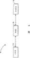
现在将参考SLDRAM存储系统对本发明的典型实施例作描述。然而,本发明同样也可以应用于其它类型的存储系统。在图1中示出了可应用本发明的典型SLDRAM系统。它包括多个被存储控制器13访问并控制的SLDRAM模块11a…11n。存储控制器13向每一个包括在反向和非反向时钟信号通道上的时钟信号CCLK、1位FLAG信号和10位指令总线CA0-9的SLDRAM模块11a…11n提供指令链接。另外,SLDRAM输入/输出信号SO和SI都以串行菊花链的形式由存储控制器13向SLDRAM模块11a…11n提供。另外,如双向数据时钟DCLKO和DCLDI一样,在存储控制器13和每个SLDRAM模块11a…11n之间提供双向数据总线DQ0-17。时钟DCLKO被用于选通进入SLDRAM模块和该模块出来的输入/输出数据,以及对之DCLDI信号通道也间歇地使用的过程。Exemplary embodiments of the present invention will now be described with reference to an SLDRAM memory system. However, the invention is equally applicable to other types of storage systems. A typical SLDRAM system to which the present invention can be applied is shown in FIG. 1 . It includes a plurality of SLDRAM modules 11 a . . . 11 n accessed and controlled by a
图2示出了SLDRAM模块11a…11n之一的简化相关部分。它包括控制逻辑电路21、锁存器23、25、49和59、可为环延迟设备的延迟设备27、29、31、55和57、缓冲器35、37、39、33、45、47、51和53、延迟锁环41、多路复用器43、流水线电路61和63、SRAM输入/输出电路65和67以及分别为存储组组0和组1的69和71。应该指出的是,虽然在图2中示出了两个存储器组,但这只是为了描述,可以使用任何数目的存储器组。Figure 2 shows a simplified relevant part of one of the SLDRAM modules 11a...11n. It comprises control logic 21, latches 23, 25, 49 and 59, delay devices 27, 29, 31, 55 and 57 which may be ring delay devices, buffers 35, 37, 39, 33, 45, 47, 51 and 53, delay locked loop 41, multiplexer 43, pipeline circuits 61 and 63, SRAM input/output circuits 65 and 67, and memory banks 69 and 71 for
控制逻辑电路21在CA0-9总线上接收并分析指令,并控制存储器组69和71的输出/输出(I/O)访问操作。控制逻辑电路21还接收FLAG信号和时钟信号CCLK。Control logic circuit 21 receives and analyzes instructions on the CA0-9 bus, and controls output/output (I/O) access operations of memory banks 69 and 71 . The control logic circuit 21 also receives the FLAG signal and the clock signal CCLK.
传送每个指令总线通道CA0-9上的信号通过各个可调节的环延迟电路27并进入各个锁存器23,在该锁存器中,信号在被缓冲器39缓冲、被延迟312延迟以及被缓冲器33缓冲的同时被CCLK信号锁存。Signals on each command bus lane CA0-9 are routed through respective adjustable loop delay circuits 27 and into respective latches 23 where they are buffered by buffer 39, delayed by delay 312 and The buffer 33 is latched by the CCLK signal while buffering.
信号CCLK还从缓冲器39通过进入到将16个时钟信号提供到多路复用器43的延迟锁环电路41。多路复用器通过各个缓冲器45向18个将从存储器组69和71输出的数据锁存的锁存器49提供18个时钟输出信号。从存储器组69和71输出的数据进入SRAM 65和67,后者起到I/O缓冲的作用并在被送入锁存器49之前通过流水线电路61。在锁存器49中锁存的输出数据被提供给各个缓冲放大器47,并从该处通过数据总线DQ被送回存储控制器13。Signal CCLK also passes from buffer 39 into delay locked loop circuit 41 which provides 16 clock signals to multiplexer 43 . The multiplexer supplies 18 clock output signals to 18 latches 49 that latch the data output from the memory banks 69 and 71 through the respective buffers 45 . Data output from memory banks 69 and 71 enters SRAMs 65 and 67, which act as I/O buffers and pass through pipeline circuit 61 before being fed into latch 49. The output data latched in the latches 49 are supplied to the respective buffer amplifiers 47, and from there are sent back to the
输入到存储器组69和71的数据由DQ数据总线上的存储控制器13供应,并通过每个数据总线通道上通过环延迟57的门控缓冲器51被送入锁存器59,通过流水线电路63。从流水线电路63,在DQ总线上的输入数据通过缓冲SRAM 65和67并进入存储器组69和71。Data input to memory banks 69 and 71 is supplied by
只要当存储控制器指示用WRITE指令在指令总线CA0-9上的数据中进行存储器访问WRITE操作时,控制逻辑电路21也会发出起动指令RXEN。RXEN指令起动数据输入缓冲器51和数据时钟输入缓冲器53。数据时钟DCLK通过门控缓冲器53、延迟电路55并被用于控制锁存器59,使它锁存在数据总线DQ上的输入数据。As long as the storage controller instructs to use the WRITE command to perform a memory access WRITE operation on the data on the command bus CA0-9, the control logic circuit 21 will also issue the activation command RXEN. The RXEN command activates the data input buffer 51 and the data clock input buffer 53 . Data clock DCLK passes through gated buffer 53, delay circuit 55 and is used to control latch 59 to latch incoming data on data bus DQ.
为了保证由SLDRAM模块11a…11n完成的多种存储器操作的准确定时,图2的电路必须是同步以保证,输入的数据相对于时钟信号CCLK和DCLK被准确定时。为了该目的,在于2000年5月10日提交的美国专利第09/568,155(律师记录:第M4065.0269)中描述的2N位同步模式被施加到每一个数据输入通道CA0-9和FLAG,同时数据模式由延迟的时钟信号CCLK在锁存器23和25采样。在该申请中描述的一种特定的16位同步模式是“1111010110010000”。In order to ensure accurate timing of the various memory operations performed by the SLDRAM modules 11a...11n, the circuit of Figure 2 must be synchronized to ensure that incoming data is accurately timed relative to the clock signals CCLK and DCLK. For this purpose, the 2N -bit synchronization pattern described in U.S. Patent No. 09/568,155 filed May 10, 2000 (Attorney's Record: No. M4065.0269) is applied to each data input channel CA0-9 and FLAG, Simultaneously the data pattern is sampled at latches 23 and 25 by the delayed clock signal CCLK. One particular 16-bit sync pattern described in that application is "1111010110010000".
取代试着判定所有的16位同步模式是否已被正确接收,本发明依靠的是在16位同步模式中从前M位序列预测下M位序列。如果接下来的序列能够被可靠地正确预测一次或多次,则同步模式被正确接收且获得了校准。如果下M位序列不能被可靠地正确预测一次或多次,则同步模式还未被正确接收,且也未获得校准,同时在校准下数据通道中的延迟值被改变,通过从前M位序列预测下M位序列可再次完成同步。该过程用跟踪那些完成数据通道校准的延迟值的控制逻辑电路重复所有可能的延迟值。控制逻辑电路21随后选择最终的延迟值,该值处于在数据通道校准中得到的那些延迟值的中心或中心附近。Instead of trying to determine whether all 16-bit sync patterns have been received correctly, the present invention relies on predicting the next M-bit sequence from the previous M-bit sequence in the 16-bit sync pattern. If the following sequence can be reliably predicted correctly one or more times, the synchronization pattern is correctly received and calibrated. If the next M-bit sequence cannot be reliably predicted correctly one or more times, the synchronization pattern has not been correctly received and has not been calibrated, while the delay value in the data channel under calibration is changed by predicting from the previous M-bit sequence The next M bit sequence can complete the synchronization again. This process is repeated for all possible delay values with the control logic tracking those delay values that complete the data channel calibration. The control logic 21 then selects a final delay value that is at or near the center of those delay values obtained in the data channel calibration.
通过保证对与不想要的时钟沿,比如反向时钟沿相关模式的下M位序列的预测,将是不正确的预测(“强行失效”)且因此将总是产生校准的缺陷,从而使本发明还保证了同步的获得是在时钟正向沿和负向沿之一想要的时钟沿上,比如在正向沿上获得的。By guaranteeing that the prediction of the lower M-bit sequence of a pattern associated with an unwanted clock edge, such as an inverted clock edge, will be an incorrect prediction ("forced invalidation") and thus will always produce a defect in alignment, this The invention also ensures that the synchronization is obtained on one of the desired clock edges, such as the positive edge, of the clock's positive and negative edges.
为了描绘校准的过程,现在将描述出现在FLAG通道上数据的校准,可以理解的是,虽然DQ总线数据通道是相对于DCLK数据选通时钟信号来完成的,但相同的校准过程也在每个指令总线CA0-9的通道和每个数据总线DQ的接收通道上进行。图3示出了时钟信号CCLK、FLAG信号、指令总线信号CA/CMD、数据总线信号DQ/DBUS以及数据选通信号DCLK的简化定时图。如图所示,在DCLK的初始PREAMBLE部分出现之后,数据总线(DBUS)的DQ通道上的4位数据(M=4)在数据时钟信号DCLK的4个顺序的正向沿和负向沿上记时。在指令信号通道CA0-9和FLAG通道上出现的数据通过指令时钟信号CCLK的四个连续的正向沿和负向沿从而以相同的方式记录时间。在图7中示出了同步模式“1111010110010000”及其与时钟信号CCLK(以及与DCLK)的关系。这些信号从存储控制器13向每一个存储模块11a…11n发送。In order to describe the calibration process, the calibration of the data appearing on the FLAG channel will now be described. It is understood that although the DQ bus data channel is done relative to the DCLK data strobe clock signal, the same calibration process is also performed on each It is performed on the channel of the command bus CA0-9 and the receiving channel of each data bus DQ. FIG. 3 shows a simplified timing diagram of the clock signal CCLK, the FLAG signal, the command bus signal CA/CMD, the data bus signal DQ/DBUS, and the data strobe signal DCLK. As shown in the figure, after the initial PREAMBLE part of DCLK, the 4-bit data (M=4) on the DQ channel of the data bus (DBUS) is on the 4 sequential positive and negative edges of the data clock signal DCLK mark time. The data appearing on the command signal channels CA0-9 and FLAG channels are timed in the same way by four consecutive positive and negative edges of the command clock signal CCLK. The synchronization pattern "1111010110010000" and its relation to the clock signal CCLK (and to DCLK) is shown in FIG. 7 . These signals are sent from the
返回到图2,可以发现,进入FLAG信号通道的数据通过环延迟电路29并被指令时钟信号CCLK锁存在锁存器25中。该数据被随后连续地施加到控制逻辑电路21。在校准期间,已知的2N位同步模式,与三个自由运行的时钟信号CCLK(图7)一起,通过存储控制器13(图1)被施加到FLAG通道。在图8中示出了用于获取校准的控制逻辑电路21的相关部分,现在将对其进行描述。Returning to FIG. 2 , it can be found that the data entering the FLAG signal channel passes through the loop delay circuit 29 and is latched in the latch 25 by the command clock signal CCLK. This data is then continuously applied to the control logic circuit 21 . During calibration, a known 2N -bit synchronous pattern is applied to the FLAG channel by memory controller 13 (FIG. 1), along with three free-running clock signals CCLK (FIG. 7). The relevant part of the control logic 21 for obtaining the calibration is shown in FIG. 8 and will now be described.
控制逻辑电路21包括4位数据捕捉寄存器101、反顺序检测器103、下一状态发生器107、启动逻辑电路105、比较器109、定时发生器111和逻辑电路113。在描述图8电路的操作以前,首先参考图7来讨论一下施加的同步模式和其对时钟信号CCLK(或DCLK)的关系。如图所示,同步模式被键为时钟信号的正向沿和负向沿(CCLK或DCLK)。在表1中示出了那些在正向沿时钟信号上初始化的四位模式以及直接跟随的下四位模式。Control logic circuit 21 includes 4-bit data capture register 101 , reverse sequence detector 103 , next state generator 107 , start logic circuit 105 , comparator 109 , timing generator 111 and logic circuit 113 . Before describing the operation of the circuit of FIG. 8, the applied synchronization pattern and its relationship to the clock signal CCLK (or DCLK) are first discussed with reference to FIG. The synchronous pattern is keyed as the positive and negative edges of the clock signal (CCLK or DCLK) as shown. In Table 1 are shown those four-bit patterns initiated on the positive-going clock signal and the next four-bit patterns immediately following.
表1Table 1
在表2中示出了在时钟负向沿初始化的四位模式以及直接跟随的下四位模式。The four-bit pattern initiated on the negative clock edge and the next four-bit pattern immediately following are shown in Table 2.
表2Table 2
本发明的一个方面就是通过将直接前M位序列预测的M位序列与接下来到达的M位序列进行比较来实现数据通道的校准。为了完成该比较,将出现在数据通道上的多个M位序列与从直接前M位序列产生的预测的M位序列进行比较。如果预测的M位序列与下M位到达的序列匹配,则已在校准下完成了数据通道的校准。如果预测的M位序列与下M位到达的序列不匹配,则校准还未完成,且控制逻辑电路21在经过校准的数据通道中改变了延迟值并再次在预测的和到达的下M位序列之间寻找匹配。为了获得更加可靠的操作,当该预测和比较过程产生了出现在数据通道上的多个M位序列的匹配时,指示该对准。也就是说,当重复的比较产生了匹配,则会发现当前的延迟值产生了校准。One aspect of the present invention is the alignment of the data path by comparing the M-bit sequence predicted by the immediately preceding M-bit sequence with the next arriving M-bit sequence. To accomplish this comparison, a plurality of M-bit sequences appearing on the data channel are compared to a predicted M-bit sequence generated from the immediately preceding M-bit sequence. If the predicted sequence of M bits matches the next arriving sequence of M bits, then the calibration of the data channel has been completed under Calibration. If the predicted M-bit sequence does not match the next M-bit arriving sequence, the calibration has not been completed and the control logic 21 changes the delay value in the calibrated data path and again compares the predicted and arriving next M-bit sequence Find a match between. For more reliable operation, the alignment is indicated when the prediction and comparison process produces a match of M-bit sequences present on the data lane. That is, when repeated comparisons yield a match, the current delay value is found to yield alignment.
在一较佳实施例中,控制逻辑电路21对校准下的数据通道实际上跨过所有可能延迟值,通知这些产生校准的延迟值并为数据通道选择最终的延迟值,该延迟值位于产生校准的延迟值的中心或中心附近。In a preferred embodiment, the control logic circuit 21 traverses virtually all possible delay values for the data channel under calibration, informs these to generate the calibration delay value and selects the final delay value for the data channel, which delay value is located at the generation calibration at or near the center of the delay value.
本发明的另一方面保证了,校准是发生在时钟信号的正向沿和负向沿的一个预定沿上,比如发生在时钟信号的正向沿上。这通过为与预定的时钟沿,比如正向沿相关的M位序列产生有效的预测值,同时为与另一时钟沿,比如负向沿相关的M位序列产生无效的预测值来完成。由于校准所不需要的时钟沿将总会具有无效预测的下一序列,所以永远都不会得到该时钟沿的校准。Another aspect of the invention ensures that the calibration occurs on a predetermined one of the positive and negative edges of the clock signal, such as on the positive edge of the clock signal. This is accomplished by generating a valid prediction value for a sequence of M bits associated with a predetermined clock edge, such as a positive going edge, while generating an invalid prediction value for a sequence of M bits associated with another clock edge, such as a negative going edge. Since a clock edge not needed for calibration will always have a next sequence of invalid predictions, it will never get calibrated for that clock edge.
返回图8,示出了经过校准的一个数据通道,比如FLAG。应该指出的是,到数据捕捉寄存器101的输入数据是从数据通道的输入锁存器,即图2中的锁存器25采集的。同时,在本发明的例子中,我们假设,到达的数据是以4位字符组(M=4)到来的,因此数据捕捉寄存器101是4级。一旦在寄存器101中存储了4位序列的同步模式,则反向序列检测器103检查存储的4位,看它们是否对应起始于系统不应该校准的时钟信号的非需要沿的位序列。在给出的例子中,我们假设,校准应该在时钟信号的正向沿上完成。因此,如果检测器103识别到匹配上述表2左列中与反向时钟沿相关的值时,它就向下一状态发生器107发送“FALL”信号。下一状态发生器107还接收存储在寄存器101中的当前位序列并从该位序列预测下4位序列应该是什么。Returning to FIG. 8 , it shows a calibrated data channel, such as FLAG. It should be noted that the input data to the data capture register 101 is captured from the input latch of the data channel, namely the latch 25 in FIG. 2 . Meanwhile, in the example of the present invention, we assume that the arriving data arrives in 4-bit bursts (M=4), so the data capture register 101 has 4 levels. Once the synchronization pattern of the 4-bit sequence is stored in the register 101, the reverse sequence detector 103 checks the stored 4 bits to see if they correspond to a bit sequence starting from an unwanted edge of the clock signal that the system should not calibrate. In the examples given, we assume that the calibration should be done on the positive edge of the clock signal. Thus, if detector 103 identifies a match with the value associated with the reverse clock edge in the left column of Table 2 above, it sends a "FALL" signal to next state generator 107 . Next state generator 107 also receives the current bit sequence stored in register 101 and predicts from this bit sequence what the next 4 bit sequence should be.
表1和表2显示了寄存器101中4位序列的16种可能性以及每一种可能性的下4位预测位序列是什么。如果下一状态发生器107未从检测器103接收到“FALL”信号,它将会产生正确的预测序列。比如,如果当前的4位序列是“1111”(表1),下一状态发生器107将产生如预测的下一位序列一样的“0101”模式。另一方面,如果下一状态发生器107从检测器103接收到了“FALL”信号,它将会产生不正确的预测序列。比如,如果当前的4位序列是“1011”(表2),则正确预测的下一位序列应该是“0010”;但是,“FALL”信号使发生器107产生了并非“0010”的其它4位模式,从而保证了不会获得数据通道的校准。Tables 1 and 2 show the 16 possibilities for the 4-bit sequence in register 101 and what the next 4-bit predicted bit sequence is for each possibility. If the next state generator 107 does not receive a "FALL" signal from the detector 103, it will generate the correct predicted sequence. For example, if the current 4-bit sequence is "1111" (Table 1), the next state generator 107 will generate a "0101" pattern as the predicted next bit sequence. On the other hand, if the next state generator 107 receives a "FALL" signal from the detector 103, it will generate an incorrect predicted sequence. For example, if the current 4-bit sequence is "1011" (Table 2), the correctly predicted next bit sequence should be "0010"; however, the "FALL" signal causes generator 107 to generate other 4-bit sequences that are not "0010". bit pattern, thus ensuring that the calibration of the data channel will not be obtained.
下一级发生器107可像图6中所示的被用作4位移位寄存器。由下一状态发生器107从启动逻辑105接收的“起始”值使它的输出成为相同重复的M位序列的2N位模式,除了一点,即它比出现在校准下数据通道上的序列提前一个M位序列。比如,启动逻辑105可启动下一状态发生器107产生初始的“0101”输出,或在初始序列之后的第一个M位序列“1111”。此后,与产生校准模式的移位寄存器操作相同的下一状态发生器107,将总是比校准模式提前M位。下一状态发生器的输出被传送到比较电路109并返回到存储控制器13(图1)。到存储控制器13的传送是控制器13的校准所需要的。The next stage generator 107 can be used as a 4-bit shift register as shown in FIG. 6 . The "start" value received by the next state generator 107 from the start logic 105 causes its output to be a 2N bit pattern of the same repeating sequence of M bits, except that it precedes the sequence appearing on the data lane under calibration A sequence of M bits. For example, enable logic 105 may enable next state generator 107 to generate an initial "0101" output, or a first sequence of M bits following an initial sequence of "1111". Thereafter, the next state generator 107, operating identically to the shift register generating the calibration pattern, will always be M bits ahead of the calibration pattern. The output of the next state generator is passed to comparison circuit 109 and back to memory controller 13 (FIG. 1). The transfer to the
比较电路109将从发生器107接收的所预测的下一位序列与寄存器101中的接着到达或现在当前的4位序列进行比较。如果比较的数据一致,则它就指示,在被校准数据通道上到达的数据用正确的时钟信号沿恰当地定时。如果数据不一致,则它就指示,还未获得这样的校准。比较的结果被施加到逻辑电路113,如果数据一致,则该逻辑电路通知环延迟(比如在所给例子中FLAG数据通道的环延迟29)的延迟值。如所指出,在较佳实施例中,逻辑电路113实际上控制环延迟,从而它用通知这些在数据通道校准中产生的延迟值的逻辑电路113来跨过所有可能的延迟值。在所有的延迟值都被跨过以后,逻辑电路113将为环延迟(比如环延迟29)设置最终的延迟值,该延迟值位于产生信号通道校准的延迟值范围的中间或中间附近。Comparison circuit 109 compares the predicted next bit sequence received from generator 107 with the next arriving or now current 4 bit sequence in register 101 . If the compared data agrees, it indicates that the data arriving on the calibrated data lane is properly timed with the correct clock edge. If the data is inconsistent, it indicates that no such calibration has been obtained. The result of the comparison is applied to a logic circuit 113 which, if the data agree, informs the delay value of the ring delay, such as the ring delay 29 of the FLAG data path in the example given. As noted, in the preferred embodiment logic 113 actually controls the loop delays so that it spans all possible delay values with logic 113 notified of these resulting delay values in data path calibration. After all delay values have been crossed, the logic circuit 113 will set a final delay value for the loop delay (such as loop delay 29 ) that is at or near the middle of the range of delay values that produced the signal path calibration.
图8还显示了启动逻辑电路105,该电路用于启动下一状态发生器107中的模式发生器,以便后者可产生在校准下数据通道上进入的相同的同步模式。检测器103和比较电路109还接收当需要数据通道校准时由控制逻辑电路21产生的起动“WRITE CALIBRATE”信号。定时发生器111接收进入的时钟信号(例子中示出的CCLK)并正确地对发生器107和比较电路109的操作进行定时。Figure 8 also shows the enable logic circuit 105 which is used to enable the pattern generator in the next state generator 107 so that the latter can generate the same synchronization pattern entered on the data channel under calibration. Detector 103 and comparison circuit 109 also receive an enable "WRITE CALIBRATE" signal generated by control logic circuit 21 when data channel calibration is required. Timing generator 111 receives an incoming clock signal (CCLK shown in the example) and correctly times the operation of generator 107 and compare circuit 109 .
虽然已结合校准时钟信号的正向沿来描述本发明的典型实施例,但它也可与时钟信号的负向沿校准,在这种情况下,表1左手栏中的模式被检测器103检测到并产生了“FALL”信号,并由此被用于在发生器107中产生无效的4位模式,同时表2左列中的4位模式被用于对接下来到达的4位模式的预测。Although the exemplary embodiment of the invention has been described in connection with calibrating the positive going edge of the clock signal, it can also be calibrated with the negative going edge of the clock signal, in which case the patterns in the left hand column of Table 1 are detected by detector 103 The "FALL" signal is received and generated and is thereby used to generate an invalid 4-bit pattern in generator 107, while the 4-bit pattern in the left column of Table 2 is used to predict the next arriving 4-bit pattern.
表2左列中的4位模式也可用于本发明的另一方面,即图1中所示的对存储控制器13的定时校准。以下的讨论假设了,与图8中所示相同的控制逻辑电路被包括在存储控制器13内。然而,这不是需要的,且其它校准存储控制器的方法通过使用存储设备和根据本发明的方法都是可行的。为了保证由SLDRAM模块11a…11n所完成的存储器操作的恰当定时,存储控制器13必须被校准,从而诸如READ或WRITE数据之类的信号,都可相对于时钟信号CCLK和DCLK被正确地定时。为了该目的,在于2000年5月10日提交的,美国专利申请第09/568,155(律师记录:第M4065.0269)中描述的一类2N位同步模式,在下一状态发生器107(图8)的存储器设备上产生且被施加到每一条返回到存储控制器13的数据通道上。如已指出,在该申请中描述的一特定的16位同步模式是“1111010110010000”。The 4-bit patterns in the left column of Table 2 can also be used in another aspect of the present invention, the timing calibration of the
返回到图8,在存储控制器的校准过程中,在下一状态发生器107产生了M位序列的2N位同步模式,且后者被传送会存储控制器13。存储控制器13可包括与图8中的所示相同的控制逻辑电路,从而调节其对应的环延迟,以便使其自身的定时与其每一个对应的指令通道CA0-9、数据通道DQ0-17以及FLAG通道的时钟信号CCLK和DCLK同步。Returning to FIG. 8 , during the calibration of the memory controller, a 2N -bit sync pattern of M-bit sequences is generated at the next state generator 107 and the latter is transmitted to the
图4示出了与在锁存器25中锁存数据的时钟信号CCLK一起的2N连续位同步模式的数据包络。数据包络的相对定时和控制数据时钟CCLK被描述成十种可能性CCLK1…10,即,环延迟29的10中可能延迟值。数据包络的开始和结束是FLAG通道上的数据不稳定的地方,它会导致错误的数据采样。如图所示,在相对定时位置C4到C7发生了可靠的数据捕捉,同时在C1…C3和C8…C10的相对定时位置上发生了不可靠的数据捕捉。这些作为延迟值D4…D7表示在控制逻辑电路21中,在该电路中,预测的4位同步模式与新到达的4位匹配。图5示出了它是怎样在控制逻辑电路21中表示的,其中在该电路中,延迟值D1…D3和D8…D10显示了表示序列匹配未被识别的“0”逻辑状态以及延迟值D4…D7的逻辑状态“1”,从而指示了预测的和接下来接收的4位序列的正确匹配。应该理解的是,虽然为了简单只显示了数据到指令时钟信号CCLK的10种相对延迟状态,但在实际操作中,对于环延迟29和图5中所示的延迟状态模式有更多可能的延迟级。FIG. 4 shows the data envelope of a 2N consecutive bit synchronous pattern together with the clock signal CCLK which latches the data in the latch 25 . The relative timing of the data envelope and the control data clock CCLK is described as ten possible CCLK1 . The start and end of the data envelope is where the data on the FLAG channel is unstable, which can lead to erroneous data sampling. As shown, reliable data capture occurs at relative timing locationsC4 throughC7 , while unreliable data capture occurs at relative timing locationsC1 ...C3 andC8 ...C10 . These are represented in the control logic circuit 21 as delay valuesD4 ...D7 where the predicted 4-bit sync pattern is matched with the newly arriving 4-bit. Figure 5 shows how this is represented in the control logic circuit 21, where the delay valuesD1 ...D3 andD8 ...D10 show a "0" logic state indicating that a sequence match is not recognized and a logic state "1" of the delay valuesD4 ...D7 , indicating a correct match of the predicted and next received 4-bit sequence. It should be understood that while only 10 relative delay states of data to instruction clock signal CCLK are shown for simplicity, in actual operation there are many more possible delays for the loop delay 29 and the delay state pattern shown in Figure 5 class.
一旦图5中所示的延迟状态模式被控制逻辑电路21推动,它便为环延迟29选择最终的延迟值,该值近似位于那些延迟值,比如D4…D7的中心,从而产生了所比较4位序列的匹配。在所示的例子中,最终的延迟将被选为D5或D6。一旦为环延迟29设置了该值,则FLAG数据通道就被校准了。Once the delay state pattern shown in FIG. 5 is driven by control logic 21, it selects final delay values for loop delay 29 that are approximately centered on those delay values, sayD4 ...D7 , resulting in the Compare matches of 4-bit sequences. In the example shown, the final delay would be chosen asD5 orD6 . Once this value is set for loop delay 29, the FLAG data path is calibrated.
对于每一个CMD数据通道CA0-9以及每一个DQ总线的数据通道,也都施加相同的校准工序,后者只有一点不同,即数据时钟DCLK被用于在出现在每个DQ数据总线的数据通道中的锁存器59中锁存数据,从而DQ数据总线的数据通道相对于DCLK时钟信号对准。For each CMD data channel CA0-9 and each data channel of the DQ bus, the same calibration process is also applied, the latter has only one difference, that is, the data clock DCLK is used to appear on the data channel of each DQ data bus The data is latched in the latch 59 in the DQ data bus so that the data lanes of the DQ data bus are aligned with respect to the DCLK clock signal.
在图6中示出了一种产生并预测了2N位模式,其中,N=4,以产生重复的16位模式。它包括了具有位位置<0><1><2><3>的四级移位寄存器151、具有分别连接于移位寄存器151<0><1><2>输出的三个输入的NOR(或非)门电路153、具有分别连接于移位寄存器151输出<3>和NOR门电路153输出的两个输入的异或门电路155,以及具有一对分别连接于异或门155输出和移位寄存器151第一级输出<0>的输入的异或门157。异或门157的输出作为移位寄存器151的级<0>输入施加。向移位寄存器151施加时钟信号CLK。移位寄存器151可用在级<0><1><2><3>上的零“0”被初始地启动且将会产生重复的16位模式“1111010110010000”。替代用电路产生重复位模式,模式也被存储在存储控制器13(图1)和下一状态发生器107(图8)中并在校准期间被重复地读取。In Fig. 6 a pattern of 2N bits is generated and predicted, where N = 4, to generate a repeating 16-bit pattern. It includes a four-
虽然本发明已结合用于预测下4位序列的M位序列进行了描述,其中M=4,但这只是本发明可被实现的一个例子。本发明可与任何少于2N位的重复同步模式一起使用,使用偶数位序列为较佳。Although the invention has been described in connection with an M-bit sequence for predicting the next 4-bit sequence, where M=4, this is only one example of how the invention can be implemented. The present invention can be used with any repeating sync pattern of less than 2N bits, preferably with even bit sequences.
如上所述的一个数据通道的校准也可用施加于邻近数据管脚和/或数据通道的同相或异相的串话元件来完成。以该方法,可在更接近地重复实际使用条件的条件下获得校准。从而,比如,当特定的数据通道,比如,FLAG如图8所示地被校准,则可向邻近的数据管脚和/或通道,比如CA0-9总线的一条同相和/或异相的邻近通道,施加相同的模式。Calibration of a data lane as described above can also be accomplished with in-phase or out-of-phase crosstalk elements applied to adjacent data pins and/or data lanes. In this way, calibration can be obtained under conditions that more closely replicate actual use conditions. Thus, for example, when a particular data channel, for example, FLAG is calibrated as shown in FIG. 8, an adjacent data pin and/or channel, such as an in-phase and/or out-of-phase adjacent channel, apply the same pattern.
还可以使用上述的技术,通过剩余的不在使用同相和/或异相校准信号校准下的数据通道来同时校准几个数据通道。比如,一半的数据通道可被表示为“受害者”且使用上述参考图4-8的技术进行同时校准,同时剩余的一半数据通道可表示为噪声源。校准将同时发生在“受害者”数据通道上,同时噪声源数据通道接收交替的同相和异相的校准信号。在“受害者”的校准之后,“受害者”和“噪声源”管脚和/或数据通道将随后被反向,且校准现在如上所述地在使用其它作为噪声源的数据通道的新“受害者”上执行。It is also possible to simultaneously calibrate several data channels with the remaining data channels not being calibrated using in-phase and/or out-of-phase calibration signals using the techniques described above. For example, half of the data channels may be represented as "victims" and simultaneously calibrated using the techniques described above with reference to Figures 4-8, while the remaining half of the data channels may be represented as noise sources. Calibration will occur simultaneously on the "victim" data channel while the noise source data channel receives alternating in-phase and out-of-phase calibration signals. After the calibration of the "victim", the "victim" and "noise source" pins and/or data lanes will then be inverted, and the calibration is now using the new " Victim" is executed.
包含校准结构和如上所述操作的存储设备可用于图9所示类型的基于处理器的系统。基于处理器的系统90包含处理器94、存储电路96以及I/O(输入/输出)设备92。存储电路96可以是SLDRAM存储电路或任何包含如根据本发明所述进行操作的校准结构的其它存储电路。另外,处理器94可本身为集成处理器,该处理器在包含本发明校准结构的芯片存储设备上使用。此外,存储控制器13(图1)可与处理器94分开,或可与其它根据以上本发明描述的存储电路96的元件一起与处理器94结合,或者处理器94本身可以起到存储控制器13的作用。A memory device containing a calibration structure and operating as described above may be used in a processor-based system of the type shown in FIG. 9 . Processor-based
在前述的讨论中,已描述的本发明的设备和方法是相关于每个时钟周期定时数据两次(即,读取或写入数据)的存储设备:既在时钟上升沿又在时钟下降沿。但是,本发明可用于任何完成校准的存储设备中,包括每个时钟周期定时数据一次的设备,比如在上升沿或下降沿之一进行。In the foregoing discussion, the devices and methods of the present invention have been described in relation to memory devices that clock data (i.e., read or write data) twice per clock cycle: both on the rising clock edge and on the falling clock edge . However, the present invention can be used in any memory device that performs calibration, including devices that clock data once every clock cycle, such as on one of the rising or falling edges.
虽然已结合了典型实施例描述和描绘了本发明,但在不脱离本发明精神和范围的条件下可有多种变化和代替的等效形式。因此,本发明并不能被理解成由上述描述作出的限制,本发明只被所附权利要求的范围限制。While the invention has been described and illustrated in conjunction with typical embodiments, there may be various changes and substitution of equivalents without departing from the spirit and scope of the invention. Accordingly, the invention is not to be seen as limited by the foregoing description, but the invention is only limited by the scope of the appended claims.
Claims (117)
Applications Claiming Priority (2)
| Application Number | Priority Date | Filing Date | Title |
|---|---|---|---|
| US09/568,016 | 2000-05-10 | ||
| US09/568,016US6606041B1 (en) | 2000-05-10 | 2000-05-10 | Predictive timing calibration for memory devices |
Related Child Applications (1)
| Application Number | Title | Priority Date | Filing Date |
|---|---|---|---|
| CNA2008101314227ADivisionCN101320593A (en) | 2000-05-10 | 2001-05-07 | Predictive timing calibration for memory devices |
Publications (2)
| Publication Number | Publication Date |
|---|---|
| CN1636248A CN1636248A (en) | 2005-07-06 |
| CN100407181Ctrue CN100407181C (en) | 2008-07-30 |
Family
ID=24269573
Family Applications (2)
| Application Number | Title | Priority Date | Filing Date |
|---|---|---|---|
| CN018112277AExpired - Fee RelatedCN100407181C (en) | 2000-05-10 | 2001-05-07 | Predictive timing calibration for storage devices |
| CNA2008101314227APendingCN101320593A (en) | 2000-05-10 | 2001-05-07 | Predictive timing calibration for memory devices |
Family Applications After (1)
| Application Number | Title | Priority Date | Filing Date |
|---|---|---|---|
| CNA2008101314227APendingCN101320593A (en) | 2000-05-10 | 2001-05-07 | Predictive timing calibration for memory devices |
Country Status (10)
| Country | Link |
|---|---|
| US (2) | US6606041B1 (en) |
| EP (3) | EP1282677B1 (en) |
| JP (1) | JP4649629B2 (en) |
| KR (1) | KR100580740B1 (en) |
| CN (2) | CN100407181C (en) |
| AT (3) | ATE384327T1 (en) |
| AU (1) | AU2001259571A1 (en) |
| DE (3) | DE60139355D1 (en) |
| TW (1) | TW588375B (en) |
| WO (1) | WO2001085884A2 (en) |
Families Citing this family (37)
| Publication number | Priority date | Publication date | Assignee | Title |
|---|---|---|---|---|
| US7137048B2 (en)* | 2001-02-02 | 2006-11-14 | Rambus Inc. | Method and apparatus for evaluating and optimizing a signaling system |
| US6735709B1 (en)* | 2000-11-09 | 2004-05-11 | Micron Technology, Inc. | Method of timing calibration using slower data rate pattern |
| US6873939B1 (en) | 2001-02-02 | 2005-03-29 | Rambus Inc. | Method and apparatus for evaluating and calibrating a signaling system |
| US7490275B2 (en) | 2001-02-02 | 2009-02-10 | Rambus Inc. | Method and apparatus for evaluating and optimizing a signaling system |
| US7058799B2 (en)* | 2001-06-19 | 2006-06-06 | Micron Technology, Inc. | Apparatus and method for clock domain crossing with integrated decode |
| US7668276B2 (en) | 2001-10-22 | 2010-02-23 | Rambus Inc. | Phase adjustment apparatus and method for a memory device signaling system |
| EP1865648B1 (en) | 2001-10-22 | 2012-12-05 | Rambus Inc. | Phase adjustment apparatus and method for a memory device signalling system |
| US7469328B1 (en)* | 2003-02-06 | 2008-12-23 | Cisco Technology, Inc. | Synchronization technique for high speed memory subsystem |
| US7076377B2 (en)* | 2003-02-11 | 2006-07-11 | Rambus Inc. | Circuit, apparatus and method for capturing a representation of a waveform from a clock-data recovery (CDR) unit |
| US7336749B2 (en)* | 2004-05-18 | 2008-02-26 | Rambus Inc. | Statistical margin test methods and circuits |
| US7590175B2 (en)* | 2003-05-20 | 2009-09-15 | Rambus Inc. | DFE margin test methods and circuits that decouple sample and feedback timing |
| US7627029B2 (en) | 2003-05-20 | 2009-12-01 | Rambus Inc. | Margin test methods and circuits |
| US7646835B1 (en)* | 2003-11-17 | 2010-01-12 | Rozas Guillermo J | Method and system for automatically calibrating intra-cycle timing relationships for sampling signals for an integrated circuit device |
| US8422568B2 (en) | 2004-01-28 | 2013-04-16 | Rambus Inc. | Communication channel calibration for drift conditions |
| US7400670B2 (en) | 2004-01-28 | 2008-07-15 | Rambus, Inc. | Periodic calibration for communication channels by drift tracking |
| US7095789B2 (en)* | 2004-01-28 | 2006-08-22 | Rambus, Inc. | Communication channel calibration for drift conditions |
| US6961862B2 (en) | 2004-03-17 | 2005-11-01 | Rambus, Inc. | Drift tracking feedback for communication channels |
| US7079446B2 (en) | 2004-05-21 | 2006-07-18 | Integrated Device Technology, Inc. | DRAM interface circuits having enhanced skew, slew rate and impedance control |
| US8099638B2 (en)* | 2004-11-12 | 2012-01-17 | Ati Technologies Ulc | Apparatus and methods for tuning a memory interface |
| US7509515B2 (en)* | 2005-09-19 | 2009-03-24 | Ati Technologies, Inc. | Method and system for communicated client phase information during an idle period of a data bus |
| US7362107B2 (en)* | 2005-11-08 | 2008-04-22 | Mediatek Inc. | Systems and methods for automatically eliminating imbalance between signals |
| US7571267B1 (en) | 2006-03-27 | 2009-08-04 | Integrated Device Technology, Inc. | Core clock alignment circuits that utilize clock phase learning operations to achieve accurate clocking of data derived from serial data streams having different relative skews |
| US7706996B2 (en)* | 2006-04-21 | 2010-04-27 | Altera Corporation | Write-side calibration for data interface |
| US8504865B2 (en)* | 2007-04-20 | 2013-08-06 | Easic Corporation | Dynamic phase alignment |
| TWI421694B (en)* | 2009-08-26 | 2014-01-01 | Asustek Comp Inc | Memory controlling method |
| US8943242B1 (en) | 2012-03-30 | 2015-01-27 | Integrated Device Technology Inc. | Timing controllers having partitioned pipelined delay chains therein |
| US9846606B2 (en)* | 2014-11-07 | 2017-12-19 | Mediatek Inc. | Storage device calibration methods and controlling device using the same |
| US9607672B2 (en) | 2014-11-14 | 2017-03-28 | Cavium, Inc. | Managing skew in data signals with adjustable strobe |
| US9570128B2 (en)* | 2014-11-14 | 2017-02-14 | Cavium, Inc. | Managing skew in data signals |
| US9502099B2 (en) | 2014-11-14 | 2016-11-22 | Cavium, Inc. | Managing skew in data signals with multiple modes |
| CN108241586B (en)* | 2016-12-27 | 2020-03-06 | 慧荣科技股份有限公司 | Controller circuit and estimated delay compensation method |
| KR102378384B1 (en)* | 2017-09-11 | 2022-03-24 | 삼성전자주식회사 | Operation method of nonvolatile memory device and operation method of memory controller |
| CN109656846B (en)* | 2018-12-20 | 2020-11-17 | 湖南国科微电子股份有限公司 | Method and device for optimizing available delay parameter interval of electronic terminal and memory |
| US11210029B2 (en)* | 2020-05-18 | 2021-12-28 | Micron Technology, Inc. | Generating memory array control signals |
| US11361815B1 (en) | 2020-12-24 | 2022-06-14 | Winbond Electronics Corp. | Method and memory device including plurality of memory banks and having shared delay circuit |
| KR20240029250A (en) | 2022-08-26 | 2024-03-05 | 에스케이하이닉스 주식회사 | Semiconductor device and semiconductor system |
| CN117478107B (en)* | 2023-12-28 | 2024-02-27 | 芯光智网集成电路设计(无锡)有限公司 | Delay calibration method, transmitting end and source synchronous communication system |
Citations (3)
| Publication number | Priority date | Publication date | Assignee | Title |
|---|---|---|---|---|
| CN1061485A (en)* | 1990-11-14 | 1992-05-27 | 国际商业机器公司 | The system and method for restore data in the multiple head assembly storage |
| WO1999046687A1 (en)* | 1998-03-12 | 1999-09-16 | Hitachi, Ltd. | Data transmitter |
| US6041419A (en)* | 1998-05-27 | 2000-03-21 | S3 Incorporated | Programmable delay timing calibrator for high speed data interface |
Family Cites Families (9)
| Publication number | Priority date | Publication date | Assignee | Title |
|---|---|---|---|---|
| US4755951A (en)* | 1986-03-03 | 1988-07-05 | Tektronix, Inc. | Method and apparatus for digitizing a waveform |
| US4791404A (en)* | 1986-03-03 | 1988-12-13 | Tektronix, Inc. | Predictive time base control circuit for a waveform system |
| IL96808A (en) | 1990-04-18 | 1996-03-31 | Rambus Inc | Integrated circuit i/o using a high performance bus interface |
| US5266952A (en)* | 1992-03-30 | 1993-11-30 | Hughes Aircraft Company | Feed forward predictive analog-to-digital converter |
| US5917760A (en) | 1996-09-20 | 1999-06-29 | Sldram, Inc. | De-skewing data signals in a memory system |
| US5953263A (en) | 1997-02-10 | 1999-09-14 | Rambus Inc. | Synchronous memory device having a programmable register and method of controlling same |
| US6016282A (en) | 1998-05-28 | 2000-01-18 | Micron Technology, Inc. | Clock vernier adjustment |
| US6349399B1 (en)* | 1998-09-03 | 2002-02-19 | Micron Technology, Inc. | Method and apparatus for generating expect data from a captured bit pattern, and memory device using same |
| US6430696B1 (en)* | 1998-11-30 | 2002-08-06 | Micron Technology, Inc. | Method and apparatus for high speed data capture utilizing bit-to-bit timing correction, and memory device using same |
- 2000
- 2000-05-10USUS09/568,016patent/US6606041B1/ennot_activeExpired - Lifetime
- 2001
- 2001-05-07CNCN018112277Apatent/CN100407181C/ennot_activeExpired - Fee Related
- 2001-05-07ATAT01933122Tpatent/ATE384327T1/ennot_activeIP Right Cessation
- 2001-05-07KRKR1020027015063Apatent/KR100580740B1/ennot_activeExpired - Fee Related
- 2001-05-07CNCNA2008101314227Apatent/CN101320593A/enactivePending
- 2001-05-07EPEP01933122Apatent/EP1282677B1/ennot_activeExpired - Lifetime
- 2001-05-07JPJP2001582474Apatent/JP4649629B2/ennot_activeExpired - Fee Related
- 2001-05-07ATAT09005437Tpatent/ATE492881T1/ennot_activeIP Right Cessation
- 2001-05-07AUAU2001259571Apatent/AU2001259571A1/ennot_activeAbandoned
- 2001-05-07EPEP09005437Apatent/EP2077558B1/ennot_activeExpired - Lifetime
- 2001-05-07DEDE60139355Tpatent/DE60139355D1/ennot_activeExpired - Lifetime
- 2001-05-07WOPCT/US2001/014658patent/WO2001085884A2/enactiveIP Right Grant
- 2001-05-07DEDE60132445Tpatent/DE60132445T2/ennot_activeExpired - Lifetime
- 2001-05-07ATAT07023120Tpatent/ATE437438T1/ennot_activeIP Right Cessation
- 2001-05-07DEDE60143726Tpatent/DE60143726D1/ennot_activeExpired - Lifetime
- 2001-05-07EPEP07023120Apatent/EP1927988B1/ennot_activeExpired - Lifetime
- 2001-07-23TWTW090111186Apatent/TW588375B/ennot_activeIP Right Cessation
- 2003
- 2003-02-13USUS10/365,399patent/US6674378B2/ennot_activeExpired - Lifetime
Patent Citations (3)
| Publication number | Priority date | Publication date | Assignee | Title |
|---|---|---|---|---|
| CN1061485A (en)* | 1990-11-14 | 1992-05-27 | 国际商业机器公司 | The system and method for restore data in the multiple head assembly storage |
| WO1999046687A1 (en)* | 1998-03-12 | 1999-09-16 | Hitachi, Ltd. | Data transmitter |
| US6041419A (en)* | 1998-05-27 | 2000-03-21 | S3 Incorporated | Programmable delay timing calibrator for high speed data interface |
Also Published As
| Publication number | Publication date |
|---|---|
| US20030122696A1 (en) | 2003-07-03 |
| WO2001085884A2 (en) | 2001-11-15 |
| DE60132445T2 (en) | 2008-08-14 |
| EP2077558A1 (en) | 2009-07-08 |
| ATE437438T1 (en) | 2009-08-15 |
| DE60143726D1 (en) | 2011-02-03 |
| JP2003532969A (en) | 2003-11-05 |
| DE60139355D1 (en) | 2009-09-03 |
| KR20030013407A (en) | 2003-02-14 |
| US6674378B2 (en) | 2004-01-06 |
| TW588375B (en) | 2004-05-21 |
| AU2001259571A1 (en) | 2001-11-20 |
| ATE384327T1 (en) | 2008-02-15 |
| CN101320593A (en) | 2008-12-10 |
| KR100580740B1 (en) | 2006-05-15 |
| JP4649629B2 (en) | 2011-03-16 |
| DE60132445D1 (en) | 2008-03-06 |
| EP1927988B1 (en) | 2009-07-22 |
| US6606041B1 (en) | 2003-08-12 |
| ATE492881T1 (en) | 2011-01-15 |
| EP1282677B1 (en) | 2008-01-16 |
| EP2077558B1 (en) | 2010-12-22 |
| CN1636248A (en) | 2005-07-06 |
| EP1282677A2 (en) | 2003-02-12 |
| WO2001085884A3 (en) | 2002-05-23 |
| EP1927988A1 (en) | 2008-06-04 |
Similar Documents
| Publication | Publication Date | Title |
|---|---|---|
| CN100407181C (en) | Predictive timing calibration for storage devices | |
| US6434081B1 (en) | Calibration technique for memory devices | |
| US6338127B1 (en) | Method and apparatus for resynchronizing a plurality of clock signals used to latch respective digital signals, and memory device using same | |
| US6889357B1 (en) | Timing calibration pattern for SLDRAM | |
| US5822255A (en) | Semiconductor integrated circuit for supplying a control signal to a plurality of object circuits | |
| US6279090B1 (en) | Method and apparatus for resynchronizing a plurality of clock signals used in latching respective digital signals applied to a packetized memory device | |
| US6707723B2 (en) | Data input circuits and methods of inputting data for a synchronous semiconductor memory device | |
| US6414903B1 (en) | Method and apparatus for crossing clock domain boundaries | |
| US6259288B1 (en) | Semiconductor integrated circuit having a DLL circuit and a special power supply circuit for the DLL circuit | |
| US20040187046A1 (en) | Method of timing calibration using slower data rate pattern | |
| US6807500B2 (en) | Method and apparatus providing improved data path calibration for memory devices | |
| US7379383B2 (en) | Methods of DDR receiver read re-synchronization | |
| US7634698B2 (en) | Semiconductor integrated circuit with full-speed data transition scheme for DDR SDRAM at internally doubled clock testing application | |
| GB2320779A (en) | Synchronous semiconductor memory device | |
| US7587645B2 (en) | Input circuit of semiconductor memory device and test system having the same | |
| JP2006505866A (en) | Data acquisition method and apparatus | |
| KR20210034219A (en) | Signal generation circuit and semiconductor apparatus using the signal generation circuit | |
| US20020036533A1 (en) | Timing controller and controlled delay circuit for controlling timing or delay time of a signal by changing phase thereof | |
| US7016256B2 (en) | Data input unit of synchronous semiconductor memory device, and data input method using the same | |
| JPH11185492A (en) | Self clock logic circuit and method for latching its output signal | |
| CN111868831A (en) | Apparatus and method for tuning a phase mixer circuit | |
| US7493461B1 (en) | Dynamic phase alignment for resynchronization of captured data | |
| KR100320775B1 (en) | Signal Control Circuits, Clock Control Circuits and Semiconductor Memory | |
| CN119626284A (en) | Information transmission method, memory, control device and electronic device |
Legal Events
| Date | Code | Title | Description |
|---|---|---|---|
| C06 | Publication | ||
| PB01 | Publication | ||
| C10 | Entry into substantive examination | ||
| SE01 | Entry into force of request for substantive examination | ||
| C14 | Grant of patent or utility model | ||
| GR01 | Patent grant | ||
| C17 | Cessation of patent right | ||
| CF01 | Termination of patent right due to non-payment of annual fee | Granted publication date:20080730 Termination date:20110507 |