CN100405610C - Wiring layered structure formed in contact hole, manufacturing method of wiring layered structure, and display device having the wiring layered structure - Google Patents
Wiring layered structure formed in contact hole, manufacturing method of wiring layered structure, and display device having the wiring layered structureDownload PDFInfo
- Publication number
- CN100405610C CN100405610CCNB031043801ACN03104380ACN100405610CCN 100405610 CCN100405610 CCN 100405610CCN B031043801 ACNB031043801 ACN B031043801ACN 03104380 ACN03104380 ACN 03104380ACN 100405610 CCN100405610 CCN 100405610C
- Authority
- CN
- China
- Prior art keywords
- layer
- insulating layer
- wiring
- metal
- layered structure
- Prior art date
- Legal status (The legal status is an assumption and is not a legal conclusion. Google has not performed a legal analysis and makes no representation as to the accuracy of the status listed.)
- Expired - Fee Related
Links
Images


Classifications
- H—ELECTRICITY
- H05—ELECTRIC TECHNIQUES NOT OTHERWISE PROVIDED FOR
- H05B—ELECTRIC HEATING; ELECTRIC LIGHT SOURCES NOT OTHERWISE PROVIDED FOR; CIRCUIT ARRANGEMENTS FOR ELECTRIC LIGHT SOURCES, IN GENERAL
- H05B33/00—Electroluminescent light sources
- H—ELECTRICITY
- H10—SEMICONDUCTOR DEVICES; ELECTRIC SOLID-STATE DEVICES NOT OTHERWISE PROVIDED FOR
- H10D—INORGANIC ELECTRIC SEMICONDUCTOR DEVICES
- H10D30/00—Field-effect transistors [FET]
- H10D30/01—Manufacture or treatment
- H10D30/021—Manufacture or treatment of FETs having insulated gates [IGFET]
- H10D30/031—Manufacture or treatment of FETs having insulated gates [IGFET] of thin-film transistors [TFT]
- H10D30/0312—Manufacture or treatment of FETs having insulated gates [IGFET] of thin-film transistors [TFT] characterised by the gate electrodes
- H10D30/0314—Manufacture or treatment of FETs having insulated gates [IGFET] of thin-film transistors [TFT] characterised by the gate electrodes of lateral top-gate TFTs comprising only a single gate
- H—ELECTRICITY
- H10—SEMICONDUCTOR DEVICES; ELECTRIC SOLID-STATE DEVICES NOT OTHERWISE PROVIDED FOR
- H10D—INORGANIC ELECTRIC SEMICONDUCTOR DEVICES
- H10D30/00—Field-effect transistors [FET]
- H10D30/01—Manufacture or treatment
- H10D30/021—Manufacture or treatment of FETs having insulated gates [IGFET]
- H10D30/031—Manufacture or treatment of FETs having insulated gates [IGFET] of thin-film transistors [TFT]
- H10D30/0321—Manufacture or treatment of FETs having insulated gates [IGFET] of thin-film transistors [TFT] comprising silicon, e.g. amorphous silicon or polysilicon
- H—ELECTRICITY
- H10—SEMICONDUCTOR DEVICES; ELECTRIC SOLID-STATE DEVICES NOT OTHERWISE PROVIDED FOR
- H10D—INORGANIC ELECTRIC SEMICONDUCTOR DEVICES
- H10D30/00—Field-effect transistors [FET]
- H10D30/60—Insulated-gate field-effect transistors [IGFET]
- H10D30/67—Thin-film transistors [TFT]
- H10D30/6729—Thin-film transistors [TFT] characterised by the electrodes
- H10D30/6737—Thin-film transistors [TFT] characterised by the electrodes characterised by the electrode materials
- H—ELECTRICITY
- H10—SEMICONDUCTOR DEVICES; ELECTRIC SOLID-STATE DEVICES NOT OTHERWISE PROVIDED FOR
- H10D—INORGANIC ELECTRIC SEMICONDUCTOR DEVICES
- H10D30/00—Field-effect transistors [FET]
- H10D30/60—Insulated-gate field-effect transistors [IGFET]
- H10D30/67—Thin-film transistors [TFT]
- H10D30/674—Thin-film transistors [TFT] characterised by the active materials
- H10D30/6741—Group IV materials, e.g. germanium or silicon carbide
- H10D30/6743—Silicon
- H—ELECTRICITY
- H10—SEMICONDUCTOR DEVICES; ELECTRIC SOLID-STATE DEVICES NOT OTHERWISE PROVIDED FOR
- H10K—ORGANIC ELECTRIC SOLID-STATE DEVICES
- H10K59/00—Integrated devices, or assemblies of multiple devices, comprising at least one organic light-emitting element covered by group H10K50/00
- H10K59/10—OLED displays
- H10K59/12—Active-matrix OLED [AMOLED] displays
- Y—GENERAL TAGGING OF NEW TECHNOLOGICAL DEVELOPMENTS; GENERAL TAGGING OF CROSS-SECTIONAL TECHNOLOGIES SPANNING OVER SEVERAL SECTIONS OF THE IPC; TECHNICAL SUBJECTS COVERED BY FORMER USPC CROSS-REFERENCE ART COLLECTIONS [XRACs] AND DIGESTS
- Y10—TECHNICAL SUBJECTS COVERED BY FORMER USPC
- Y10T—TECHNICAL SUBJECTS COVERED BY FORMER US CLASSIFICATION
- Y10T428/00—Stock material or miscellaneous articles
- Y10T428/12—All metal or with adjacent metals
- Y10T428/12493—Composite; i.e., plural, adjacent, spatially distinct metal components [e.g., layers, joint, etc.]
- Y10T428/12528—Semiconductor component
- Y—GENERAL TAGGING OF NEW TECHNOLOGICAL DEVELOPMENTS; GENERAL TAGGING OF CROSS-SECTIONAL TECHNOLOGIES SPANNING OVER SEVERAL SECTIONS OF THE IPC; TECHNICAL SUBJECTS COVERED BY FORMER USPC CROSS-REFERENCE ART COLLECTIONS [XRACs] AND DIGESTS
- Y10—TECHNICAL SUBJECTS COVERED BY FORMER USPC
- Y10T—TECHNICAL SUBJECTS COVERED BY FORMER US CLASSIFICATION
- Y10T428/00—Stock material or miscellaneous articles
- Y10T428/24—Structurally defined web or sheet [e.g., overall dimension, etc.]
- Y10T428/24802—Discontinuous or differential coating, impregnation or bond [e.g., artwork, printing, retouched photograph, etc.]
- Y10T428/24917—Discontinuous or differential coating, impregnation or bond [e.g., artwork, printing, retouched photograph, etc.] including metal layer
Landscapes
- Internal Circuitry In Semiconductor Integrated Circuit Devices (AREA)
- Electroluminescent Light Sources (AREA)
- Thin Film Transistor (AREA)
- Electrodes Of Semiconductors (AREA)
Abstract
Translated fromChinese
Description
Translated fromChinese技术领域technical field
本发明涉及配线分层结构,配线分层结构的制作方法,以及包括该配线分层结构的显示装置。The invention relates to a wiring layered structure, a manufacturing method of the wiring layered structure, and a display device including the wiring layered structure.
背景技术Background technique
最近市场上已出现采用薄膜晶体管(下文将间称为TFT)作为开关元件的显示装置。作为替代CRT和LCD的显示装置,采用起发光元件作用的电流驱动型有机发光二极管(下文称之为OLED)的有机电致发光(EL)显示装置的当前已呈现出巨大的吸引力。在采用有机电致发光(EL)元件的显示装置中,TFT也用于驱动有机EL元件。Display devices using thin film transistors (hereinafter referred to as TFTs) as switching elements have appeared in the market recently. As a display device replacing CRT and LCD, an organic electroluminescent (EL) display device employing a current-driven organic light emitting diode (hereinafter referred to as OLED) functioning as a light emitting element has currently shown great attraction. In display devices employing organic electroluminescent (EL) elements, TFTs are also used to drive the organic EL elements.
图5是使用有机EL元件的显示装置中的TFT的剖面图。TFT 200具有一个层叠的结构,该结构是这样的顺序,即由石英玻璃等等制成的绝缘基片,由多晶硅制成的有源层243,由SiO2(二氧化硅)制成的栅极绝缘薄膜212,以及由诸如钼(Mo)之类耐熔性金属制成的栅极电极242。向有源层243提供了在栅极电极242下面的沟道243c以及漏极243d和源极243s,漏极243d和源极243s是在沟道243c的两端以栅极电极242作为掩膜采用离子注入的方法制成的。5 is a cross-sectional view of a TFT in a display device using an organic EL element. The TFT 200 has a laminated structure in this order of an insulating substrate made of quartz glass or the like, an
TFT 200还包括层间薄膜215,漏极电极253和源极电极254,所述层间薄膜包括由SiN制成的第一层间绝缘薄膜213和由SiO2制成的第二层间绝缘薄膜214。漏极电极253和源极电极254是通过在分别对应于漏极243d和源极243s而提供的接触孔中填入铝或类似金属形成的。在形成漏极电极253和源极电极254中所使用的接触孔是采用氢氟酸缓冲液蚀刻而成的。The TFT 200 also includes an interlayer film 215 including a first interlayer
然而,在如上构成的TFT中,当使用氢氟酸缓冲液时,由SiN制成的第一层间绝缘薄膜213具有比构成第二层间绝缘薄膜214的SiO2低的腐蚀速率。于是,如果采用氢氟酸缓冲液的湿蚀刻法来形成接触孔,会在栅极绝缘薄膜212和第一层间绝缘薄膜213之间边界上形成伸臂,如图6A所示,在该伸臂处栅极绝缘薄膜212被腐蚀较多。这类伸臂的形成可引起增加的接触电阻的问题,这是由于在各自的接触孔中所形成的漏极电极253和源极电极254之间的水平差产生的。However, in the TFT constituted as above, when a hydrofluoric acid buffer solution is used, the first
另一方面,利用采用有机EL元件的显示装置,要求包含用作有机EL元件电源线的配线的驱动TFT具有较高的可靠性,这要通过诸如降低电阻、减少毛刺和小丘或消除电迁移或应力迁移之类的手段来实现。为了获得较低的电阻,由诸如上述铝之类的低电阻金属构成漏极电极253和源极电极254。而且,通过提供由诸如钼之类的耐熔性金属制成的保护金属层,以覆盖由诸如铝之类的低电阻金属制成的配线层的方式,来减少毛刺和小丘。这样形成的保护金属层比由低电阻金属制成的配线层更薄,以便于从整体上减小配线的电阻以及减少平面表面的非均匀性。On the other hand, with a display device using an organic EL element, high reliability is required for a drive TFT including a wiring used as a power supply line of the organic EL element, which is achieved by means such as lowering resistance, reducing burrs and hillocks, or eliminating electric current. Migration or stress migration and other means to achieve. In order to obtain lower resistance, the drain electrode 253 and the source electrode 254 are formed of a low-resistance metal such as the aforementioned aluminum. Also, burrs and hillocks are reduced by providing a protective metal layer made of a refractory metal such as molybdenum to cover a wiring layer made of a low-resistance metal such as aluminum. The protective metal layer thus formed is thinner than the wiring layer made of low-resistance metal, so as to reduce the resistance of the wiring as a whole and reduce unevenness of the planar surface.
当漏极电极253和源极电极254是由低电阻金属的配线层和保护金属层构成时,会引起保护金属层断裂的问题,这是由于在接触孔中形成的伸臂引起的水平差而造成的,如图6B所示。而且,正如上述所说明的那样,在断裂的部分会产生毛刺。特别是,因为有机EL元件的阴极形成在漏极电极253和元件电极254的整个表面上,所以生长在保护金属层上的毛刺就会引起在这些电极和有机EL元件的阴极之间的短路,从而致使显示装置的缺陷。When the drain electrode 253 and the source electrode 254 are composed of a wiring layer of a low-resistance metal and a protective metal layer, there is a problem that the protective metal layer is broken due to the level difference caused by the overhang formed in the contact hole. resulting, as shown in Figure 6B. Furthermore, as explained above, burrs are generated at the broken parts. Particularly, since the cathode of the organic EL element is formed on the entire surface of the drain electrode 253 and the element electrode 254, a burr growing on the protective metal layer will cause a short circuit between these electrodes and the cathode of the organic EL element, Thus causing a defect of the display device.
发明内容Contents of the invention
鉴于上述情况,作出本发明,其一个目的是提供一种能通过防止电极之间的短路而减少有缺陷的显示装置的出现的配线分层结构。本发明的另一目的是减少在配线分层结构中毛刺的发生。本发明还有一个目的是降低配线分层结构的电阻。The present invention has been made in view of the above circumstances, and an object thereof is to provide a wiring layered structure capable of reducing the occurrence of defective display devices by preventing short circuits between electrodes. Another object of the present invention is to reduce the occurrence of burrs in the wiring layered structure. Yet another object of the present invention is to reduce the electrical resistance of the wiring layer structure.
根据本发明,提供了一种配线分层结构,该配线分层结构提供于绝缘薄膜中形成的接触孔中,在所述绝缘薄膜中,彼此由不同材料制成的第一绝缘层和第二绝缘层依次层叠,并且该配线分层结构包括:由耐熔性金属制成的第一金属层;由电阻比耐熔性金属的电阻低的金属制成的形成于第一金属层上的配线层;以及由耐熔性金属制成的且厚度比第一绝缘层厚的形成于配线层上的第二金属层。According to the present invention, there is provided a wiring layered structure provided in a contact hole formed in an insulating film in which the first insulating layer and the first insulating layer made of different materials are mutually different. The second insulating layer is laminated in sequence, and the wiring layered structure includes: a first metal layer made of a refractory metal; and a second metal layer formed on the wiring layer, which is made of a refractory metal and thicker than the first insulating layer.
通过形成比第一绝缘层厚的第二金属层,即使当在接触孔处的第一和第二绝缘层之间边界上形成伸臂时,也可能形成第二金属层而不发生任何断裂。结果,可以防止在第二金属层上形成毛刺,使得不会在该配线分层结构和其它电极之间引起短路。By forming the second metal layer thicker than the first insulating layer, even when an overhang is formed on the boundary between the first and second insulating layers at the contact hole, it is possible to form the second metal layer without any breakage. As a result, burrs can be prevented from being formed on the second metal layer, so that no short circuit is caused between the wiring layered structure and other electrodes.
第一绝缘层可以由SiO2或SiON制成。而且,第二绝缘层可以由SiN制成。The first insulating layer can be made ofSiO2 or SiON. Also, the second insulating layer may be made of SiN.
作为耐熔性金属,可使用包括6A族元素的金属,例如,钼(Mo),铬(Cr)或钨(W)。这样的一层金属层的提供有利于减少在互连结构中的毛刺和小丘的发生。而且,这些6A族的元素具有比低电阻金属低的扩散特性。此外,钛(Ta),钒(V)或铌(Nb)也可以作为耐熔性金属使用。值得推荐的是耐熔性金属包括钼。特别是,钼在制造过程中易于处理。As the refractory metal, a metal including a group 6A element such as molybdenum (Mo), chromium (Cr) or tungsten (W) can be used. The provision of such a metal layer is beneficial to reduce the occurrence of burrs and hillocks in the interconnect structure. Also, these Group 6A elements have lower diffusion characteristics than low-resistance metals. In addition, titanium (Ta), vanadium (V) or niobium (Nb) can also be used as the refractory metal. It is recommended that refractory metals include molybdenum. Molybdenum, in particular, is easy to handle during manufacturing.
作为构成配线层的金属来说,可以使用例如铝(Al),铜(Cu),银(Ag),金(Au),铑(Rh),铱(Ir),镍(Ni),铂(Pt)或钯(Pd)。通过使用上述这些金属,可以制成具有低电阻的配线分层结构。在这些金属中,推荐使用特别是铝,以及电阻率比铝低的铜或银。特别推荐配线分层结构是由含有铝的金属制成。从而,加强了铝与耐熔性金属制成的金属层的粘结,因为铝的反应性高,从而有利于提高配线分层结构的产量。As the metal constituting the wiring layer, for example, aluminum (Al), copper (Cu), silver (Ag), gold (Au), rhodium (Rh), iridium (Ir), nickel (Ni), platinum ( Pt) or palladium (Pd). By using these metals as described above, a wiring layered structure with low resistance can be made. Among these metals, aluminum in particular, and copper or silver having a lower resistivity than aluminum are recommended. It is particularly recommended that the wiring layer structure is made of a metal containing aluminum. Thereby, the adhesion of aluminum to the metal layer made of refractory metal is enhanced, since the reactivity of aluminum is high, thereby contributing to the improvement of the yield of the wiring layered structure.
根据本发明,提供了一种配线分层结构,该配线分层结构提供于绝缘薄膜中形成的接触孔中,在绝缘薄膜中,彼此由不同材料制成的第一绝缘层和第二绝缘层依次层叠,且该配线分层结构包括:由耐熔性金属所制成的第一金属层;由电阻比耐熔性金属低的金属制成的形成于第一金属层上的配线层;由耐熔性金属制成的且厚度比伸臂与伸臂下的第1绝缘层之间的距离厚的形成于所述配线层上的第二金属层,其中通过使用预定腐蚀剂形成所述接触孔,且在所述第二绝缘薄膜中形成了所述伸臂,该伸臂朝向接触孔中心而凸出于第1绝缘薄膜之外。According to the present invention, there is provided a wiring layered structure provided in a contact hole formed in an insulating film in which a first insulating layer and a second insulating layer made of different materials are mutually different. Insulating layers are stacked in sequence, and the wiring layered structure includes: a first metal layer made of a refractory metal; a wiring layer; a second metal layer formed on said wiring layer made of refractory metal and thicker than the distance between the outrigger and the first insulating layer under the outrigger, wherein by using a predetermined etchant The contact hole is formed, and the extension arm is formed in the second insulating film, and the extension arm protrudes out of the first insulating film toward the center of the contact hole.
通过形成厚度比在接触孔处的第二绝缘薄膜上形成的伸臂与伸臂下的第一绝缘薄膜之间的距离厚的第二金属层,由于伸臂的效应可以被吸收,所以就有可能在不会出现任何断裂的情况下形成第二金属层。于是,可以防止在第二金属层上毛刺的形成,使得不会引起在该配线分层结构和其它电极之间的短路。要理解的是,在这种情况下,能够形成厚度比在伸臂的尖端和伸臂下的第一绝缘薄膜之间的距离厚的第二金属层。By forming the second metal layer thicker than the distance between the arm formed on the second insulating film at the contact hole and the first insulating film under the arm, since the effect of the arm can be absorbed, there is It is possible to form the second metal layer without any breakage. Thus, the formation of burrs on the second metal layer can be prevented so as not to cause short circuits between the wiring layered structure and other electrodes. It is understood that in this case, the second metal layer can be formed thicker than the distance between the tip of the arm and the first insulating film under the arm.
氢氟酸缓冲液可以作为预定的腐蚀剂使用。Buffered hydrofluoric acid can be used as the intended etchant.
根据本发明,提供了一种配线分层结构,该配线分层结构提供于绝缘薄膜中形成的接触孔中,在绝缘薄膜中,彼此由不同材料制成的第一绝缘层和第二绝缘层依次层叠,且该配线分层结构包括:由耐熔性金属所制成的第一金属层;由电阻比耐熔性金属低的金属制成的形成于第一金属层上的配线层;由耐熔性金属制成的形成于配线层上的第二金属层,且形成的第二金属层具有一定的厚度使得在使用预定的腐蚀剂时,由于第一绝缘层和第二绝缘层的不同腐蚀速率而引起的水平差而造成的任何断裂都不会发生,其中所述接触孔是通过采用预定的腐蚀剂形成的。According to the present invention, there is provided a wiring layered structure provided in a contact hole formed in an insulating film in which a first insulating layer and a second insulating layer made of different materials are mutually different. Insulating layers are stacked in sequence, and the wiring layered structure includes: a first metal layer made of a refractory metal; A wire layer; a second metal layer formed on the wiring layer made of a refractory metal, and the second metal layer is formed to have a certain thickness so that when a predetermined etchant is used, due to the first insulating layer and the second Any cracking due to level difference due to different etching rates of the insulating layer, wherein the contact hole is formed by using a predetermined etchant, does not occur.
通过因此形成第二金属层,就可能在不发生任何断裂的情况下形成第二金属层。于是,就能防止在第二金属层上形成毛刺,使得不会在该配线分层结构和其它电极之间引起短路。By thus forming the second metal layer, it is possible to form the second metal layer without any breakage. Thus, it is possible to prevent burrs from being formed on the second metal layer, so that no short circuit is caused between the wiring layered structure and other electrodes.
可采用这样的方法形成接触孔,即第二绝缘层具有比第一绝缘层更平坦的锥度。The contact hole may be formed in such a way that the second insulating layer has a flatter taper than the first insulating layer.
通过将第二绝缘层的锥度制成得比第一绝缘层的锥度更为平坦,能够减少伸臂的效应,使得第二金属层的厚度可以制得更薄。于是,就能使该配线分层结构是低电阻的。By making the taper of the second insulating layer flatter than that of the first insulating layer, the effect of the outrigger can be reduced, so that the thickness of the second metal layer can be made thinner. Thus, the wiring layered structure can be made to be low-resistance.
绝缘薄膜可以进一步包括第三层绝缘层,它形成于第二绝缘层上,且当使用预定的腐蚀剂时,该第三绝缘层由具有腐蚀速率大于第二绝缘层材料的腐蚀速率的材料制成。在第二绝缘层是SiN的情况下,第三绝缘层可以由SiO2或SiON制成。通过提供诸如上述的第三绝缘层之类的另一绝缘层,在腐蚀过程中,该第三绝缘层的腐蚀快于第二绝缘层,使得第二绝缘层从上面被腐蚀且第二绝缘层的锥度可以变得更平坦。The insulating film may further include a third insulating layer formed on the second insulating layer, and when a predetermined etchant is used, the third insulating layer is made of a material having an etching rate greater than that of the material of the second insulating layer . In case the second insulating layer is SiN, the third insulating layer may be made ofSiO2 or SiON. By providing another insulating layer, such as the third insulating layer described above, which etches faster than the second insulating layer during etching, so that the second insulating layer is etched from above and the second insulating layer The taper can become flatter.
可形成第二绝缘层,使得第二绝缘层的厚的大于或等于第一绝缘层的厚度,且小于或等于大约600nm。The second insulating layer may be formed such that the thickness of the second insulating layer is greater than or equal to that of the first insulating layer and less than or equal to about 600 nm.
通过以这样的方法,即第二绝缘层的厚度大于或等于第一绝缘层的厚度,来形成第二绝缘层,可使第二绝缘层的锥度比第一绝缘层的锥度更加平坦。而且,通过以这样的方式,即第二绝缘层的厚度小于或等于600nm,来形成第二绝缘层,就能控制形成接触孔所需要的蚀刻时间,使得可以适当地限制接触孔的扩展。By forming the second insulating layer in such a way that the thickness of the second insulating layer is greater than or equal to the thickness of the first insulating layer, the taper of the second insulating layer can be made flatter than that of the first insulating layer. Also, by forming the second insulating layer in such a manner that the thickness of the second insulating layer is less than or equal to 600 nm, the etching time required to form the contact hole can be controlled so that the expansion of the contact hole can be appropriately limited.
可把第一金属层形成为比第一绝缘层厚。通过形成比第一绝缘层厚的第一金属层,即使在接触孔处的第一和第二绝缘层之间的边界上形成了伸臂时,也可能在没有任何断裂发生的情况下形成第一金属层。结果,可以防止在第一金属层上毛刺的形成,使得不会在该配线分层结构和其它电极之间引起短路。The first metal layer may be formed thicker than the first insulating layer. By forming the first metal layer thicker than the first insulating layer, even when an outrigger is formed on the boundary between the first and second insulating layers at the contact hole, it is possible to form the first metal layer without any crack occurring. a metal layer. As a result, the formation of burrs on the first metal layer can be prevented so that no short circuit is caused between the wiring layered structure and other electrodes.
上述的配线分层结构可用于半导体器件,该半导体器件包括在基片和第一绝缘层之间提供的半导体层,和在不同于第一绝缘层上形成的接触孔的位置上提供的栅极电极。在这种情况下,第一绝缘层起栅极绝缘薄膜的作用,而第二绝缘层起栅极绝缘薄膜或层间绝缘薄膜的作用。可以这样的方式,即第一和第二绝缘层由接触孔贯通,来形成所述接触孔,以便于配线与半导体层相连接。The wiring layered structure described above can be used in a semiconductor device including a semiconductor layer provided between a substrate and a first insulating layer, and a gate electrode provided at a position different from a contact hole formed on the first insulating layer. pole electrode. In this case, the first insulating layer functions as a gate insulating film, and the second insulating layer functions as a gate insulating film or an interlayer insulating film. The contact hole may be formed in such a manner that the first and second insulating layers are penetrated by the contact hole, so that the wiring is connected to the semiconductor layer.
根据本发明,提供了一种制造配线分层结构的方法,该方法包括:通过用预定的腐蚀剂蚀刻,在绝缘薄膜上形成接触孔,在所述绝缘薄膜中彼此由不同材料制成的第一绝缘层和第二绝缘层依次层叠;在接触孔中形成由耐熔性金属制成的第一金属层;在第一金属层上形成配线层,该配线层是由电阻低于耐熔性金属的电阻的金属所制成;以及在配线层上形成由耐熔性金属制成的第二金属层,使得其厚度厚于第一绝缘层。According to the present invention, there is provided a method of manufacturing a wiring layered structure, the method comprising: forming a contact hole in an insulating film in which first electrodes made of different materials from each other are formed by etching with a predetermined etchant. An insulating layer and a second insulating layer are stacked in sequence; a first metal layer made of refractory metal is formed in the contact hole; a wiring layer is formed on the first metal layer, and the wiring layer is made of a resistance lower than the resistance and a second metal layer made of a refractory metal is formed on the wiring layer so as to be thicker than the first insulating layer.
接触孔的形成可以是这样的,即通过使用一种腐蚀剂来进行蚀刻,所述腐蚀剂对第一绝缘层的腐蚀速率比对第二绝缘层的腐蚀速率高。The contact hole may be formed by performing etching by using an etchant having a higher etching rate for the first insulating layer than for the second insulating layer.
根据本发明,提供了一种显示装置,该显示装置包括上述配线分层结构中的任一种,以及至少具有在所述配线分层结构上提供的阳极,发光元件层和阴极的光学元件中。According to the present invention, there is provided a display device comprising any one of the above wiring layered structures, and an optical optical device having at least an anode provided on the wiring layered structure, a light emitting element layer and a cathode. element.
根据本发明,提供了一种显示装置,它包括:在形成于绝缘薄膜之中的接触孔中提供的配线分层结构,在所述绝缘薄膜中彼此由不同材料制成的第一绝缘层和第二绝缘层依次层叠;以及光学元件,它形成在所述配线分层结构上,且至少具有阳极、发光元件和阴极,其中所述配线分层结构包括:由耐熔性金属制成的第一金属层;形成于第一金属层上的配线层,它由电阻低于耐熔性金属的电阻的金属制成;以及第二金属层,它形成于配线层上且其厚度比第一绝缘层厚。According to the present invention, there is provided a display device comprising: a wiring layered structure provided in a contact hole formed in an insulating film in which first insulating layers made of different materials from each other and a second insulating layer; and an optical element formed on the wiring layered structure and having at least an anode, a light emitting element, and a cathode, wherein the wiring layered structure includes: made of a refractory metal a first metal layer formed on the first metal layer; a wiring layer formed on the first metal layer, which is made of a metal whose resistance is lower than that of the refractory metal; and a second metal layer, which is formed on the wiring layer and whose The thickness is thicker than the first insulating layer.
通过形成厚度比第一绝缘层厚的第二金属层,即使在接触孔处的第一和第二绝缘层的边界形成了伸臂时,也可能在没有任何断裂发生的情况下形成第二金属层。结果,能够防止在第二金属层上形成毛刺,使得在该配线分层结构和上述提供的光学元件的电极之间不会引起短路。特别是当所形成的光学元件的阴极共同用于显示装置的多个像素时,对配线分层结构和阴极之间的短路的防止可以显著地降低显示装置出现缺陷的几率。By forming the second metal layer thicker than the first insulating layer, it is possible to form the second metal without any fracture even when an overhang is formed at the boundary of the first and second insulating layers at the contact hole. layer. As a result, burrs can be prevented from being formed on the second metal layer, so that no short circuit is caused between the wiring layered structure and the electrodes of the optical element provided above. Especially when the cathode of the formed optical element is commonly used for a plurality of pixels of the display device, the prevention of short circuit between the wiring layer structure and the cathode can significantly reduce the probability of defects in the display device.
要注意,作为当前实施例以及当前实施例所包含的内容,上述所讨论的结构组件的任一组合,以及在方法和装置之间表述的变化都是有效的。It is to be noted that any combination of the above-discussed structural components, as well as changes expressed between methods and apparatuses, are valid as the present embodiment and the contents contained in the present embodiment.
然而,本发明的概述没有必要描述所有必要特征,以致于本发明也是上述特征的一个子组合。However, the summary of the invention does not necessarily describe all necessary features, so that the invention is also a sub-combination of the above-mentioned features.
附图说明Description of drawings
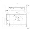
图1是显示装置部分的平面示意图。Fig. 1 is a schematic plan view of a portion of a display device.
图2是图1所示的显示像素中的由虚线所指示和包围的区域的剖面图。FIG. 2 is a cross-sectional view of a region indicated and surrounded by a dotted line in the display pixel shown in FIG. 1 .
图3A至3D说明了形成接触孔、源极电极和漏极电极的过程。3A to 3D illustrate the process of forming a contact hole, a source electrode and a drain electrode.
图4是解释本发明第二实施例的示意图。Fig. 4 is a schematic diagram for explaining a second embodiment of the present invention.
图5是采用有机EL元件的显示装置中的常规TFT的剖面图。Fig. 5 is a cross-sectional view of a conventional TFT in a display device using an organic EL element.
图6A和6B是有机EL元件的常规TFT中的接触孔的剖面图。6A and 6B are sectional views of a contact hole in a conventional TFT of an organic EL element.
具体实施方式Detailed ways
将基于较佳实施例来描述本发明,这些较佳实施例并不限制本发明的范围而是用于解释本发明。在实施例中所描述的所有特征及其组合对于本发明不是必要的。The present invention will be described based on preferred embodiments which do not limit the scope of the present invention but serve to explain the present invention. All features and combinations thereof described in the exemplary embodiments are not essential to the invention.
第一实施例first embodiment
根据本发明第一实施例的配线分层结构用于驱动包括有机EL元件的显示装置的TFT。图1是显示该显示装置的部分的平面图。显示装置100包括由图1中的短划线所指示的于绝缘的基片10上的显示区域110,以及用于驱动显示区域的TFT的外围驱动电路120和130。多条扫描线G1至Gm与外围驱动电路120相连接,以及多条数据线D1至Dn与外围驱动电路130相连接。The wiring layered structure according to the first embodiment of the present invention is used to drive TFTs of a display device including organic EL elements. FIG. 1 is a plan view showing part of the display device. The
参照图1,在显示区域110中所显示的是一个电路图,它用于接近扫描线Gk和数据线Dk相交点的显示像素。该显示像素包括有机EL元件60,第一TFT 30,第二TFT 40和电容器C。Referring to FIG. 1, displayed in a
在第一TFT 30中的栅极电极与扫描线Gk相连接,第一TFT 30中的源极电极(或漏极电极)与数据线Dk相连接,第一TFT 30中的漏极电极(或源极电极)与第二TFT40的栅极电极和电容器C的电极之一相连接。The gate electrode in the
第二TFT 40的栅极电极与TFT 30的漏极电极(或源极电极)相连接。TFT 40的源极电极与有机EL元件的阳极相连接,TFT 40的漏极电极与电源线112相连接。有机EL元件60实际发光所需的电压提供到电源线112上。电容器C的电极之一与TFT 30的漏极电极(或源极电极)以及与TFT 40的栅极电极相连接。电容器C的另一电极接地。有机EL元件60的阳极与第二TFT 40的源极电极相连接,以及有机EL元件60的阴极接地。The gate electrode of the
图2是图1中所示的虚线包围的区域150的剖面图。参照图2,在玻璃、石英或类似材料制成的绝缘基片10上形成有源层43。有源层43是由通过激光对非晶硅(a-Si)薄膜照射而进行多晶化后的多晶硅(p-Si)薄膜制成的。在有源层43中,沟道43c的两边提供了源极43s和漏极43d。FIG. 2 is a cross-sectional view of the
在有源层43上形成了栅极绝缘薄膜12,又在栅极绝缘薄膜12上形成了栅极电极42。栅极电极42是由诸如铬和钼之类的耐熔性金属制成。该栅极电极42与第一TFT 30的源极相连接。在有源层43中,在栅极电极42下形成沟道43c。The
在栅极绝缘薄膜12和栅极电极42的整个表面上形成层间绝缘薄膜15。相对于漏极43d和源极43s而形成的接触孔由诸如铝之类的金属填充,以形成漏极电极53和源极电极54。后面将描述接触孔,漏极电极53和源极电极54的形成方法。The
在层间绝缘薄膜15,漏极电极53和源极电极54的整个表面上形成平面化的绝缘薄膜17,它是由例如有机树脂制成的。在平面化的绝缘薄膜17上形成有机EL元件60。有机EL元件具有阳极61,发光元件层66以及阴极67依次沉积的结构。阳极61通过相对于平面化的绝缘薄膜17中的源极电极54而形成的接触孔与源极43s相连接。在阳极61上形成绝缘薄膜68。所形成的绝缘薄膜68用于防止在阴极67和阳极61之间的短路,这种短路是由于阳极61的厚度所产生的阶差或水平差异使发光元件层66断裂而引起的。On the entire surfaces of the
适用于阳极61的材料的例子包括:氧化锡铟(ITO)、二氧化锡(SnO2)以及氧化铟(In2O3)。一般来说,常使用ITO,因为其具有空穴注入的有效性和低的表面电阻。阴极67材料的例子包括:含有微量锂的铝合金、镁铟合金、以及镁银合金。发光元件层66具有空穴传输层62、发光层64以及电子传输层65依次沉积的结构。适用于空穴传输层62材料的例子包括:4,4’,4”-三氨基甲烷盐酸缓冲液(tris)(3-甲基苯基苯基氨基)三苯氨(triphenylamine)(MTDATA),N,N’-Di(萘(naphthalene)-1-y1)-N,N’-联苯(diphenyl)-对二氨基联苯(benzidine)(NPB)以及N,N’-联苯(diphenyl)-N,N’-di(3-甲基苯基)-1,1’-联苯(biphenyl)-4,4’-二胺(diamine)(TPD)。发光层64的材料的例子包括:双(bis)(苯并喹啉并)(benzoquinolinolato)铍合成物,含有一种喹吖(二)酮(quinacridone)衍生物(双(10-羟基苯[h]喹啉并)镀(bis(10-hydroxybenzo[h]quinolinolato)beryllium):Bebq2)和铝-喹啉(quinolene)合成物(Alq3)。电子传输层65的材料例子包括:Bebq2和Alq3。Examples of materials suitable for the anode 61 include: indium tin oxide (ITO), tin dioxide (SnO2 ), and indium oxide (In2 O3 ). In general, ITO is often used because of its effectiveness in hole injection and low surface resistance. Examples of materials for the
形成了空穴传输层62,电子传输层65和阴极67,使得它们由每个像素中的多个有机EL元件60共享。响应于阳极61把光发射层64形成为岛。The
上述对于一个像素的结构和材料仅仅是说明性的,而不是对本发明的范围的限制。例如,第一TFT 30和第二TFT 40可以是n沟道类型、p沟道类型或甚至是n沟道类型和p沟道类型的组合。有机EL元件60可以具有以相反次序沉积的阳极61、发光元件层66和阴极67的结构。在这些层之间可以形成介入层。The structure and material of a pixel mentioned above are only illustrative, rather than limiting the scope of the present invention. For example, the
现在将描述在如此配置的像素中的有机EL元件60发光操作。当将来自扫描线Gk的栅极信号施加到第一TFT 30的栅极电极时,第一TFT 30就被开启。于是,从第一TFT 30的源极(或漏极)电极施加的电荷就存储在电容器C上,同时也施加到第二TFT 40的栅极电极。响应于施加到第二TFT 40的栅极电极的电压的电流从驱动电源线112馈送至有机EL元件60。The light emitting operation of the
在有机EL元件60中,为了产生激发,从阳极61注入的空穴和从阴极67注入的电子在光发射层64的内部重新结合,使构成光发射层64的有机分子激发。在能量发射激发的失活过程中,光发射层64发出光,它通过传输阳极61放电并被认为是有机EL元件60的光发射。In the
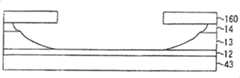
将根据上述所说明的有机EL显示器的像素结构来描述本发明的特征。在本发明的一个实施例中,漏极电极53和源极电极54都具有多层结构,该多层结构包括低电阻金属制成的配线层和耐熔性金属制成的保护金属层,其中将配线层设置在保护金属层之间。至于第一实施例,形成的保护金属层要比栅极绝缘薄膜12厚。Features of the present invention will be described based on the pixel structure of the organic EL display explained above. In one embodiment of the present invention, both the
图3A至3D显示了形成接触孔,漏极电极53和源极电极54的方法的一系列过程。在本发明的第一实施例中,栅极薄膜12是由使用CVD方法形成的二氧化硅(SiO2)制成的。层间绝缘薄膜15包括由使用CVD方法形成的氮化硅(SiN)制成的第一层间绝缘薄膜13和同样由使用CVD方法形成的二氧化硅(SiO2)制成的第二层间绝缘薄膜14。这些第一层间绝缘薄膜13和第二层间绝缘薄膜14最好能采用CVD方法连续形成而不需要移出真空条件。如此,可以防止空气中的灰尘和杂质粘结在这两层薄膜之间的界面上。3A to 3D show a series of processes of the method of forming the contact hole, the
下文继续描述形成接触孔的方法。采用氢氟酸缓冲液并利用在对应于有源层43(见图2)的源极43s(或漏极43d)的位置上有开孔的抗蚀层160作为掩膜进行蚀刻。如图3A所示,首先通过蚀刻除去第二层间绝缘薄膜14。这时,处于抗蚀层160之下的第二层间绝缘薄膜14也受到蚀刻。The method of forming a contact hole is continued below. Etching is performed using a hydrofluoric acid buffer solution and using the resist
接着,如图3B所示,通过蚀刻除去了第一层间绝缘薄膜13。此时,当使用氢氟酸缓冲液时,在第一层间绝缘薄膜13被腐蚀的同时,腐蚀速率大于第一层间绝缘薄膜13的腐蚀速率的第二层间绝缘薄膜14以侧向方向被进一步蚀刻。结果,第一层间绝缘薄膜13从上面被蚀刻掉,而第一层间绝缘薄膜13的锥形角度也能变得更小些。Next, as shown in FIG. 3B, the first
如图3C所示,当第一层间绝缘薄膜13的蚀刻完成之后,开始了对栅极绝缘薄膜12的蚀刻。不仅在垂直方向,而且在水平方向对栅极绝缘薄膜12进行蚀刻。此时,第一层间绝缘薄膜13也被蚀刻,但是当使用氢氟酸缓冲液时,栅极绝缘薄膜12的腐蚀速率大于第一层间绝缘薄膜13的腐蚀速率,所以比起第一层间绝缘薄膜13,栅极绝缘薄膜12进一步以水平方向受到蚀刻。结果,如该图所示,在第一层间绝缘薄膜13和栅极绝缘薄膜12之间的边界可能形成伸臂。这里所讨论的伸臂是在第一层间绝缘薄膜13上形成的,它向着第一层间绝缘薄膜13和栅极绝缘薄膜12之间边界上的接触孔的中心而凸出于栅极绝缘薄膜12之外。如此,将贯穿栅极绝缘薄膜12、第一层间绝缘薄膜13和第二层间绝缘薄膜14的接触孔形成于对应于有源层43的漏极14d(或源极14s)的位置上。As shown in FIG. 3C, after the etching of the first
除去抗蚀层160,随后如图3D所示,采用溅射技术在接触孔和第二层间绝缘薄膜14的整个表面上连续形成由耐熔性金属制成的第一保护金属层170、由低电阻金属制成的配线层172以及由耐熔性金属制成的第二保护金属层174。此时,所形成的第二保护金属层174比栅极绝缘薄膜12厚。然后,蚀刻第一保护金属层170、配线层172和第二保护金属层174,以形成漏极电极53和源极电极54。The resist
在该第一实施例中,通过形成比栅极绝缘薄膜12厚的第二保护金属层174,即使当第一层间绝缘薄膜13和栅极绝缘薄膜12之间的边界上形成了伸臂时,也可能在没有任何断裂发生的情况下形成第二保护金属层174。结果,能够抑制掉在漏极电极53和源极电极54上毛刺的发生。因此,如图2所示,即使当有机EL元件60的阴极67形成于漏极电极53和源极电极54的整个表面上,也不会引起任何短路,从而实现了显示装置100(图1中所示)的稳定生产。In this first embodiment, by forming the second
而且,在本实施例中,形成的第一保护金属层170也厚于栅极绝缘薄膜12。这可以抑制在漏极电极53和源极电极54上发生毛刺。因此,不会在漏极电极53和源极电极54和其它电极之间引起任何短路,从而实现显示装置100的稳定生产。Moreover, in this embodiment, the first
另外,在本实施例中,形成的第一层间绝缘薄膜13具有比栅极绝缘薄膜12厚的厚度。结果,用于从上蚀刻第一层间绝缘薄膜13所需的时间就变得更长,从而就有可能使得第一层间绝缘薄膜13的锥度角度变得更加平缓。而且,由于当使用氢氟酸缓冲液时,由腐蚀速率高于第一层间绝缘薄膜13的材料制成的第二层间绝缘薄膜14形成于第一层间绝缘薄膜之上,因此用于从上蚀刻第一层间绝缘薄膜13所需的时间就会变得更长,从而有可能使第一层间绝缘薄膜13具有更加平缓的锥度角度。In addition, in the present embodiment, the first
而且,可以这样的方式,即接触孔最宽部分的半径小于所希望的值,来形成第一层间绝缘薄膜13。例如,根据本实施例,所形成的接触孔最宽部分的半径可以为(2+α)μm(式中α是抗蚀层160的开孔的半径,且按照本实施例,α约为2μm)或小于(2+α)μm。参照图3C,如果栅极绝缘薄膜12(SiO2)的厚度、第一层间绝缘薄膜13(SiN)的厚度以及第二层间绝缘薄膜14(SiO2)的厚度分别以d1、d2和d3来表示,且当使用氢氟酸缓冲液时它们的腐蚀速率分别以r1、r2和r3表示,则总的蚀刻时间T将为T=d1/r1+d2/r2+d3/r3。Also, the first
接触孔进入到第二层间绝缘薄膜14的扩展L将为L=r3×T。因此,栅极绝缘薄膜12、第一层间绝缘薄膜13和第二层间绝缘薄膜14将形成为某一厚度,使得L=r3×T≤2μm(公式1)。在本实施例中,栅极绝缘薄膜12和第二层间绝缘薄膜14都是由SiO2制成的,因此有可能使
在满足所有上述条件的情况下,第一层间绝缘薄膜13的较佳的厚度范围为100至600nm。第二层间绝缘薄膜14的较佳的厚度范围为100至500nm。栅极氧化薄膜12的较佳厚度范围为20至100nm。第一保护金属层170的较佳的厚度范围为30至120nm。第二保护金属层174的较佳的厚度范围为30至120nm以及配线层172的较佳厚度范围为30至700nm。Under the condition that all the above conditions are satisfied, the preferred thickness range of the first
第二实施例second embodiment
图4是解释本发明第二实施例的示意图。Fig. 4 is a schematic diagram for explaining a second embodiment of the present invention.
在第一实施例中,描述是针对形成的第二保护金属层174的厚度厚于栅极绝缘薄膜12的情况。然而,在该第二实施例中,形成第二保护金属层174,是第二保护金属层174的薄膜厚度d5大于伸臂的尖端和伸臂之下的栅极绝缘薄膜12之间的距离d4。从而,即使当第一层间绝缘薄膜13和栅极绝缘薄膜12之间的边界上形成了伸臂时,也将在不发生任何断裂的情况下形成第二保护金属层174。结果,能够抑制从漏极电极53和源极电极54生长的毛刺的发生。因此,如图2所示,当有机EL元件60的阴极67形成于漏极电极53和源极电极54的整个表面上时,不会引起任何短路,从而实现了显示装置100的稳定生产。In the first embodiment, the description is directed to the case where the second
而且,在该第二实施例中,所形成的第一保护金属层170的厚度d6也大于伸臂的尖端和伸臂之下的栅极绝缘薄膜12之间的距离d4。从而,能够获得类似的效果,其中能够防止电极之间的短路。Moreover, in the second embodiment, the thickness d6 of the formed first
在上述描述的实施例中,栅极绝缘薄膜12和第二层间绝缘薄膜14都是采用SiO2制成的,但栅极绝缘薄膜12和第二层间绝缘薄膜14也可以采用SiON(氮氧化硅)制成。当采用预定蚀刻剂进行蚀刻来形成贯穿多层结构中的薄膜的孔,且构成多层结构的低层的材料的腐蚀速率大于构成多层结构的上层的材料的腐蚀速率时,可以有效地使用根据本发明的配线分层结构以及该配线分层结构的制造方法。In the embodiment described above, the
而且,在上述实施例中,第一层间绝缘薄膜13是由SiN制成的,但例如SiN所制成的层也可以用于在栅极绝缘薄膜12上的第二栅极绝缘薄膜。Also, in the above-described embodiment, the first
虽然已通过示例性实施例描述了本发明,但是应该理解到,在不脱离所附的权利要求所规定的本发明范围的条件下,本领域的技术人员可以作出许多变化和替代。Although the invention has been described by way of exemplary embodiments, it should be understood that many changes and substitutions can be made by those skilled in the art without departing from the scope of the invention as defined in the appended claims.
Claims (18)
Translated fromChineseApplications Claiming Priority (2)
| Application Number | Priority Date | Filing Date | Title |
|---|---|---|---|
| JP2002059151 | 2002-03-05 | ||
| JP2002059151AJP2003258094A (en) | 2002-03-05 | 2002-03-05 | Wiring structure, method of manufacturing the same, and display device |
Publications (2)
| Publication Number | Publication Date |
|---|---|
| CN1442838A CN1442838A (en) | 2003-09-17 |
| CN100405610Ctrue CN100405610C (en) | 2008-07-23 |
Family
ID=27784733
Family Applications (1)
| Application Number | Title | Priority Date | Filing Date |
|---|---|---|---|
| CNB031043801AExpired - Fee RelatedCN100405610C (en) | 2002-03-05 | 2003-02-10 | Wiring layered structure formed in contact hole, manufacturing method of wiring layered structure, and display device having the wiring layered structure |
Country Status (4)
| Country | Link |
|---|---|
| US (2) | US6717218B2 (en) |
| JP (1) | JP2003258094A (en) |
| KR (1) | KR100504051B1 (en) |
| CN (1) | CN100405610C (en) |
Families Citing this family (9)
| Publication number | Priority date | Publication date | Assignee | Title |
|---|---|---|---|---|
| US7579251B2 (en)* | 2003-05-15 | 2009-08-25 | Fujitsu Limited | Aerosol deposition process |
| KR101052960B1 (en)* | 2004-04-29 | 2011-07-29 | 엘지디스플레이 주식회사 | Semi-transmissive polysilicon liquid crystal display device manufacturing method |
| KR20060020017A (en)* | 2004-08-30 | 2006-03-06 | 삼성에스디아이 주식회사 | Electron emitting device and method for manufacturing same |
| TWI253872B (en)* | 2004-09-23 | 2006-04-21 | Au Optronics Corp | Organic electro-luminescence device and method for forming the same |
| KR100700650B1 (en)* | 2005-01-05 | 2007-03-27 | 삼성에스디아이 주식회사 | Organic electroluminescent device and manufacturing method thereof |
| WO2008013402A1 (en)* | 2006-07-25 | 2008-01-31 | Lg Chem, Ltd. | Method of manufacturing organic light emitting device and organic light emitting device manufactured by using the method |
| CN101919043B (en)* | 2008-01-21 | 2013-06-05 | 金振有限公司 | Display device |
| KR101135540B1 (en) | 2009-11-30 | 2012-04-13 | 삼성모바일디스플레이주식회사 | Organic Light Emitting Display Device |
| CN104051542B (en)* | 2014-06-23 | 2016-10-05 | 上海和辉光电有限公司 | Organic light emitting display device and thin film transistor thereof |
Citations (3)
| Publication number | Priority date | Publication date | Assignee | Title |
|---|---|---|---|---|
| JPH0582656A (en)* | 1991-03-19 | 1993-04-02 | Matsushita Electric Ind Co Ltd | Semiconductor device and its manufacture |
| JPH08204009A (en)* | 1995-01-30 | 1996-08-09 | Ricoh Co Ltd | Semiconductor device and method of manufacturing the semiconductor device |
| CN1184335A (en)* | 1996-11-28 | 1998-06-10 | 现代电子产业株式会社 | Semiconductor device and method for forming metal interconnection in semiconductor device |
Family Cites Families (44)
| Publication number | Priority date | Publication date | Assignee | Title |
|---|---|---|---|---|
| US3662210A (en)* | 1970-04-28 | 1972-05-09 | Viktor Fedorovich Maximov | Electrode for pulse high-power electrovacuum devices |
| JPH0673023B2 (en) | 1984-12-10 | 1994-09-14 | 三井石油化学工業株式会社 | Thermal fixing type electrophotographic developer |
| JPH084153B2 (en) | 1987-04-08 | 1996-01-17 | 沖電気工業株式会社 | Light emitting diode drive circuit |
| JP2946921B2 (en) | 1992-03-10 | 1999-09-13 | 日本電気株式会社 | Low power drive circuit |
| US5517080A (en)* | 1992-12-14 | 1996-05-14 | Westinghouse Norden Systems Inc. | Sunlight viewable thin film electroluminescent display having a graded layer of light absorbing dark material |
| EP0738014B1 (en)* | 1993-08-05 | 2003-10-15 | Matsushita Electric Industrial Co., Ltd. | Manufacturing method of semiconductor device having high dielectric constant capacitor |
| JP3436971B2 (en)* | 1994-06-03 | 2003-08-18 | 三菱電機株式会社 | Voltage controlled current source and bias generation circuit using the same |
| JP2689917B2 (en) | 1994-08-10 | 1997-12-10 | 日本電気株式会社 | Active matrix type current control type light emitting element drive circuit |
| US5945008A (en)* | 1994-09-29 | 1999-08-31 | Sony Corporation | Method and apparatus for plasma control |
| JPH08129358A (en) | 1994-10-31 | 1996-05-21 | Tdk Corp | Electroluminescence display device |
| JP3645379B2 (en)* | 1996-01-19 | 2005-05-11 | 株式会社半導体エネルギー研究所 | Method for manufacturing semiconductor device |
| JPH10198292A (en)* | 1996-12-30 | 1998-07-31 | Semiconductor Energy Lab Co Ltd | Semiconductor device and manufacturing method thereof |
| JPH10319872A (en) | 1997-01-17 | 1998-12-04 | Xerox Corp | Active matrix organic light emitting diode display |
| CN100341042C (en) | 1997-02-17 | 2007-10-03 | 精工爱普生株式会社 | Display device |
| US5851732A (en)* | 1997-03-06 | 1998-12-22 | E. I. Du Pont De Nemours And Company | Plasma display panel device fabrication utilizing black electrode between substrate and conductor electrode |
| JP3767877B2 (en) | 1997-09-29 | 2006-04-19 | 三菱化学株式会社 | Active matrix light emitting diode pixel structure and method thereof |
| JP3679567B2 (en)* | 1997-09-30 | 2005-08-03 | 三洋電機株式会社 | Thin film transistor manufacturing method |
| JPH11260562A (en) | 1998-03-09 | 1999-09-24 | Tdk Corp | Organic el color display |
| GB9812739D0 (en)* | 1998-06-12 | 1998-08-12 | Koninkl Philips Electronics Nv | Active matrix electroluminescent display devices |
| JP2000221903A (en) | 1999-01-29 | 2000-08-11 | Sanyo Electric Co Ltd | Electro-luminescence display device |
| US6281552B1 (en)* | 1999-03-23 | 2001-08-28 | Semiconductor Energy Laboratory Co., Ltd. | Thin film transistors having ldd regions |
| JP2000276078A (en)* | 1999-03-23 | 2000-10-06 | Sanyo Electric Co Ltd | Organic electroluminescence display device |
| JP3259774B2 (en)* | 1999-06-09 | 2002-02-25 | 日本電気株式会社 | Image display method and apparatus |
| JP4092857B2 (en) | 1999-06-17 | 2008-05-28 | ソニー株式会社 | Image display device |
| JP4595143B2 (en)* | 1999-09-06 | 2010-12-08 | 双葉電子工業株式会社 | Organic EL device and manufacturing method thereof |
| JP2001102172A (en)* | 1999-09-30 | 2001-04-13 | Idemitsu Kosan Co Ltd | Organic electroluminescence device |
| GB9923261D0 (en)* | 1999-10-02 | 1999-12-08 | Koninkl Philips Electronics Nv | Active matrix electroluminescent display device |
| JP2001147659A (en)* | 1999-11-18 | 2001-05-29 | Sony Corp | Display device |
| JP2002057212A (en)* | 2000-08-09 | 2002-02-22 | Mitsubishi Electric Corp | Semiconductor device and method of manufacturing semiconductor device |
| TWI226205B (en)* | 2000-03-27 | 2005-01-01 | Semiconductor Energy Lab | Self-light emitting device and method of manufacturing the same |
| JP2001282136A (en) | 2000-03-30 | 2001-10-12 | Sanyo Electric Co Ltd | Electroluminescence display device |
| US6489222B2 (en)* | 2000-06-02 | 2002-12-03 | Semiconductor Energy Laboratory Co., Ltd. | Method of manufacturing a semiconductor device |
| US7078321B2 (en)* | 2000-06-19 | 2006-07-18 | Semiconductor Energy Laboratory Co., Ltd. | Semiconductor device and method of manufacturing the same |
| US6528824B2 (en)* | 2000-06-29 | 2003-03-04 | Semiconductor Energy Laboratory Co., Ltd. | Light emitting device |
| JP3673715B2 (en)* | 2000-12-06 | 2005-07-20 | キヤノン株式会社 | Peak hold circuit |
| US6747290B2 (en)* | 2000-12-12 | 2004-06-08 | Semiconductor Energy Laboratory Co., Ltd. | Information device |
| JP3846293B2 (en)* | 2000-12-28 | 2006-11-15 | 日本電気株式会社 | Feedback type amplifier circuit and drive circuit |
| JP3757797B2 (en)* | 2001-01-09 | 2006-03-22 | 株式会社日立製作所 | Organic LED display and driving method thereof |
| TW536689B (en)* | 2001-01-18 | 2003-06-11 | Sharp Kk | Display, portable device, and substrate |
| US6770518B2 (en)* | 2001-01-29 | 2004-08-03 | Semiconductor Energy Laboratory Co., Ltd. | Method for manufacturing a semiconductor device |
| US6407534B1 (en)* | 2001-02-06 | 2002-06-18 | Quallion Llc | Detecting a microcurrent and a microcurrent detecting circuit |
| US6717181B2 (en)* | 2001-02-22 | 2004-04-06 | Semiconductor Energy Laboratory Co., Ltd. | Luminescent device having thin film transistor |
| JP4231645B2 (en)* | 2001-12-12 | 2009-03-04 | 大日本印刷株式会社 | Method for producing pattern forming body |
| JP2004028550A (en)* | 2001-12-28 | 2004-01-29 | Canon Inc | Separation method and apparatus for separating each substance from a gas mixture containing a plurality of substances |
- 2002
- 2002-03-05JPJP2002059151Apatent/JP2003258094A/enactivePending
- 2003
- 2003-02-10CNCNB031043801Apatent/CN100405610C/ennot_activeExpired - Fee Related
- 2003-03-04KRKR10-2003-0013315Apatent/KR100504051B1/ennot_activeExpired - Fee Related
- 2003-03-05USUS10/378,907patent/US6717218B2/ennot_activeExpired - Lifetime
- 2004
- 2004-03-10USUS10/796,189patent/US20040183427A1/ennot_activeAbandoned
Patent Citations (3)
| Publication number | Priority date | Publication date | Assignee | Title |
|---|---|---|---|---|
| JPH0582656A (en)* | 1991-03-19 | 1993-04-02 | Matsushita Electric Ind Co Ltd | Semiconductor device and its manufacture |
| JPH08204009A (en)* | 1995-01-30 | 1996-08-09 | Ricoh Co Ltd | Semiconductor device and method of manufacturing the semiconductor device |
| CN1184335A (en)* | 1996-11-28 | 1998-06-10 | 现代电子产业株式会社 | Semiconductor device and method for forming metal interconnection in semiconductor device |
Also Published As
| Publication number | Publication date |
|---|---|
| KR100504051B1 (en) | 2005-07-27 |
| US20030170433A1 (en) | 2003-09-11 |
| JP2003258094A (en) | 2003-09-12 |
| US6717218B2 (en) | 2004-04-06 |
| US20040183427A1 (en) | 2004-09-23 |
| CN1442838A (en) | 2003-09-17 |
| KR20030074190A (en) | 2003-09-19 |
Similar Documents
| Publication | Publication Date | Title |
|---|---|---|
| US8004180B2 (en) | Organic light emitting display and its method of fabrication | |
| KR101309863B1 (en) | Luminescence display and fabricating method thereof | |
| JP4490885B2 (en) | Electroluminescent display device and manufacturing method thereof | |
| KR100914564B1 (en) | Display device | |
| KR102180037B1 (en) | Flexible display and manufacturing method thereof | |
| CN103258743B (en) | Thin-film transistor, thin-film transistor array base-plate and manufacture method thereof | |
| US12336408B2 (en) | Display device | |
| TWI863960B (en) | Display device and method of manufacturing the display device | |
| US20050264183A1 (en) | Organic light emitting display device and method for fabricating the same | |
| CN100405610C (en) | Wiring layered structure formed in contact hole, manufacturing method of wiring layered structure, and display device having the wiring layered structure | |
| CN1697575B (en) | Organic light emitting display device and its manufacturing method | |
| KR101073562B1 (en) | Pad Area, Organic Electroluminescence Device comprising the same and Fabricating Method of the Organic Electroluminescence Device | |
| TWI515908B (en) | Thin film transistor and organic light emitting display device therewith | |
| US20080197354A1 (en) | Thin film transistor, an organic light emitting device including the same, and a manufacturing method thereof | |
| US20240155901A1 (en) | Display device and production method for same | |
| US7663310B2 (en) | Organic electro luminescence display and method of fabricating the same | |
| KR20130031099A (en) | Organic light emitting diode display and method for manufacturing the same | |
| JP3953330B2 (en) | Display device | |
| KR20160084546A (en) | Organic light emitting device and method for manufacturing the same | |
| JP2003257645A (en) | Light emitting device and method of manufacturing the same | |
| JP2004118013A (en) | Display device | |
| JP3895667B2 (en) | Organic EL display device | |
| JP4207691B2 (en) | Thin film semiconductor device manufacturing method | |
| KR100752371B1 (en) | Thin film transistor and manufacturing method thereof | |
| KR100700015B1 (en) | Flat Panel Display and Manufacturing Method |
Legal Events
| Date | Code | Title | Description |
|---|---|---|---|
| C06 | Publication | ||
| PB01 | Publication | ||
| C10 | Entry into substantive examination | ||
| SE01 | Entry into force of request for substantive examination | ||
| C14 | Grant of patent or utility model | ||
| GR01 | Patent grant | ||
| CF01 | Termination of patent right due to non-payment of annual fee | Granted publication date:20080723 Termination date:20150210 | |
| EXPY | Termination of patent right or utility model |