CN100405582C - Charge trap memory device and manufacturing method thereof - Google Patents
Charge trap memory device and manufacturing method thereofDownload PDFInfo
- Publication number
- CN100405582C CN100405582CCNB2006100711051ACN200610071105ACN100405582CCN 100405582 CCN100405582 CCN 100405582CCN B2006100711051 ACNB2006100711051 ACN B2006100711051ACN 200610071105 ACN200610071105 ACN 200610071105ACN 100405582 CCN100405582 CCN 100405582C
- Authority
- CN
- China
- Prior art keywords
- layer
- word line
- source
- forming
- gate electrode
- Prior art date
- Legal status (The legal status is an assumption and is not a legal conclusion. Google has not performed a legal analysis and makes no representation as to the accuracy of the status listed.)
- Expired - Fee Related
Links
Images


Classifications
- H—ELECTRICITY
- H10—SEMICONDUCTOR DEVICES; ELECTRIC SOLID-STATE DEVICES NOT OTHERWISE PROVIDED FOR
- H10B—ELECTRONIC MEMORY DEVICES
- H10B43/00—EEPROM devices comprising charge-trapping gate insulators
- H10B43/30—EEPROM devices comprising charge-trapping gate insulators characterised by the memory core region
- H—ELECTRICITY
- H10—SEMICONDUCTOR DEVICES; ELECTRIC SOLID-STATE DEVICES NOT OTHERWISE PROVIDED FOR
- H10D—INORGANIC ELECTRIC SEMICONDUCTOR DEVICES
- H10D30/00—Field-effect transistors [FET]
- H10D30/60—Insulated-gate field-effect transistors [IGFET]
- H10D30/69—IGFETs having charge trapping gate insulators, e.g. MNOS transistors
- H10D30/694—IGFETs having charge trapping gate insulators, e.g. MNOS transistors characterised by the shapes, relative sizes or dispositions of the gate electrodes
- H—ELECTRICITY
- H10—SEMICONDUCTOR DEVICES; ELECTRIC SOLID-STATE DEVICES NOT OTHERWISE PROVIDED FOR
- H10D—INORGANIC ELECTRIC SEMICONDUCTOR DEVICES
- H10D64/00—Electrodes of devices having potential barriers
- H10D64/01—Manufacture or treatment
- H10D64/031—Manufacture or treatment of data-storage electrodes
- H10D64/037—Manufacture or treatment of data-storage electrodes comprising charge-trapping insulators
Landscapes
- Semiconductor Memories (AREA)
- Non-Volatile Memory (AREA)
Abstract
Translated fromChinese
Description
Translated fromChinese技术领域technical field
本发明涉及一种用于多位存储的电荷捕获存储单元的制造方法,根据特别适合的集成方案其可应用于包括在外围区域中具有CMOS逻辑寻址电路的闪存单元阵列的电荷捕获存储器件。发明进一步涉及通过该方法制造的特别的存储单元结构。The present invention relates to a method of manufacturing a charge trapping memory cell for multi-bit storage, which is applicable to a charge trapping memory device comprising an array of flash memory cells with CMOS logic addressing circuits in the peripheral area according to a particularly suitable integration scheme. The invention further relates to a particular memory cell structure fabricated by this method.
背景技术Background technique
对存储单元和它们的结构特征进行减小的稳定工艺来降低单元阵列面积和获得不断增长的存储密度。该发展与形成在存储单元阵列的外围区域中设置且以标准的CMOS技术制造的寻址逻辑电路的互补晶体管的要求在一定程度相背,它使得器件具有较大尺寸。至今没有解决这一问题,怎样使得包括70nm标准量级的晶体管结构的存储单元,尤其是电荷捕获存储单元能够通过没有明显偏离标准制造工艺的工艺在同一半导体衬底上集成较大尺寸的CMOS器件。A stable process of reducing memory cells and their structural features to reduce cell array area and achieve ever-increasing memory densities. This development is somewhat contrary to the requirements of the complementary transistors forming the addressing logic circuits arranged in the peripheral area of the memory cell array and fabricated in standard CMOS technology, which allows devices with larger dimensions. This problem has not been solved so far, how to make memory cells including 70nm standard transistor structures, especially charge trap memory cells, integrate larger-sized CMOS devices on the same semiconductor substrate through a process that does not significantly deviate from the standard manufacturing process .
具有电荷捕获层的存储器件,特别是包括作为存储介质的氧-氮-氧层设置的SONOS存储单元,通常通过沟道热电子注入来编程。US 5,768,192和US 6,011,725公开特殊类型的所谓NROM单元的电荷捕获存储单元,它能在各自的栅极边缘下面的源和漏处都用于存储信息比特。以相反模式读取编程的单元以获得充分的双位分离。通过热空穴注入来完成擦除。Memory devices with charge trapping layers, especially SONOS memory cells comprising an oxygen-nitrogen-oxygen layer arrangement as the storage medium, are usually programmed by channel hot electron injection. US 5,768,192 and US 6,011,725 disclose special types of charge-trapping memory cells called NROM cells, which can be used to store bits of information at both the source and drain below the respective gate edges. Programmed cells are read in the reverse mode to obtain sufficient two-bit separation. Erasing is accomplished by hot hole injection.
US 2003/0185055A1和相应的C.C.Yeh等的文献“A Novel Low Power Program、Erase,Small Pitch,2-Bit per Cell Flash Memory(PHINES:新的低功率编程/擦除,小节距,每个单元闪存存储2位)”,2002IEEE,公开具有电子捕获擦除状态的非易失性半导体存储单元,它作为闪存操作并且能存储两位。擦除通过从沟道或栅电极进入传统电荷捕获存储层设置如ONO层设置中的Fowler-Nordheim隧道效应来完成。在编程该存储器中,电空穴注入非导电的电荷捕获层。在源和漏处即在沟道的两侧末端处引起热空穴注入。US 2003/0185055A1 and the corresponding document "A Novel Low Power Program, Erase, Small Pitch, 2-Bit per Cell Flash Memory (PHINES: New Low Power Program/Erase, Small Pitch, Each Cell Flash Memory) by C.C.Yeh et al. Storing 2 Bits)", 2002 IEEE, discloses a nonvolatile semiconductor memory cell with an electron trapping erased state, which operates as a flash memory and is capable of storing two bits. Erasing is accomplished by Fowler-Nordheim tunneling from the channel or gate electrode into a conventional charge-trapping storage layer setup such as in an ONO layer setup. In programming the memory, electrical holes are injected into the non-conductive charge-trapping layer. Hot hole injection is induced at the source and drain, that is, at both side ends of the channel.
存储层可以通过其它电介质材料替换,提供小于限制层的能带隙的能带隙。能带隙中的差应当尽可能大以保证良好的电荷载流子限制以及因而良好的数据保持。尤其当二氧化硅用作限制层时,存储层可以是氧化钽、硅化铪、硅化镉、氧化钛、氧化锆、氧化铝或本征导电(非掺杂)硅。存储层能进一步包括电绝缘或导电的纳米点,它们是具有几纳米直径的小颗粒且位于电介质材料层中。The storage layer can be replaced by other dielectric materials providing an energy bandgap smaller than that of the confinement layer. The difference in energy bandgaps should be as large as possible to ensure good charge carrier confinement and thus good data retention. Especially when silicon dioxide is used as the confinement layer, the memory layer can be tantalum oxide, hafnium silicide, cadmium silicide, titanium oxide, zirconium oxide, aluminum oxide or intrinsically conductive (non-doped) silicon. The storage layer can further comprise electrically insulating or conducting nanodots, which are small particles with a diameter of a few nanometers, located in the layer of dielectric material.
发明内容Contents of the invention
本发明的目的在于提供用于在每一个存储单元中较好地多位存储的改进的电荷捕获存储器件。It is an object of the present invention to provide improved charge trapping memory devices for better multi-bit storage in each memory cell.
本发明的另一目的在于提供具有适合与CMOS电路集成的存储单元阵列结构的存储器件的制造方法。Another object of the present invention is to provide a method of manufacturing a memory device having a memory cell array structure suitable for integration with a CMOS circuit.
本发明再一目的在于提供用于具有外围寻址的多位电荷捕获存储单元阵列的集成电路。Yet another object of the present invention is to provide an integrated circuit for a multi-bit charge trapping memory cell array with peripheral addressing.
将本发明的方法应用到薄SiGe层,其被提供作为附加的底部栅电极层并且设置于薄氧化栅和优选为多晶硅的栅电极层之间。横向去除邻近于源/漏区的SiGe层以形成凹槽,随后用适合电荷捕获的材料填充。SiGe是非常有优势,因为其能与栅电极和氧化栅选择性地蚀刻。而且,额外的SiGe栅电极有利于修正存储单元的阈值电压。The method of the invention is applied to a thin SiGe layer, which is provided as an additional bottom gate electrode layer and placed between the thin oxide gate and the preferably polysilicon gate electrode layer. The SiGe layer adjacent to the source/drain regions is removed laterally to form recesses, which are subsequently filled with a material suitable for charge trapping. SiGe is very advantageous because it can be etched selectively with the gate electrode and gate oxide. Also, the extra SiGe gate electrode is beneficial for modifying the threshold voltage of the memory cell.
根据本发明的半导体存储器件包括半导体本体和存储单元阵列。每一个存储单元具有在所述半导体本体的主表面上的源/漏区之间的沟道区,在所述沟道区之上具有邻近所述源/漏区的侧壁并且通过氧化栅与沟道区分开的栅电极,和在氧化栅和栅电极层之间的SiGe层,所述SiGe层在邻近于源/漏区的栅电极层下面横向凹进。栅电极层和在SiGe层两侧上的源/漏区之间设置适合电荷捕获的存储层材料并且通过电介质材料将其包围。在栅电极的侧壁上设置电绝缘材料的侧壁间隔物。A semiconductor memory device according to the present invention includes a semiconductor body and a memory cell array. Each memory cell has a channel region between source/drain regions on the main surface of the semiconductor body, above which there are sidewalls adjacent to the source/drain regions and through an oxide gate and A gate electrode separated by the channel region, and a SiGe layer between the oxide gate and the gate electrode layer, the SiGe layer being recessed laterally below the gate electrode layer adjacent to the source/drain regions. A storage layer material suitable for charge trapping is arranged between the gate electrode layer and the source/drain regions on both sides of the SiGe layer and is surrounded by a dielectric material. Sidewall spacers of electrically insulating material are disposed on sidewalls of the gate electrode.
制造这种半导体存储器件的方法包括步骤:A method of manufacturing such a semiconductor memory device includes the steps of:
在半导体本体的表面上形成氧化栅,在氧化栅上沉积SiGe层、栅电极层和字线层,构造字线层、栅电极层和SiGe层以形成字线叠层,选择性蚀刻SiGe层的残留部分到氧化栅和栅电极层,在字线叠层两侧上的SiGe层中的栅电极层下面形成底部蚀刻的凹槽,在半导体本体、SiGe层的剩余部分和栅电极层的表面上形成氧化层,沉积用于电荷捕获存储层的材料,并且将除在栅电极层的底部边缘下面形成条状存储层的残留部分以外的所述材料去除。An oxide gate is formed on the surface of the semiconductor body, a SiGe layer, a gate electrode layer and a word line layer are deposited on the oxide gate, the word line layer, the gate electrode layer and the SiGe layer are constructed to form a word line stack, and the SiGe layer is selectively etched. Remaining part to oxide gate and gate electrode layer, forming bottom etched recesses below the gate electrode layer in the SiGe layer on both sides of the word line stack, on the surface of the semiconductor body, the remainder of the SiGe layer and the gate electrode layer An oxide layer is formed, a material for the charge trap memory layer is deposited, and the material is removed except for the remaining portion forming the stripe-shaped memory layer under the bottom edge of the gate electrode layer.
本发明的这些和其它的目的、特征和优势将从下面的附图简要说明、具体实施例和附加的权利要求及附图变得清楚。These and other objects, features and advantages of the present invention will become apparent from the following brief description of the drawings, the detailed description and the appended claims and drawings.
附图说明Description of drawings
结合附图进一步详细描述本发明的实施例与例子,其中Embodiments and examples of the present invention are further described in detail in conjunction with the accompanying drawings, wherein
图1显示具有外围的存储单元阵列的平面图,Figure 1 shows a plan view of a memory cell array with a periphery,
图2显示本发明方法的优选实施例的第一半成品截面图,Figure 2 shows a cross-sectional view of the first semi-finished product of a preferred embodiment of the inventive method,
图3显示根据图2的进一步工艺步骤之后的第二半成品截面图,Figure 3 shows a cross-sectional view of a second semi-finished product after a further process step according to Figure 2,
图4显示根据图3的进一步工艺步骤之后的第三半成品截面图,Figure 4 shows a third semifinished product cross-sectional view after a further process step according to Figure 3,
图5显示根据图4的第三半成品的放大的截面图,Figure 5 shows an enlarged sectional view of a third semi-finished product according to Figure 4,
图6显示根据图4的进一步工艺步骤之后的第四半成品截面图,Figure 6 shows a cross-sectional view of a fourth semi-finished product after a further process step according to Figure 4,
图7显示根据图6的第四半成品的放大的截面图,Figure 7 shows an enlarged cross-sectional view of a fourth semi-finished product according to Figure 6,
图8显示根据图6的进一步工艺步骤之后的第五半成品截面图,Figure 8 shows a fifth semi-finished product cross-sectional view after the further process step according to Figure 6,
图9显示根据图8的进一步工艺步骤之后的第六半成品截面图,Figure 9 shows a sixth semifinished product cross-sectional view after the further process step according to Figure 8,
图10显示根据图2右侧用于包括SiGe层的实施例的截面图,Figure 10 shows a cross-sectional view according to the right side of Figure 2 for an embodiment comprising a SiGe layer,
图11显示根据图10在SiGe层中蚀刻凹槽之后的截面图,Figure 11 shows a cross-sectional view after etching grooves in the SiGe layer according to Figure 10,
图12显示根据图11的蚀刻氧化栅之后的截面图,Figure 12 shows a cross-sectional view after etching the gate oxide according to Figure 11,
图13显示根据图12的应用存储层材料之后的截面图。FIG. 13 shows a cross-sectional view according to FIG. 12 after application of a storage layer material.
具体实施方式Detailed ways
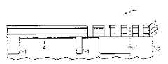
图1显示根据本发明方法制造的存储器件的半成品的表面部分的平面图。字线WLn被提供为平行地从左到右横跨存储单元阵列28区域延展。这一区域包括衬底或半导体本体的半导体材料中的浅沟槽隔离1,如虚线显示,它们彼此分开并平行设置,而且正交地横跨字线延展。位线设置在浅沟槽隔离1的区域上方并在此未示出。在浅沟槽隔离之间具有包括存储单元晶体管结构的有源区。FIG. 1 shows a plan view of a surface portion of a semi-finished product of a memory device manufactured according to the method of the invention. Word linesWLn are provided extending in parallel across the
通过本发明方法制造的优选实施例包括设置在图1阴影区域中的导电局部互连2。每一个局部互连2跨越浅沟槽隔离1并且连接以一个正方形设置的四个相邻的存储单元的源/漏区。存储单元的晶体管结构的沟道区位于该局部互连的末端部分下的源/漏区之间的附属字线下方。存储单元的源/漏区的位置以在图1中的存储单元e的例子示出,在此源/漏区通过S/D来表示。A preferred embodiment produced by the method of the invention comprises an electrically conductive
如果通过连续计数沿着字线列举存储单元,则局部互连将各自字线的一侧上的奇数存储单元的源/漏区连接到随后的偶数存储单元的源/漏区。根据该连续计数,在同一字线的另一侧,局部互连将偶数存储单元的源/漏区连接到随后的奇数存储单元。由于局部互连2属于相邻的两字线中的存储单元,因此局部互连连接全部四个存储单元的源/漏区,它们以一个四元正方形(square quadruple)设置。例如,位于图1中的a、b、c和d的存储单元,通过图1中指定的局部互连L1连接,使得四个存储单元的每一个包括一个连接到在这一四元正方形的其它三个存储单元的源/漏区的源/漏区。If memory cells are enumerated along a word line by consecutive counting, local interconnects connect the source/drain regions of odd memory cells on one side of the respective word line to the source/drain regions of subsequent even memory cells. On the other side of the same word line, local interconnects connect the source/drain regions of even memory cells to subsequent odd memory cells according to this consecutive count. Since the
存储器件进一步包括外围寻址,设置CMOS器件以形成电路作为在读、写和擦除操作中寻址存储单元的逻辑电路。这些电路的互补晶体管根据标准技术制造,但制造步骤结合在本发明的方法中,它允许制造具有集成CMOS寻址电路的超小尺寸的电荷捕获存储单元阵列。作为例子,图1显示出晶体管结构包括用来控制包括LDD(轻掺杂漏)区21的源/漏区20之间的沟道区的栅电极26。存储单元阵列28的区域通常与包括CMOS器件的外围区域29分离,它根据包括半导体衬底中用于互补晶体管的p-阱和n-阱设置的标准技术来处理。The memory device further includes peripheral addressing, a CMOS device arranged to form a circuit as logic for addressing memory cells during read, write and erase operations. The complementary transistors of these circuits are fabricated according to standard techniques, but the fabrication steps are combined in the method of the present invention, which allows fabrication of ultra-small size arrays of charge trapping memory cells with integrated CMOS addressing circuitry. As an example, FIG. 1 shows a transistor structure comprising a
图2显示参考图8定向的沿着虚线插入图1中的半成品的截面图。在右手侧,该截面显示在两个不同参考平面的存储单元阵列区域。波浪线左侧,显示通过浅沟槽隔离1区域的截面,而在波浪线的右侧,显示有源区的截面。浅沟槽隔离1通过在半导体材料中蚀刻沟槽和之后在沟槽中填充优选为氧化物的电介质材料的的标准方式来产生。氧化栅4设置在半导体本体3的上表面。对于将要制造的不同晶体管类型,可以改变氧化栅4的厚度和材料。根据在半导体本体的不同区域中的不同的晶体管类型对阱进行注入和退火。FIG. 2 shows a cross-sectional view of the semi-finished product inserted in FIG. 1 , oriented with reference to FIG. 8 , along the dotted line. On the right-hand side, the cross section shows the memory cell array region at two different reference planes. To the left of the wavy line, a cross-section through the
之后,在半导体本体的上表面施加为字线叠层提供的层排列。该层排列优选包括优选为多晶硅的栅电极层5,用来降低字线的电布线电阻且优选使用金属或金属硅化物制造的字线层6,和硬掩模层7,其优选为氮化物。通过后续的光刻和蚀刻步骤,构造该栅电极层5、该字线层6和该硬掩模层7以在用于存储单元阵列28的区域中形成平行的字线叠层。为全面起见,图2示出中间叠层,其横向尺寸不同于字线宽度的固定间距和字线之间的间隙,并且由于光刻步骤中出现的边界效应,该叠层位于存储单元阵列28的区域和CMOS外围区域29之间的过渡区域中。Afterwards, the layer arrangement provided for the word line stack is applied to the upper surface of the semiconductor body. The layer arrangement preferably comprises a
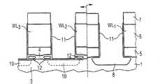
图3显示根据图2在湿法蚀刻工艺步骤在氧化栅4中形成蚀刻开口8和在存储单元阵列28的区域中中形成浅沟槽隔离1之后的截面图。在图3中显示,蚀刻浅沟槽隔离1的氧化物材料,深度通常约20到30nm,即比氧化栅4略深。蚀刻开口8在栅电极层5和栅电极层5的底部横向边缘处的半导体本体3之间形成底切开口。图3示出和图1的平面图比较的字线WL1、WL2、WL3和WL4的字线叠层。3 shows a cross-sectional view according to FIG. 2 after forming
图4示出根据图3的进一步工艺步骤之后的截面图,通过其制造存储层排列,特别是电荷捕获层排列。进一步描述用于包括ONO存储层排列的优选实施例的本发明的方法的优选例子,尽管也可以使用适合于电荷捕获存储单元的任何材料排列。FIG. 4 shows a sectional view after the further process step according to FIG. 3 , by which a storage layer arrangement, in particular a charge trapping layer arrangement, is produced. A preferred example of the method of the invention is further described for a preferred embodiment comprising an arrangement of ONO memory layers, although any arrangement of materials suitable for a charge trapping memory cell may also be used.
准备底部限制层,在氧化物-氮化物-氧化物电荷捕获层排列的情况下其为氧化层。通过结合半导体材料的热氧化和高温氧化物的沉积至通常大约4nm的厚度来制造底部限制层。随后用LPCVD(低压化学气相沉积)方式沉积厚度大约4nm的氮化层,通过其在栅电极层和半导体材料之间的底切开口中制造作为电荷存储的实际位置的存储层。然后,通过注入掺杂原子如硼或砷来形成源/漏区。在退火源/漏注入之后,湿法蚀刻沉积的氮化物以使得以提供的尺寸保持存储层。A bottom confinement layer is prepared, which is an oxide layer in the case of an oxide-nitride-oxide charge trapping layer arrangement. The bottom confinement layer is fabricated by a combination of thermal oxidation of the semiconductor material and deposition of a high temperature oxide to a thickness typically around 4 nm. A nitride layer with a thickness of approximately 4 nm is subsequently deposited by means of LPCVD (low pressure chemical vapor deposition), by means of which a storage layer is produced in the undercut opening between the gate electrode layer and the semiconductor material as the actual location of the charge storage. Then, source/drain regions are formed by implanting dopant atoms such as boron or arsenic. After annealing the source/drain implants, the deposited nitride is wet etched to maintain the memory layer at the provided dimensions.
描述的利用底切开口的工艺步骤形成包括只有几纳米宽度并尤其适合小尺寸和极短沟道的多位存储单元的条状部分的存储器层,这是因为它们在存储位的位置之间提供充分的电分离。但是,如上所述,它具有以标准方式形成并且在沟道的中间部分上不间断的电荷捕获层。The described process steps using undercut openings form a memory layer comprising strips of multi-bit memory cells that are only a few nanometers wide and are especially suitable for small dimensions and very short channels, since they are between the locations where the bits are stored Provides sufficient electrical separation. However, as mentioned above, it has a charge trapping layer formed in a standard manner and uninterrupted over the middle part of the channel.
图4示出源/漏区10和存储层12的位置。在该实施例的每一个字线叠层中,存储层12由沿着栅电极层5的底部边缘延展的两条带组成。再氧化该结构表面以在字线叠层的侧壁上形成薄氧化层。通过沉积优选为氧化物的间隙填充物9来填充字线叠层之间的间隙,之后对其进行平坦化,例如通过CMP(化学机械抛光)。在通过硬掩模层7形成的平坦表面和平坦化的间隙填充物9之后,沉积优选为氮化硅的盖层。FIG. 4 shows the positions of the source/
图5示出根据图4参考图7的取向沿着图1插入中的虚线的半成品放大截面图,其环绕第一个三字线WL1、WL2和WL3的字线叠层排列的区域。通过虚线指定的PN结示出源/漏区10的注入边界。示出在栅电极层5的底部边缘和半导体本体3之间的存储层12的条状部分的截面图。例如氮化物的存储层12嵌入在电介质材料中,电介质材料在ONO存储层排列的情况下为氧化材料且能作为氧化栅4的一部分。由再氧化层11覆盖字线叠层的侧壁。图5的右侧示出的有源区域之间的区域,在此蚀刻的开口8出现在浅沟槽隔离1的区域中。用优选为氧化硅的电介质材料的间隙填充物来填充字线之间的间隙,如上所述。5 shows an enlarged cross-sectional view of the semi-finished product along the dotted line in the inset of FIG.1 according to the orientation of FIG.4 with reference to FIG. . The implantation boundaries of the source/
图6示出根据图4在形成源/漏接触之后的截面图。平坦化步骤之后,优选为氮化物的盖层13被沉积并通过随后的光刻步骤被构造。在这一步骤中,在提供源/漏接触的区域中去除盖层13。如果盖层13是氮化物并且间隙填充物9是氧化物,则优选通过反应性离子蚀刻来构造盖层13。当到达间隙填充物9的氧化物时停止蚀刻工艺。在此之后,在间隙填充物9的材料中蚀刻出凹槽。这些凹槽的深度至少近似地对应于硬掩模14的厚度。然后沉积用于形成侧壁间隔物的材料。这些材料优选氮化物,其通过反应性离子蚀刻去除以在硬掩模层7的水平处的凹槽中形成通常30nm宽的第一间隔物14和在盖层13中的开口的侧壁上形成第二间隔物15。FIG. 6 shows a cross-sectional view according to FIG. 4 after forming source/drain contacts. After the planarization step, a
第一间隔物14与接下来的各向异性蚀刻工艺相关,通过其在源/漏区的区域中去除填充物9直到半导体材料的表面。由于蚀刻工艺为各向异性,所以第一间隔物14掩蔽字线叠层的侧壁上的间隙填充物9的材料以使得间隙填充材料残留物16留在这些侧壁上,形成字线的侧壁绝缘。本发明的方法的这一重要步骤提供字线的侧壁绝缘,该字线通常使用代替氮化物的氧化物形成,如通过描述的例子所显示的。然后导电材料例如多晶硅用来形成局部互连2,提供其作为源/漏接触和源/漏区与位线之间的电连接。The
存在根据沿着字线的要求尺寸构造局部互连2的不同的可能性。通过使用覆盖在字线叠层之间间隙的周期性间隔的区域的掩模来蚀刻间隙填充物9,使得间隙填充物9的材料留在这些区域中作为在蚀刻的孔之间的电绝缘,这些孔被用于局部互连的导电材料填充。但是,构造局部互连2的优选处理步骤顺序包括蚀刻间隙填充物9以在字线叠层之间开口的间隙中的间隙填充残留物16之间形成连续沟槽,其填充有作为局部互连的导电材料。然后,根据局部互连所需的纵向尺寸通过掩模和进一步的蚀刻处理来结构化该材料;并且在结构化的互连之间的间隙中再次填充电介质材料,其优选为氧化物。平坦化该局部互连材料。There are different possibilities of configuring the
图7示出根据图6的半成品的根据图5的放大截面图。在这个截面图中,详细的表示出间隙填充物9,再氧化层11,存储层12的设置,结构化的盖层13,第一间隔物14,第二间隔物15和间隙填充残留物16。第一间隔物14用于将间隙填充物9构造为间隙填充残留物16,该第一间隔物不必与第二间隔物15分开,如图6所示,但可以仅仅轻微的将它们分开。这一特征可根据具体情况变化。它的重要性仅仅在于具有第一间隔物14以掩蔽间隙填充物9的边缘部分,使得它们不会被蚀刻掉,而是形成字线叠层的侧壁绝缘。FIG. 7 shows an enlarged sectional view according to FIG. 5 of the semifinished product according to FIG. 6 . In this sectional view, the
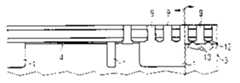
图8显示根据图6在进行以构造CMOS器件的进一步工艺步骤之后的截面图。在施加上部绝缘层17之后,其中上部绝缘层17可被沉积作为等离子加强的氮化物,被覆盖有抗反射涂层来辅助随后的光刻,通过在外围区域中蚀刻空隙18来构造CMOS器件。这一结构定义形成部分栅电极层5的栅电极。这显示于图8的左侧。在一标准的再氧化步骤之后,注入掺杂原子以形成LDD(轻掺杂漏区)区域21。沉积氮化物衬垫之后,宽的侧壁间隔物尤其是氧化物间隔物19形成在栅电极叠层的侧壁。这些侧壁间隔物19具有约150nm的典型宽度。然后侧壁间隔物19用作源/漏区注入的掩模以形成CMOS器件的源/漏区20。在该注入过程中LDD区域21被侧壁间隔物19覆盖。FIG. 8 shows a cross-sectional view according to FIG. 6 after further process steps performed to construct a CMOS device. After applying an upper insulating
CMOS器件之间的空隙18显著大于字线叠层之间的小间隙。通过本发明的方法,可制造在具有低至70nm尺寸的存储单元阵列中和具有需要使用较宽侧壁间隔物19的典型横向尺寸的CMOS器件结构中的两种晶体管结构。由于在外围区域29中栅叠层的高度,即衬底的垂直尺寸大于字线叠层的高度,所以空隙18必须相对宽于在存储单元区域28中的字线叠层之间的间隙。在本发明的结构的优选实施例中,当包括前述的层加上盖层13和绝缘材层17的栅极叠层的垂直尺寸d2至少是250nm时,包括栅电极层5、字线层6和硬掩模层7的字线叠层的垂直尺寸d1至多是200nm。存储单元阵列的横向间隔d3作为邻近的字线叠层的相应点之间的距离通过穿过字线叠层来测量,其被选择为至多250nm。因此,本发明的方法提供一系列的工艺步骤,其适合于在特别小尺寸中完全构造存储单元阵列之后,在具有适当尺寸的外围区域中制造电路的CMOS器件。以这种方式,可根据晶体管器件的类型选择适当的横向和垂直尺寸。描述的层排列和工艺步骤的顺序尤其适合于制造完全集成的存储器件。The
图9显示在外围区域29中应用源/漏接触之后图8的截面图。在结注入的退火之后,去除了侧壁间隔物19,例如通过湿法蚀刻。然后用电介质材料填充空隙18,电介质材料可以包括根据标准技术沉积的氧化物和氮化物层以及主要间隙填充物BPSG(硼磷硅化玻璃)。尤其在存储单元阵列28的区域中,这些填充物形成用于金属化级布线的基本电介质22。图9显示在邻近第一字线WL1的局部互连2上具有位线接触24的位线23。位线23和位线接触24可通过已知的名为双镶嵌工艺来制造。接下来用电导材料填充的接触孔用于产生将被连接的CMOS器件的源/漏区上的漏接触通孔25。CMOS器件的栅电极26也可以通过栅电极通孔27来接触。当栅电极26还可以通过适当的结构化栅电极层5的一部分被电连接时,例如图1中显示的那样,在图9中栅接触通孔27用虚线表示。进一步的金属布线层和金属间氧化物以通常的方式施加,并没有显示在图9中。然后该存储器件以包括钝化和掩蔽(housing)工艺的标准完成工艺步骤进一步处理。由于这不是本发明的方法的构成部分,所以没有详细地描述。FIG. 9 shows the cross-sectional view of FIG. 8 after application of source/drain contacts in the
电荷捕获存储单元的存储单元阵列的一个优选实施例包括具有SiGe层的改进的栅极结构。该结构通过如图10到13的截面中显示的优选制造方法进一步详细描述。A preferred embodiment of a memory cell array of charge trapping memory cells includes an improved gate structure with a SiGe layer. The structure is described in further detail by a preferred fabrication method as shown in cross section in FIGS. 10 to 13 .
图10的截面显示半导体本体3,它被提供有浅沟槽隔离1以分开存储单元的列。在存储单元阵列的区域中的半导体本体3的表面覆盖有氧化栅4,其优选通过热生长形成,典型厚度大约4nm。施加SiGe层30,之后沉积栅电极层5,优选多晶硅,金属和/或金属硅化物的字线层6,例如包括钨,和硬掩模层7。SiGe层优选是10nm到15nm厚和优选包含20原子百分比和70原子百分比之间的锗。结构化字线叠层,包括SiGe层30,其形成字线叠层的一部分。然后,各向同性和有选择地回蚀刻SiGe层30至栅电极层5和氧化栅4的材料。The cross-section of Fig. 10 shows a
如果栅电极层是多晶硅和氧化栅是二氧化硅,则可进行蚀刻步骤,例如,通过下列变化中的一种。第一种变化使用多晶硅蚀刻剂,由70%的HNO3,49%的HF,99.9%的CH3COOH和水构成。在相对原子量中,组分比例例如是40∶1∶2∶57。为10∶1到10∶5之间的典型比率的混合物优选在水中溶解(参见,例如S.M.Kim等人的IEEE学报的纳米技术2,第253页,(2003))。第二种变化在典型温度90℃下使用30%的H2O2,如果锗比例高,典型地大于60%,这尤其适合(参见,例如A.Franke等人的微电机械系统杂志12,4月,2003)。第三种变化使用由30%的NH4OH,30%的H2O2和水,在典型温度75℃下的优选比例1∶1∶5构成的蚀刻剂。使用这种蚀刻剂,获得接下来的选择性蚀刻,根据F.Scott Johnson等人的电子材料杂志21,第805-810页(1992):对于包含40原子百分比的锗的SiGe;SiGe的蚀刻率和Si的蚀刻率的比为36∶1并且SiGe的蚀刻率和SiO2的蚀刻率的比是100∶1;对于包含55原子百分比的锗的SiGe∶SiGe的蚀刻率和Si的蚀刻率的比为177∶1并且SiGe的蚀刻率和SiO2的蚀刻率的比是487∶1。由于SiGe对于Si和SiO2的超过100∶1的选择性可通过这些湿法蚀刻的方法获得,所以浅沟槽隔离1的氧化物的底部蚀刻可以避免。If the gate electrode layer is polysilicon and the gate oxide is silicon dioxide, the etching step may be performed, for example, by one of the following variations. The first variation uses a polysilicon etchant consisting of 70%HNO3 , 49% HF, 99.9%CH3COOH and water. In relative atomic weights, the component ratio is, for example, 40:1:2:57. Mixtures in typical ratios between 10:1 and 10:5 are preferably dissolved in water (see eg SM Kim et al. IEEE Transactions on
在图11的截面中显示SiGe层30的该蚀刻工艺获得的半成品的结果。在字线叠层和半导体本体之间的SiGe层中具有横向凹槽,在栅电极层5和氧化栅4之间留下SiGe层30的残留物部分。然后各向同性蚀刻氧化栅4,例如通过HF。由于从上面的垂直方向的蚀刻腐蚀,几乎没有去除浅沟槽隔离1的氧化物;如果需要,可加入润湿剂。The result of this etching process of the
图12显示将除了SiGe层30的残留部分下面的保留部分之外的氧化栅去除之后的下一半成品。然后,优选为热生长SiO2的另一电介质材料产生在半导体材料、SiGe层、氧化栅层5的自由表面上。FIG. 12 shows the next semi-finished product after removal of the gate oxide except for the remaining portion below the remaining portion of the
该再氧化层11显示在附图13的截面图中,其也显示接下来施加的用于存储层12的材料层。优选为Si3N4,其通过低压化学气相沉积可以共形地施加。为存储层12提供的横向凹槽具有由于制造再氧化层11引起的轻微减小的尺寸。用作存储层12的材料层优选沉积至少为所述凹槽尺寸的一半厚。在上述的典型尺寸的情况下,该层厚度优选约5nm。以这种方式,材料完全填充凹槽以使得存储层12能形成为整体的纳米条。层的厚度没有按比例画出。在SiGe层的横向表面上的再氧化层厚度典型为约4nm,但是,在这个例子中,在字线叠层的侧壁上典型地生长约6nm的厚度。这是由于栅电极层5的多晶硅的高掺杂的缘故。This
然后各向同性地回蚀刻包括存储层材料的层,以使得残留物部分被留下,形成存储层12。由于浅沟槽隔离没有被底部蚀刻,因此获得具有纳米范围内的宽度的薄连续条的存储层12。接着,可以注入源/漏区的掺杂,根据已经描述的实施例的侧壁间隔物16可通过通常的共形沉积和各向异性蚀刻来形成。The layer comprising the storage layer material is then isotropically etched back so that a residue portion is left, forming the
尽管本发明及其优势已经详细描述,但应当理解在此在不脱离本发明精神和通过附加的权利要求限定的本发明保护范围的情况下来制作各种变化,替代和转化。Although the present invention and its advantages have been described in detail, it should be understood that various changes, substitutions and alterations can be made herein without departing from the spirit and scope of the invention as defined by the appended claims.
附图标记表Table of reference signs
1 浅沟槽隔离1 shallow trench isolation
2 局部互连2 local interconnect
3 半导体本体3 semiconductor body
4 氧化栅4 oxide grid
5 栅电极层5 Gate electrode layer
6 字线层6 word line layer
7 硬掩模层7 hard mask layer
8 蚀刻开口8 Etched openings
9 间隙填充物9 Gap filler
10 源/漏区10 source/drain area
11 再氧化层11 reoxidation layer
12 存储层12 storage tiers
13 盖层13 cover layer
14 第一间隔物14 first spacer
15 第二间隔物15 second spacer
16 间隙填充残留物16 Gap Fill Residue
17 绝缘层17 insulation layer
18 空隙18 gaps
19 侧壁间隔物19 sidewall spacers
20 源/漏区20 source/drain area
21 LDD区21 LDD District
22 基本电介质22 basic dielectric
23 位线23 bit line
24 位线接触24 bit line contact
25 漏接触通孔25 drain contact vias
26 栅电极26 Gate electrode
27 栅接触通孔27 gate contact vias
28 存储单元阵列28 memory cell array
29 外围区域29 outlying area
30 SiGe层30 SiGe layers
Claims (16)
Translated fromChineseApplications Claiming Priority (2)
| Application Number | Priority Date | Filing Date | Title |
|---|---|---|---|
| US11/061,314US7186607B2 (en) | 2005-02-18 | 2005-02-18 | Charge-trapping memory device and method for production |
| US11/061314 | 2005-02-18 |
Publications (2)
| Publication Number | Publication Date |
|---|---|
| CN1870249A CN1870249A (en) | 2006-11-29 |
| CN100405582Ctrue CN100405582C (en) | 2008-07-23 |
Family
ID=36794234
Family Applications (1)
| Application Number | Title | Priority Date | Filing Date |
|---|---|---|---|
| CNB2006100711051AExpired - Fee RelatedCN100405582C (en) | 2005-02-18 | 2006-02-17 | Charge trap memory device and manufacturing method thereof |
Country Status (3)
| Country | Link |
|---|---|
| US (1) | US7186607B2 (en) |
| CN (1) | CN100405582C (en) |
| DE (1) | DE102005012112B4 (en) |
Families Citing this family (20)
| Publication number | Priority date | Publication date | Assignee | Title |
|---|---|---|---|---|
| DE102005013982A1 (en)* | 2005-03-26 | 2006-10-05 | Atmel Germany Gmbh | A method of manufacturing a bipolar transistor and a bipolar transistor produced by such a method |
| US20070212832A1 (en)* | 2006-03-08 | 2007-09-13 | Freescale Semiconductor Inc. | Method for making a multibit transistor |
| KR100871754B1 (en)* | 2007-05-25 | 2008-12-05 | 주식회사 동부하이텍 | Manufacturing Method of Semiconductor Memory Device |
| JP5319092B2 (en)* | 2007-09-03 | 2013-10-16 | スパンション エルエルシー | Semiconductor device and manufacturing method thereof |
| JP5264139B2 (en)* | 2007-10-09 | 2013-08-14 | スパンション エルエルシー | Manufacturing method of semiconductor device |
| JP5313486B2 (en)* | 2007-11-15 | 2013-10-09 | スパンション エルエルシー | Manufacturing method of semiconductor device |
| JP5328145B2 (en)* | 2007-12-24 | 2013-10-30 | ラピスセミコンダクタ株式会社 | Nonvolatile memory device and manufacturing method thereof |
| US20100062593A1 (en)* | 2008-09-10 | 2010-03-11 | Promos Technologies Inc. | Method for preparing multi-level flash memory devices |
| US8314475B2 (en) | 2010-11-09 | 2012-11-20 | Hewlett-Packard Development Company, L.P. | Nanoscale electronic device with anisotropic dielectric material |
| KR20120131879A (en)* | 2011-05-26 | 2012-12-05 | 삼성전자주식회사 | Semiconductor device and method for manufacturing the same |
| US8698222B2 (en) | 2011-11-24 | 2014-04-15 | Macronix International Co., Ltd. | Memory device with charge storage layers at the gaps located both sides of the gate dielectric underneath the gate |
| US8674424B2 (en)* | 2011-11-24 | 2014-03-18 | Macronix International Co., Ltd. | Memory device with charge storage layers at the sidewalls of the gate and method for fabricating the same |
| TWI475670B (en)* | 2011-11-24 | 2015-03-01 | Macronix Int Co Ltd | Memory device and method of fabricating the same |
| CN103137627A (en)* | 2011-11-25 | 2013-06-05 | 旺宏电子股份有限公司 | Memory device and method of manufacturing the same |
| CN103515355A (en)* | 2012-06-29 | 2014-01-15 | 联华电子股份有限公司 | Semiconductor element and its manufacturing method |
| CN103839892B (en)* | 2012-11-26 | 2016-08-10 | 李迪 | A kind of semiconductor structure and manufacture method thereof |
| CN104037207A (en)* | 2013-03-07 | 2014-09-10 | 旺宏电子股份有限公司 | Memory device and method of manufacturing the same |
| US20150171181A1 (en)* | 2013-12-17 | 2015-06-18 | Macronix International Co., Ltd. | Ono structure with separated electron trapping |
| US10224235B2 (en)* | 2016-02-05 | 2019-03-05 | Lam Research Corporation | Systems and methods for creating airgap seals using atomic layer deposition and high density plasma chemical vapor deposition |
| CN115955839B (en)* | 2023-03-03 | 2023-06-02 | 长鑫存储技术有限公司 | Semiconductor structure and preparation method thereof |
Citations (5)
| Publication number | Priority date | Publication date | Assignee | Title |
|---|---|---|---|---|
| US5768192A (en)* | 1996-07-23 | 1998-06-16 | Saifun Semiconductors, Ltd. | Non-volatile semiconductor memory cell utilizing asymmetrical charge trapping |
| US6011725A (en)* | 1997-08-01 | 2000-01-04 | Saifun Semiconductors, Ltd. | Two bit non-volatile electrically erasable and programmable semiconductor memory cell utilizing asymmetrical charge trapping |
| CN1446378A (en)* | 2000-08-11 | 2003-10-01 | 因芬尼昂技术股份公司 | Storage unit, storage unit device and manufacturing method |
| CN1449049A (en)* | 2002-03-29 | 2003-10-15 | 旺宏电子股份有限公司 | A non-volatile semiconductor memory unit with electron trapping erased state and its operation method |
| CN1531107A (en)* | 2003-03-17 | 2004-09-22 | ���ǵ�����ʽ���� | Flash memory having local SONOS structure using undercut gate and method of fabricating the same |
Family Cites Families (15)
| Publication number | Priority date | Publication date | Assignee | Title |
|---|---|---|---|---|
| DE19924439A1 (en)* | 1999-05-28 | 2000-11-30 | Bayer Ag | Fast cross-linking fluoropolymer |
| US6548881B1 (en) | 2000-07-25 | 2003-04-15 | Advanced Micro Devices, Inc. | Method and apparatus to achieve bond pad crater sensing and stepping identification in integrated circuit products |
| JP4904631B2 (en) | 2000-10-27 | 2012-03-28 | ソニー株式会社 | Nonvolatile semiconductor memory device and manufacturing method thereof |
| JP2002198446A (en)* | 2000-12-27 | 2002-07-12 | Fujitsu Ltd | Semiconductor memory device and manufacturing method thereof |
| DE10110150A1 (en)* | 2001-03-02 | 2002-09-19 | Infineon Technologies Ag | Method for producing metallic bit lines for memory cell arrays, method for producing memory cell arrays and memory cell array |
| US6580120B2 (en)* | 2001-06-07 | 2003-06-17 | Interuniversitair Microelektronica Centrum (Imec Vzw) | Two bit non-volatile electrically erasable and programmable memory structure, a process for producing said memory structure and methods for programming, reading and erasing said memory structure |
| DE10129958B4 (en)* | 2001-06-21 | 2006-07-13 | Infineon Technologies Ag | Memory cell arrangement and manufacturing method |
| JP3873679B2 (en)* | 2001-07-23 | 2007-01-24 | セイコーエプソン株式会社 | Semiconductor capacitance device, booster circuit, and nonvolatile semiconductor memory device |
| US6743674B2 (en) | 2001-09-18 | 2004-06-01 | Silicon Storage Technology, Inc. | Method of forming a semiconductor array of floating gate memory cells and strap regions, and a memory array and strap regions made thereby |
| JP2003258128A (en)* | 2002-02-27 | 2003-09-12 | Nec Electronics Corp | Nonvolatile semiconductor memory device, method of manufacturing the same, and method of operating the same |
| US6777725B2 (en)* | 2002-06-14 | 2004-08-17 | Ingentix Gmbh & Co. Kg | NROM memory circuit with recessed bitline |
| US6570211B1 (en)* | 2002-06-26 | 2003-05-27 | Advanced Micro Devices, Inc. | 2Bit/cell architecture for floating gate flash memory product and associated method |
| US6734063B2 (en)* | 2002-07-22 | 2004-05-11 | Infineon Technologies Ag | Non-volatile memory cell and fabrication method |
| US7051492B2 (en)* | 2003-12-15 | 2006-05-30 | Illinois Tool Works Inc. | Film wrapping apparatus with negator spring biasing members |
| US7041545B2 (en) | 2004-03-08 | 2006-05-09 | Infineon Technologies Ag | Method for producing semiconductor memory devices and integrated memory device |
- 2005
- 2005-02-18USUS11/061,314patent/US7186607B2/ennot_activeExpired - Fee Related
- 2005-03-16DEDE102005012112Apatent/DE102005012112B4/ennot_activeExpired - Lifetime
- 2006
- 2006-02-17CNCNB2006100711051Apatent/CN100405582C/ennot_activeExpired - Fee Related
Patent Citations (5)
| Publication number | Priority date | Publication date | Assignee | Title |
|---|---|---|---|---|
| US5768192A (en)* | 1996-07-23 | 1998-06-16 | Saifun Semiconductors, Ltd. | Non-volatile semiconductor memory cell utilizing asymmetrical charge trapping |
| US6011725A (en)* | 1997-08-01 | 2000-01-04 | Saifun Semiconductors, Ltd. | Two bit non-volatile electrically erasable and programmable semiconductor memory cell utilizing asymmetrical charge trapping |
| CN1446378A (en)* | 2000-08-11 | 2003-10-01 | 因芬尼昂技术股份公司 | Storage unit, storage unit device and manufacturing method |
| CN1449049A (en)* | 2002-03-29 | 2003-10-15 | 旺宏电子股份有限公司 | A non-volatile semiconductor memory unit with electron trapping erased state and its operation method |
| CN1531107A (en)* | 2003-03-17 | 2004-09-22 | ���ǵ�����ʽ���� | Flash memory having local SONOS structure using undercut gate and method of fabricating the same |
Also Published As
| Publication number | Publication date |
|---|---|
| US7186607B2 (en) | 2007-03-06 |
| DE102005012112A1 (en) | 2006-08-31 |
| US20060186480A1 (en) | 2006-08-24 |
| DE102005012112B4 (en) | 2011-03-17 |
| CN1870249A (en) | 2006-11-29 |
Similar Documents
| Publication | Publication Date | Title |
|---|---|---|
| CN100405582C (en) | Charge trap memory device and manufacturing method thereof | |
| US9379120B2 (en) | Metal control gate structures and air gap isolation in non-volatile memory | |
| US8546239B2 (en) | Methods of fabricating non-volatile memory with air gaps | |
| US9123577B2 (en) | Air gap isolation in non-volatile memory using sacrificial films | |
| JP3917063B2 (en) | Semiconductor device and manufacturing method thereof | |
| JP5116294B2 (en) | Semiconductor structure and manufacturing method thereof (vertical SOI trench SONOS cell) | |
| JP4989630B2 (en) | Array source line in NAND flash memory | |
| US7230295B2 (en) | Nonvolatile memory cell with multiple floating gates formed after the select gate | |
| US6885044B2 (en) | Arrays of nonvolatile memory cells wherein each cell has two conductive floating gates | |
| US9123714B2 (en) | Metal layer air gap formation | |
| US7375387B2 (en) | Method for producing semiconductor memory devices and integrated memory device | |
| US20060128097A1 (en) | Nonvolatile memory cells with buried channel transistors | |
| US7960266B2 (en) | Spacer patterns using assist layer for high density semiconductor devices | |
| US8952536B2 (en) | Semiconductor device and method of fabrication | |
| US20130307044A1 (en) | Selective Air Gap Isolation In Non-Volatile Memory | |
| CN1979866B (en) | Storage device | |
| US7713875B2 (en) | Variable salicide block for resistance equalization in an array | |
| US20060001081A1 (en) | Nonvolatile semiconductor memory device and manufacturing method thereof | |
| US20070126028A1 (en) | Low resistance void-free contacts | |
| US7060565B2 (en) | Fabrication of dielectric for a nonvolatile memory cell having multiple floating gates | |
| US20140187032A1 (en) | Method for fabricating memory device | |
| TW200849563A (en) | NAND flash memory cell array and method of fabricating the same |
Legal Events
| Date | Code | Title | Description |
|---|---|---|---|
| C06 | Publication | ||
| PB01 | Publication | ||
| C10 | Entry into substantive examination | ||
| SE01 | Entry into force of request for substantive examination | ||
| C14 | Grant of patent or utility model | ||
| GR01 | Patent grant | ||
| C17 | Cessation of patent right | ||
| CF01 | Termination of patent right due to non-payment of annual fee | Granted publication date:20080723 |