CN100402694C - Integrated circuit devices and fabrication using metal-doped chalcogenide materials - Google Patents
Integrated circuit devices and fabrication using metal-doped chalcogenide materialsDownload PDFInfo
- Publication number
- CN100402694C CN100402694CCNB028214501ACN02821450ACN100402694CCN 100402694 CCN100402694 CCN 100402694CCN B028214501 ACNB028214501 ACN B028214501ACN 02821450 ACN02821450 ACN 02821450ACN 100402694 CCN100402694 CCN 100402694C
- Authority
- CN
- China
- Prior art keywords
- electrode
- plasma
- chalcogenide
- layer
- chalcogenide layer
- Prior art date
- Legal status (The legal status is an assumption and is not a legal conclusion. Google has not performed a legal analysis and makes no representation as to the accuracy of the status listed.)
- Expired - Lifetime
Links
Images


Classifications
- C—CHEMISTRY; METALLURGY
- C23—COATING METALLIC MATERIAL; COATING MATERIAL WITH METALLIC MATERIAL; CHEMICAL SURFACE TREATMENT; DIFFUSION TREATMENT OF METALLIC MATERIAL; COATING BY VACUUM EVAPORATION, BY SPUTTERING, BY ION IMPLANTATION OR BY CHEMICAL VAPOUR DEPOSITION, IN GENERAL; INHIBITING CORROSION OF METALLIC MATERIAL OR INCRUSTATION IN GENERAL
- C23C—COATING METALLIC MATERIAL; COATING MATERIAL WITH METALLIC MATERIAL; SURFACE TREATMENT OF METALLIC MATERIAL BY DIFFUSION INTO THE SURFACE, BY CHEMICAL CONVERSION OR SUBSTITUTION; COATING BY VACUUM EVAPORATION, BY SPUTTERING, BY ION IMPLANTATION OR BY CHEMICAL VAPOUR DEPOSITION, IN GENERAL
- C23C14/00—Coating by vacuum evaporation, by sputtering or by ion implantation of the coating forming material
- C23C14/06—Coating by vacuum evaporation, by sputtering or by ion implantation of the coating forming material characterised by the coating material
- C23C14/14—Metallic material, boron or silicon
- C23C14/18—Metallic material, boron or silicon on other inorganic substrates
- C—CHEMISTRY; METALLURGY
- C23—COATING METALLIC MATERIAL; COATING MATERIAL WITH METALLIC MATERIAL; CHEMICAL SURFACE TREATMENT; DIFFUSION TREATMENT OF METALLIC MATERIAL; COATING BY VACUUM EVAPORATION, BY SPUTTERING, BY ION IMPLANTATION OR BY CHEMICAL VAPOUR DEPOSITION, IN GENERAL; INHIBITING CORROSION OF METALLIC MATERIAL OR INCRUSTATION IN GENERAL
- C23C—COATING METALLIC MATERIAL; COATING MATERIAL WITH METALLIC MATERIAL; SURFACE TREATMENT OF METALLIC MATERIAL BY DIFFUSION INTO THE SURFACE, BY CHEMICAL CONVERSION OR SUBSTITUTION; COATING BY VACUUM EVAPORATION, BY SPUTTERING, BY ION IMPLANTATION OR BY CHEMICAL VAPOUR DEPOSITION, IN GENERAL
- C23C14/00—Coating by vacuum evaporation, by sputtering or by ion implantation of the coating forming material
- C23C14/58—After-treatment
- C23C14/5846—Reactive treatment
- C—CHEMISTRY; METALLURGY
- C23—COATING METALLIC MATERIAL; COATING MATERIAL WITH METALLIC MATERIAL; CHEMICAL SURFACE TREATMENT; DIFFUSION TREATMENT OF METALLIC MATERIAL; COATING BY VACUUM EVAPORATION, BY SPUTTERING, BY ION IMPLANTATION OR BY CHEMICAL VAPOUR DEPOSITION, IN GENERAL; INHIBITING CORROSION OF METALLIC MATERIAL OR INCRUSTATION IN GENERAL
- C23C—COATING METALLIC MATERIAL; COATING MATERIAL WITH METALLIC MATERIAL; SURFACE TREATMENT OF METALLIC MATERIAL BY DIFFUSION INTO THE SURFACE, BY CHEMICAL CONVERSION OR SUBSTITUTION; COATING BY VACUUM EVAPORATION, BY SPUTTERING, BY ION IMPLANTATION OR BY CHEMICAL VAPOUR DEPOSITION, IN GENERAL
- C23C14/00—Coating by vacuum evaporation, by sputtering or by ion implantation of the coating forming material
- C23C14/06—Coating by vacuum evaporation, by sputtering or by ion implantation of the coating forming material characterised by the coating material
- C23C14/0623—Sulfides, selenides or tellurides
- C—CHEMISTRY; METALLURGY
- C23—COATING METALLIC MATERIAL; COATING MATERIAL WITH METALLIC MATERIAL; CHEMICAL SURFACE TREATMENT; DIFFUSION TREATMENT OF METALLIC MATERIAL; COATING BY VACUUM EVAPORATION, BY SPUTTERING, BY ION IMPLANTATION OR BY CHEMICAL VAPOUR DEPOSITION, IN GENERAL; INHIBITING CORROSION OF METALLIC MATERIAL OR INCRUSTATION IN GENERAL
- C23C—COATING METALLIC MATERIAL; COATING MATERIAL WITH METALLIC MATERIAL; SURFACE TREATMENT OF METALLIC MATERIAL BY DIFFUSION INTO THE SURFACE, BY CHEMICAL CONVERSION OR SUBSTITUTION; COATING BY VACUUM EVAPORATION, BY SPUTTERING, BY ION IMPLANTATION OR BY CHEMICAL VAPOUR DEPOSITION, IN GENERAL
- C23C14/00—Coating by vacuum evaporation, by sputtering or by ion implantation of the coating forming material
- C23C14/22—Coating by vacuum evaporation, by sputtering or by ion implantation of the coating forming material characterised by the process of coating
- C23C14/54—Controlling or regulating the coating process
- C23C14/542—Controlling the film thickness or evaporation rate
- C23C14/544—Controlling the film thickness or evaporation rate using measurement in the gas phase
- H—ELECTRICITY
- H10—SEMICONDUCTOR DEVICES; ELECTRIC SOLID-STATE DEVICES NOT OTHERWISE PROVIDED FOR
- H10B—ELECTRONIC MEMORY DEVICES
- H10B63/00—Resistance change memory devices, e.g. resistive RAM [ReRAM] devices
- H10B63/20—Resistance change memory devices, e.g. resistive RAM [ReRAM] devices comprising selection components having two electrodes, e.g. diodes
- H—ELECTRICITY
- H10—SEMICONDUCTOR DEVICES; ELECTRIC SOLID-STATE DEVICES NOT OTHERWISE PROVIDED FOR
- H10N—ELECTRIC SOLID-STATE DEVICES NOT OTHERWISE PROVIDED FOR
- H10N70/00—Solid-state devices having no potential barriers, and specially adapted for rectifying, amplifying, oscillating or switching
- H10N70/011—Manufacture or treatment of multistable switching devices
- H10N70/041—Modification of switching materials after formation, e.g. doping
- H10N70/046—Modification of switching materials after formation, e.g. doping by diffusion, e.g. photo-dissolution
- H—ELECTRICITY
- H10—SEMICONDUCTOR DEVICES; ELECTRIC SOLID-STATE DEVICES NOT OTHERWISE PROVIDED FOR
- H10N—ELECTRIC SOLID-STATE DEVICES NOT OTHERWISE PROVIDED FOR
- H10N70/00—Solid-state devices having no potential barriers, and specially adapted for rectifying, amplifying, oscillating or switching
- H10N70/20—Multistable switching devices, e.g. memristors
- H10N70/24—Multistable switching devices, e.g. memristors based on migration or redistribution of ionic species, e.g. anions, vacancies
- H10N70/245—Multistable switching devices, e.g. memristors based on migration or redistribution of ionic species, e.g. anions, vacancies the species being metal cations, e.g. programmable metallization cells
- H—ELECTRICITY
- H10—SEMICONDUCTOR DEVICES; ELECTRIC SOLID-STATE DEVICES NOT OTHERWISE PROVIDED FOR
- H10N—ELECTRIC SOLID-STATE DEVICES NOT OTHERWISE PROVIDED FOR
- H10N70/00—Solid-state devices having no potential barriers, and specially adapted for rectifying, amplifying, oscillating or switching
- H10N70/801—Constructional details of multistable switching devices
- H10N70/821—Device geometry
- H10N70/826—Device geometry adapted for essentially vertical current flow, e.g. sandwich or pillar type devices
- H—ELECTRICITY
- H10—SEMICONDUCTOR DEVICES; ELECTRIC SOLID-STATE DEVICES NOT OTHERWISE PROVIDED FOR
- H10N—ELECTRIC SOLID-STATE DEVICES NOT OTHERWISE PROVIDED FOR
- H10N70/00—Solid-state devices having no potential barriers, and specially adapted for rectifying, amplifying, oscillating or switching
- H10N70/801—Constructional details of multistable switching devices
- H10N70/881—Switching materials
- H10N70/882—Compounds of sulfur, selenium or tellurium, e.g. chalcogenides
- H10N70/8825—Selenides, e.g. GeSe
Landscapes
- Chemical & Material Sciences (AREA)
- Engineering & Computer Science (AREA)
- Chemical Kinetics & Catalysis (AREA)
- Materials Engineering (AREA)
- Mechanical Engineering (AREA)
- Metallurgy (AREA)
- Organic Chemistry (AREA)
- Manufacturing & Machinery (AREA)
- Inorganic Chemistry (AREA)
- Semiconductor Memories (AREA)
- Physical Vapour Deposition (AREA)
- Inks, Pencil-Leads, Or Crayons (AREA)
Abstract
Description
Translated fromChinese本发明技术领域Technical Field of the Invention
本发明一般涉及集成电路存储器,尤其涉及在硫族化物存储元件和含该存储元件的集成电路器件的制造中对硫族化物材料掺杂金属。The present invention relates generally to integrated circuit memories, and more particularly to doping chalcogenide materials with metals in the fabrication of chalcogenide memory elements and integrated circuit devices incorporating the memory elements.
发明背景Background of the invention
电子可编程和可擦除材料,即在一般电阻状态和一般导电状态间可电子切换的材料,是本领域众所周知的。硫族化物材料是发现这些材料可用于半导体工业,尤其可用于制造非易失性存储器件的一个实例。Electronically programmable and erasable materials, ie, materials that are electronically switchable between a generally resistive state and a generally conductive state, are well known in the art. Chalcogenide materials are one example of such materials that find use in the semiconductor industry, especially in the fabrication of non-volatile memory devices.
硫族化物材料是由一种或更多种硫族元素和一种或更多种比硫族元素正电性更高的元素组成的化合物。硫族元素是通用IUPAC版周期表的VIB族元素,即氧(O)、硫(S)、硒(Se)、碲(Te)和钋(Po)。更高正电性的元素一般选自IVB和VB族。用于非易失性存储器的典型组合,包括硒及/或碲与锗(Ge)及/或锑(Sb)。但是,其它的组合也是已知的,如砷(As)和硫的组合。Chalcogenide materials are compounds composed of one or more chalcogen elements and one or more elements that are more electropositive than the chalcogen elements. Chalcogens are elements in group VIB of the common IUPAC version of the periodic table, namely oxygen (O), sulfur (S), selenium (Se), tellurium (Te) and polonium (Po). More electropositive elements are generally selected from groups IVB and VB. Typical combinations for non-volatile memory include selenium and/or tellurium with germanium (Ge) and/or antimony (Sb). However, other combinations are also known, such as arsenic (As) and sulfur.
为获得所需电特性,通常对硫族化物材料掺杂金属,如铜(Cu),银(Ag)、金(Au)或铝(Al)。图IA-ID描述了简单硫族化物存储元件100的制造。硫族化物存储元件的基本结构包括第一电极、第二电极和插在第一和第二电极之间的硫族化物材料。硫族化物存储器的另外细节,以及对硫族化物存储元件基本结构的变异实例,均在Wolstenholme等人1999年12月7日颁布的US 5,998,244,Reinberg 1999年7月6日颁布的US 5,920,788和Sandhu等人1998年11月17日颁布的US5,837,564中给出,各专利均由本公开的专利受让人共同转让。一般说来,硫族化物存储元件是在半导体晶片(wafer)或其它基片上形成的作为集成电路器件的一个部分。Chalcogenide materials are often doped with metals, such as copper (Cu), silver (Ag), gold (Au) or aluminum (Al), to obtain desired electrical properties. 1A-ID depict the fabrication of a simple
硫族化物存储元件一般存储一个位(single bit),如低电阻率(高导电率)相当于第一逻辑状态,高电阻率(低导电率)相当于第二逻辑状态。利用本领域众所周知的电流传感(sensing)技术同时施加一个低于阈电压的读取电位,读出硫族化物存储元件的不同水平电阻率。Chalcogenide memory elements generally store a single bit, for example, low resistivity (high conductivity) corresponds to the first logic state, and high resistivity (low conductivity) corresponds to the second logic state. Different levels of resistivity of the chalcogenide memory element are read using current sensing techniques well known in the art while applying a read potential below the threshold voltage.
在导电态之间,通过对掺杂后的硫族化物材料施加不同电场,可以电切换硫族化物存储元件。通过施加高于某一阈电压的可编程序电位,可以认为该金属掺合剂原子定位于树状结构中,从而形成导电通道,并降低该硫族化物材料的电阻率。施加反向极性的电位,这种转换是可逆的。可以施加其大小低于阈电压的外加电位范围,即读取电位,而不致改变该掺杂后的硫族化物材料的电阻率。可以把这些读取电位施加给该硫族化物存储元件,以读出该掺杂后的硫族化物材料的电阻率,并因此读出该存储元件的数据值。Between conductive states, the chalcogenide memory element can be electrically switched by applying different electric fields to the doped chalcogenide material. By applying a programmable potential above a certain threshold voltage, the metal dopant atoms are thought to localize in a dendritic structure, thereby forming conductive channels and reducing the resistivity of the chalcogenide material. This conversion is reversible by applying a potential of opposite polarity. A range of applied potentials whose magnitude is below the threshold voltage, ie read potential, can be applied without changing the resistivity of the doped chalcogenide material. The read potentials can be applied to the chalcogenide memory element to read the resistivity of the doped chalcogenide material, and thus the data value of the memory element.
不同于动态随机存取存储(DRAM)器件,为维持其编程状态,非易失性存储器件不要求定期恢愎。反而,非易失性存储器件可以被长时间(通常以年记)切断与电源的连接,而不致损失写入其存储单元(memory cells)中的信息。因此,最适用于非易失性存储器件的硫族化物材料将倾向于无限维持其电阻率的数值,只要外加电压不超过阈电压。Unlike dynamic random access memory (DRAM) devices, non-volatile memory devices do not require periodic refreshes in order to maintain their programmed state. In contrast, nonvolatile memory devices can be disconnected from power for long periods of time (usually in years) without losing information written to their memory cells. Therefore, chalcogenide materials most suitable for use in non-volatile memory devices will tend to maintain their resistivity values indefinitely as long as the applied voltage does not exceed the threshold voltage.
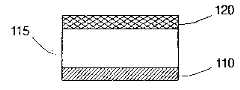
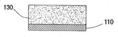
图1A中构成了第一电极110,构成硫族化物层115覆盖在第一电极110上。如前所述,硫族化物层115的电特性可通过对硫族化物材料掺杂金属而得以改善。这一般是通过一种由光子诱发金属原子扩散的被称为光致掺杂(photo-doping)方法完成的。在这个方法中,使金属层120首先形成在硫族化物层115上,如图1A所示。金属层120一般含铜、银、金、铝或其它高扩散金属。形成第一电极110及/或金属层120一般是在真空室中完成的,如采用真空溅射方法。In FIG. 1A , a
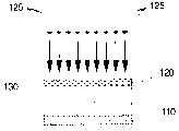
为使图1B中的光致掺杂过程继续,将电磁辐射125对准金属层120,使金属原子从金属层120扩散进入硫族化物层115。电磁辐射125一般是紫外(UV)光。驱使金属原子进入硫族化物层115导致形成内含硫族化物材料和扩散金属的掺杂后的硫族化物层130。为使该晶片表面曝露于紫外光源下,一般必须从真空室取出这种半导体晶片。To continue the photodoping process in FIG. 1B ,
光致掺杂过程一般进行至金属层120完全扩散进入掺杂后的硫族化物层130为止,如图1C所示。应该选择金属层120的厚度,使之可以达到在掺杂后的硫族化物层130中所需的掺杂水平。但是,金属层120必须足够地薄,如数百埃,以使电磁辐射125透射,构成所需的光子诱发的金属扩散。然后,如图1D所示,构成第二电极150,覆盖在掺杂后的硫族化物层130和金属层120的所有其余部分上,形成硫族化物存储元件100。如同第一电极110及/或硫族化物层115,一般也是在真空室中构成第二电极150。第二电极150优选是一种功函数(
这种传统光致掺杂方法有好几个缺点。这种方法可能费时,因为在上述各处理阶段的过程中要把半导体晶片移进和移出真空室。在各种工艺设备中对半导体晶片的这种移动也增加了传输过程中污染或其它损害的几率。此外,由于为了使光子有效地诱发金属扩散,该金属层必须薄,而所需的掺杂量可能不是用单一光致掺杂方法可有效达到的,因为这种必需的金属层厚度会导致电磁辐射过多反射。This conventional photodoping method has several disadvantages. This method can be time consuming because the semiconductor wafer is moved into and out of the vacuum chamber during the various processing stages described above. This movement of semiconductor wafers among the various process tools also increases the chances of contamination or other damage during transport. In addition, since the metal layer must be thin in order for photons to efficiently induce metal diffusion, the required doping level may not be effectively achievable with a single photo-induced doping method, since this necessary metal layer thickness would lead to electromagnetic Excessive reflection of radiation.
由于上述原因,以及以下陈述的对本领域技术人员在阅读和理解本说明书后均会很清楚的其它原因,本领域还需要有另一种生产硫族化物存储元件的方法。For the above reasons, as well as other reasons stated below which will be apparent to those skilled in the art upon reading and understanding this specification, there remains a need in the art for an alternative method of producing chalcogenide memory elements.
发明综述Summary of invention
这里描述了形成掺杂金属后硫族化物层和形成含该掺杂后硫族化物层的器件的方法。这些方法包括利用等离子诱发金属扩散进入硫族化物层同时发生金属沉积。该等离子含至少一种低原子量的稀有气体,如氖或氦。该等离子具有足以溅射金属靶的溅射率和足以诱发溅射金属扩散进入硫族化物层的其发射波谱的UV成分。利用这种方法,可以在掺杂后的硫族化物层上原位形成一层导电层。在集成电路器件中,如在非易失性硫族化物的存储器件中,在金属的沉积同时对硫族化物层的掺杂和随对硫族化物的掺杂原位形成导电层,减轻了污染忧虑和由于在刀具之间移动器件基片所引起的物理损坏,从而促进了器件可靠性的改善。Methods of forming a metal-doped chalcogenide layer and forming devices comprising the doped chalcogenide layer are described herein. These methods involve the use of plasma to induce metal diffusion into the chalcogenide layer while metal deposition occurs. The plasma contains at least one noble gas of low atomic weight, such as neon or helium. The plasma has a sputtering rate sufficient to sputter the metal target and a UV component of its emission spectrum sufficient to induce diffusion of the sputtered metal into the chalcogenide layer. Using this method, a conductive layer can be formed in situ on the doped chalcogenide layer. In integrated circuit devices, such as in non-volatile chalcogenide memory devices, the doping of the chalcogenide layer and the in-situ formation of a conductive layer with the doping of the chalcogenide at the same time as the deposition of the metal reduce the Contamination concerns and physical damage caused by moving the device substrate between tools have contributed to improved device reliability.
本发明涉及一种形成掺杂后的硫族化物层的方法,包括:在含至少一种选自氖和氦的组分气体的等离子存在的情况下将金属溅射至硫族化物材料层上;和使用等离子的UV组分将金属扩散到硫族化物材料中。本发明涉及一种形成掺杂后的硫族化物层的方法,包括形成一层硫族化物材料层;在等离子存在的情况下,溅射来自金属靶的微粒,所述等离子由至少一种稀有气体产生;使该溅射微粒沉积在硫族化物材料层上;和利用等离子产生的光使溅射微粒光致扩散进入硫族化物材料层中,其中所速溅射和所述光致扩散原位进行。The invention relates to a method of forming a doped chalcogenide layer comprising: sputtering metal onto a layer of chalcogenide material in the presence of a plasma containing at least one constituent gas selected from neon and helium and diffusing the metal into the chalcogenide material using the UV component of the plasma. The present invention relates to a method of forming a doped chalcogenide layer comprising forming a layer of chalcogenide material; sputtering particles from a metal target in the presence of a plasma composed of at least one rare gas generation; depositing the sputtered particles on the layer of chalcogenide material; and photodiffusing the sputtered particles into the layer of chalcogenide material using plasma generated light, wherein the sputtering and the photodiffusion cause bit carried out.
本发明涉及一种形成掺杂后的硫族化物层的方法,包括形成一层硫族化物材料层;将金属溅射至该硫族化物材料层上;和用含至少两种稀有气体的等离于发出的光使溅射金属光致扩散进入该硫族化物材料层中,其中选择等离于的组成,以使其具有足以产生所需溅射效率的平均原子量。The invention relates to a method of forming a doped chalcogenide layer, comprising forming a layer of chalcogenide material; sputtering metal onto the layer of chalcogenide material; Light emitted by the ion causes photodiffusion of the sputtered metal into the layer of chalcogenide material, wherein the composition of the ion is selected to have an average atomic weight sufficient to produce the desired sputtering efficiency.
本发明涉及一种形成掺杂后的硫族化物层的方法,包括形成一层硫族化物材料层;将金属溅射至该硫族化物材料层上;和用含至少两种稀有气体的等离子发出的UV光使溅射金属光致扩散进入该硫族化物材料层中,其中选择该等离子的组成,使该等离子发射波谱的UV成分具有所需相对强度。The invention relates to a method of forming a doped chalcogenide layer, comprising forming a layer of chalcogenide material; sputtering metal onto the layer of chalcogenide material; and using a plasma containing at least two rare gases The emitted UV light causes photodiffusion of the sputtered metal into the layer of chalcogenide material, wherein the composition of the plasma is selected such that the UV component of the plasma emission spectrum has a desired relative intensity.
本发明涉及一种形成掺杂后的硫族化物层的方法,包括形成一层硫族化物材料层;将金属溅射至该硫族化物材料层上;和用含至少两种稀有气体的等离子发出的光使溅射金属光致扩散进入该硫族化物材料层中,其中选择等离子的组成,使该等离子发射所需发射波谱。The invention relates to a method of forming a doped chalcogenide layer, comprising forming a layer of chalcogenide material; sputtering metal onto the layer of chalcogenide material; and using a plasma containing at least two rare gases The emitted light causes photodiffusion of the sputtered metal into the layer of chalcogenide material, wherein the composition of the plasma is selected such that the plasma emits a desired emission spectrum.
本发明涉及一种形成硫族化物存储元件的方法,该存储元件具有第一电极、第二电极和插在第一电极和第二电极之间的掺杂后的硫族化物层,所述方法包括:在第一电极上形成硫族化物层;用含至少一种选自氖和氦的组分气体的第一等离子溅射金属至该硫族化物层上,从而形成掺杂后的硫族化物层,其中第一等离子发射足以诱发溅射金属扩散进入硫族化物层的UV成分;和用含至少一种其原子量高于氖的原子量的组分气体的第二等离子溅射金属至掺杂后的硫族化物层上,从而形成第二电极。The invention relates to a method of forming a chalcogenide memory element having a first electrode, a second electrode and a doped chalcogenide layer interposed between the first electrode and the second electrode, said method comprising: forming a chalcogenide layer on a first electrode; sputtering metal onto the chalcogenide layer with a first plasma containing at least one component gas selected from neon and helium, thereby forming a doped chalcogenide wherein the first plasma emits a UV component sufficient to induce diffusion of the sputtered metal into the chalcogenide layer; on the subsequent chalcogenide layer to form a second electrode.
本发明涉及一种形成硫族化物存储元件的方法,该硫族化物存储元件具有第一电极、第二电极和插在第一电极和第二电极之间的掺杂后的硫族化物层,所述方法包括:在第一电极上形成硫族化物层;用含至少一种选自氖和氦的组分气体的第一等离子溅射金属至该硫族化物层上,并使用等离子的UV组分将金属扩散到硫族化物材料中,从而形成掺杂后的硫族化物层;和用至少含氩的第二等离子溅射金属至掺杂后的硫族化物层上,从而形成第二电极。The invention relates to a method of forming a chalcogenide memory element having a first electrode, a second electrode and a doped chalcogenide layer interposed between the first electrode and the second electrode, The method comprises: forming a chalcogenide layer on a first electrode; sputtering a metal onto the chalcogenide layer with a first plasma containing at least one component gas selected from neon and helium, and using a UV components diffuse metal into the chalcogenide material, thereby forming a doped chalcogenide layer; and sputtering metal onto the doped chalcogenide layer with a second plasma containing at least argon, thereby forming a second electrode.
本发明涉及一种形成硫族化物存储元件的方法,该硫族化物存储元件具有第一电极、第二电极和插在第一电极和第二电极之间的掺杂后的硫族化物层,所述方法包括:在第一电极上形成硫族化物层;用含至少一种选自氖和氦的组分气体的等离子溅射金属至该硫族化物层上,并使用等离子的UV组分将金属扩散到硫族化物材料中,从而形成掺杂后的硫族化物层,和用所述等离子溅射金属至掺杂后的硫族化物层上,从而形成第二电极。The invention relates to a method of forming a chalcogenide memory element having a first electrode, a second electrode and a doped chalcogenide layer interposed between the first electrode and the second electrode, The method comprises: forming a chalcogenide layer on a first electrode; sputtering a metal onto the chalcogenide layer with a plasma containing at least one component gas selected from neon and helium, and using a UV component of the plasma Diffusing the metal into the chalcogenide material to form a doped chalcogenide layer, and sputtering the metal onto the doped chalcogenide layer with the plasma to form a second electrode.
本发明涉及一种形成硫族化物存储元件的方法,该硫族化物存储元件具有第一电极、第二电极和插在第一电极和第二电极之间的掺杂后的硫族化物层,所述方法包括:在第一电极上形成硫族化物层;用起始由含至少一种选自氖和氦的组分气体的进料气体产生的等离子,将金属溅射至硫族化物层上,并使用等离子的UV组分将金属扩散到硫族化物材料中,从而形成掺杂后的硫族化物层;增大用于产生等离子的进料气体的平均原子量;和用由具有提高的平均原子量的进料气体产生的等离子,将金属溅射至掺杂后的硫族化物层上,从而形成第二电极。The invention relates to a method of forming a chalcogenide memory element having a first electrode, a second electrode and a doped chalcogenide layer interposed between the first electrode and the second electrode, The method comprises: forming a chalcogenide layer on a first electrode; sputtering metal onto the chalcogenide layer with a plasma initially generated from a feed gas containing at least one component gas selected from neon and helium on, and use the UV component of the plasma to diffuse the metal into the chalcogenide material, thereby forming a doped chalcogenide layer; increase the average atomic weight of the feed gas used to generate the plasma; and The plasma generated by the atomically average feed gas sputters metal onto the doped chalcogenide layer to form the second electrode.
本发明涉及一种形成硫族化物存储元件的方法,该硫族化物存储元件具有第一电极、第二电极和插在第一电极和第二电极之间的掺杂后的硫族化物层,所述方法包括:在第一电极上形成硫族化物层;在沉积室中用第一等离子将金属溅射至硫族化物层上,并使用等离子的UV组分将金属扩散到硫族化物材料中,以形成掺杂后的硫族化物层,其中第一等离子是用至少一种选自氖和氦的组分气体产生的;和在沉积室中用第二等离子将金属溅射至掺杂后的硫族化物层上,以形成第二电极,其中第二等离子是用至少一种其原子量高于氖原子量的组分气体产生的。The invention relates to a method of forming a chalcogenide memory element having a first electrode, a second electrode and a doped chalcogenide layer interposed between the first electrode and the second electrode, The method comprises: forming a chalcogenide layer on a first electrode; sputtering metal onto the chalcogenide layer with a first plasma in a deposition chamber, and diffusing the metal into the chalcogenide material using a UV component of the plasma in, to form a doped chalcogenide layer, wherein a first plasma is generated with at least one component gas selected from neon and helium; and a second plasma is used to sputter metal to doped on the subsequent chalcogenide layer to form a second electrode, wherein the second plasma is generated using at least one component gas having an atomic mass higher than that of neon.
本发明涉及一种形成硫族化物存储元件的方法,该硫族化物存储元件具有第一电极、第二电极和插在第一电极和第二电极之间的掺杂后的硫族化物层,所述方法包括:在第一电极上形成硫族化物层;用由基本上由氖构成的进料气体产生的第一等离子溅射银至硫族化物层上,并使用等离子的UV组分将金属扩散到硫族化物材料中,从而形成掺杂后的硫族化物层;和用由基本上由氩构成的进料气体产生的第二等离子溅射金属至掺杂后的硫族化物层上,从而构成第二电极,其中第二电极功函数
本发明涉及一种形成硫族化物存储元件的方法,该硫族化物存储元件具有第一电极、第二电极和插在第一电极和第二电极之间的掺杂后的硫族化物层,所述方法包括:在第一电极上形成硫族化物层,用基本上由氖构成的第一等离子溅射银至该硫族化物层上,并使用等离子的UV组分将金属扩散到硫族化物材料中,从而形成掺杂后的硫族化物层;和用基本上由氩构成的第二等离子将银溅射至掺杂后的硫族化物层上,从而形成第二电极。The invention relates to a method of forming a chalcogenide memory element having a first electrode, a second electrode and a doped chalcogenide layer interposed between the first electrode and the second electrode, The method includes forming a chalcogenide layer on a first electrode, sputtering silver onto the chalcogenide layer with a first plasma consisting essentially of neon, and diffusing the metal into the chalcogenide layer using the UV component of the plasma. forming a doped chalcogenide layer; and sputtering silver onto the doped chalcogenide layer with a second plasma consisting essentially of argon to form a second electrode.
本发明涉及一种形成非易失性存储器件的方法,包括:形成字线;形成耦联至字线的第一电极,其中各字线耦联至一个以上的第一电极;在各第一电极上形成硫族化物层;用含至少一种选自氖和氦的组分气体的第一等离子溅射金属至各硫族化物层上,并使用等离子的UV组分将金属扩散到硫族化物材料中,从而形成掺杂后的硫族化物层;用含至少一种其原子量高于氖原子量的组分气体的第二等离子溅射金属至各掺杂后的硫族化物层上,从而形成第二电极;和形成耦联至第二电极的位线,其中各位线耦联至一个以上的第二电极。The present invention relates to a method for forming a non-volatile memory device, comprising: forming a word line; forming a first electrode coupled to the word line, wherein each word line is coupled to more than one first electrode; forming chalcogenide layers on the electrodes; sputtering metal onto each chalcogenide layer with a first plasma containing at least one component gas selected from neon and helium, and diffusing the metal into the chalcogenides using the UV component of the plasma in the compound material, thereby forming doped chalcogenide layers; sputtering metal onto each doped chalcogenide layer with a second plasma containing at least one component gas having an atomic mass higher than that of neon, thereby forming a second electrode; and forming a bit line coupled to the second electrode, wherein each bit line is coupled to more than one second electrode.
本发明涉及一种形成非易失性存储器件的方法,包括:形成字线;形成耦联至这些字线的第一电极,其中各字线被耦联至一个以上的第一电极;在各第一电极上形成硫族化物层;用含至少一种选自氖和氦的组分气体的第一等离子溅射金属至各硫族化物层上,并使用等离子的UV组分将金属扩散到硫族化物材料中,从而形成掺杂后的硫族化物层;用含至少一种其原子量高于氖原子量的组分气体的第二等离子溅射金属至各掺杂后的硫族化物层上,从而形成第二电极;形成耦联至各第二电极的二极管;和形成耦联至这些二极管的位线,其中各位线被耦联至一个以上的二极管。The present invention relates to a method of forming a non-volatile memory device, comprising: forming word lines; forming first electrodes coupled to these word lines, wherein each word line is coupled to more than one first electrode; forming a chalcogenide layer on the first electrode; sputtering metal onto each chalcogenide layer with a first plasma containing at least one component gas selected from neon and helium, and diffusing the metal into each chalcogenide layer using the UV component of the plasma in a chalcogenide material, thereby forming doped chalcogenide layers; sputtering metal onto each doped chalcogenide layer with a second plasma containing at least one component gas having an atomic mass higher than that of neon , thereby forming second electrodes; forming diodes coupled to each second electrode; and forming bit lines coupled to the diodes, wherein each bit line is coupled to more than one diode.
本发明涉及一种形成非易失性存储器件的方法,包括:形成字线;形成耦联至这些字线的二极管,其中各字线被耦联至一个以上的二极管上;形成耦联至各二极管的第一电极;在各第一电极上形成硫族化物层;用含至少一种选自氖和氦的组分气体的第一等离子溅射金属至各硫族化物层上,并使用等离子的UV组分将金属扩散到硫族化物材料中,从而形成掺杂后的硫族化物层;用含至少一种其原子量高于氖原子量的组分气体的第二等离子溅射金属至各掺杂后的硫族化物层上,从而形成第二电极,形成耦联至各第二电极的二极管;和形成耦联到第二电极的位线,其中各位线被耦联至一个以上的第二电极上。The present invention relates to a method of forming a non-volatile memory device, comprising: forming word lines; forming diodes coupled to the word lines, wherein each word line is coupled to more than one diode; forming a diode coupled to each word line; first electrodes of the diode; forming chalcogenide layers on each of the first electrodes; sputtering metal onto each of the chalcogenide layers with a first plasma containing at least one component gas selected from neon and helium, and using the plasma The UV component diffuses the metal into the chalcogenide material, thereby forming a doped chalcogenide layer; the metal is sputtered into each doped chalcogenide layer with a second plasma containing at least one component gas whose atomic weight is higher than that of neon. doped chalcogenide layer, thereby forming second electrodes, forming diodes coupled to each second electrode; and forming bit lines coupled to the second electrodes, wherein each bit line is coupled to more than one second on the electrode.
本发明涉及一种形成非易失性存储器件的方法,包括:形成字线;形成耦联这些字线的第一电极,其中各字线被耦联至一个以上的第一电极上;在各第一电极上形成硫族化物层;用基本上由氖构成的第一等离子溅射银至各硫族化物层上,并使用等离子的UV组分将金属扩散到硫族化物材料中,从而形成掺杂后的硫族化物层;用基本上由氩构成的第二等离子溅射金属至各掺杂后的硫族化物层上,从而形成第二电极,其中该金属功函数
本发明涉及一种形成非易失性存储器件的方法,包括:形成字线;形成耦联这些字线的第一电极,其中各字线被耦联至一个以上的第一电极上;在各第一电极上形成硫族化物层;用基本上由氖构成的第一等离子溅射银至各硫族化物层上,并使用等离子的UV组分将金属扩散到硫族化物材料中,从而形成掺杂后的硫族化物层;用基本上由氩构成的第二等离子溅射银至各掺杂后的硫族化物层上,从而形成第二电极;和形成耦联至这些第二电极的位线,其中各位线被耦联至一个以上的第二电极。The present invention relates to a method for forming a non-volatile memory device, comprising: forming word lines; forming first electrodes coupled to these word lines, wherein each word line is coupled to more than one first electrode; A chalcogenide layer is formed on the first electrode; silver is sputtered onto each chalcogenide layer with a first plasma consisting essentially of neon, and the UV component of the plasma is used to diffuse the metal into the chalcogenide material, thereby forming doped chalcogenide layers; sputtering silver onto each doped chalcogenide layer with a second plasma consisting essentially of argon, thereby forming second electrodes; and forming electrodes coupled to the second electrodes Bit lines, wherein each bit line is coupled to more than one second electrode.
对于另一实施方案,本发明提供一种形成掺杂后的硫族化物层的方法。此方法包括利用含至少一种选自氖和氦的组分气体的等离子溅射金属,并利用由此等离子产生的UV成分驱使该溅射金属进入硫族化物材料层。For another embodiment, the present invention provides a method of forming a doped chalcogenide layer. The method includes sputtering metal with a plasma containing at least one component gas selected from neon and helium, and driving the sputtered metal into a layer of chalcogenide material with a UV component generated by the plasma.
对于再一实施方案,本发明提供一种形成掺杂后的硫族化物层的方法。此方法包括形成一层硫族化物材料层,并利用含至少两种稀有气体的等离子溅射金属至该硫族化物材料层上。此等离子发射具有UV成分的波谱,能通过UV增强的扩散驱使该溅射金属进入硫族化物材料层。对于一种实施方案,选择该等离子的组成,使具有足以产生所需溅射效率的平均原子量。对于另一实施方案,选择该等离子的组成,使等离子发射波谱的UV成分达到所需相对强度。对于再一实施方案,选择该等离子的组成,使等离子具有所需的发射波谱。For yet another embodiment, the present invention provides a method of forming a doped chalcogenide layer. The method includes forming a layer of chalcogenide material and sputtering metal onto the layer of chalcogenide material using plasma containing at least two rare gases. The plasma emits a spectrum with a UV component that can drive the sputtered metal into the chalcogenide material layer by UV-enhanced diffusion. For one embodiment, the composition of the plasma is selected to have an average atomic weight sufficient to produce the desired sputtering efficiency. For another embodiment, the composition of the plasma is chosen to achieve a desired relative intensity of the UV component of the plasma emission spectrum. For yet another embodiment, the composition of the plasma is chosen such that the plasma has a desired emission spectrum.
对于一种实施方案,本发明提供一种形成硫族化物存储元件的方法,该硫族化物存储元件具有第一电极、第二电极和插在第一电极和第二电极之间的掺杂后的硫族化物层。这种方法包括:在第一电极上形成一层硫族化物层,利用含至少一种选自氖和氦的组分气体的第一等离子,溅射金属至该硫族化物层上并使金属扩散进入该硫族化物层,从而形成掺杂后的硫族化物层,和利用含至少一种其原子量高于氖原子量的组分气体的第二等离子,溅射金属至所述硫族化物层上,从而形成第二电极。对于另一实施方案,其第一等离子和第二等离子是相同的等离子。对于再一实施方案,第一等离子的组成被改性以产生第二等离子。这种组成的改进可以作为在溅射阶段中的一个步骤变化而发生,或它可与金属溅射同时发生。For one embodiment, the present invention provides a method of forming a chalcogenide memory element having a first electrode, a second electrode, and a doped electrode interposed between the first electrode and the second electrode. chalcogenide layer. The method comprises: forming a chalcogenide layer on a first electrode, sputtering metal onto the chalcogenide layer using a first plasma containing at least one component gas selected from neon and helium and causing the metal diffusing into the chalcogenide layer, thereby forming a doped chalcogenide layer, and sputtering metal onto said chalcogenide layer using a second plasma containing at least one component gas having an atomic mass higher than that of neon to form the second electrode. For another embodiment, the first plasma and the second plasma are the same plasma. For yet another embodiment, the composition of the first plasma is modified to generate the second plasma. This compositional modification can occur as a step change during the sputtering phase, or it can occur simultaneously with metal sputtering.
对于另一实施方案,本发明提供一种形成硫族化物存储元件的方法,该硫族化物存储元件具有第一电极、第二电极和插在第一电极和第二电极之间的掺杂后的硫族化物层。该方法包括在第一电极上形成一层硫族化物层,利用由基本上由氖构成的原料气产生的第一等离子,将银溅射至该硫族化物层上和使银扩散进入该硫族化物层,从而形成掺杂后的硫族化物层,并利用由基本上由氩气构成原料气产生的第二等离子,将银溅射至掺杂后的硫族化物层上,从而形成第二电极。For another embodiment, the present invention provides a method of forming a chalcogenide memory element having a first electrode, a second electrode, and a doped electrode interposed between the first electrode and the second electrode. chalcogenide layer. The method includes forming a chalcogenide layer on a first electrode, sputtering silver onto the chalcogenide layer and diffusing silver into the sulfur with a first plasma generated from a feed gas consisting essentially of neon. forming a doped chalcogenide layer, and sputtering silver onto the doped chalcogenide layer using a second plasma generated from a source gas substantially consisting of argon to form a second two electrodes.
对于再一实施方案,本发明提供一种形成非易失性存储器件的方法。该方法包括形成字线(word lines)和形成耦联该字线的第一电极,其中各字线被耦联至一个以上的第一电极上。该方法另外包括在各第一电极上形成一层硫族化物层,和利用含至少一种选自氖和氦的组分气体的第一等离子,溅射金属至各硫族化物层上和使金属扩散进入各硫族化物层中,从而形成掺杂后的硫族化物层。该方法还进一步包括利用不同的第二等离子,溅射金属至各掺杂后的硫族化物层上,从而形成各第二电极。此第二等离子可以含至少一种其原子量比氖原子量高的组分气体。或者或另外,此第二等离子可以含氮(N2),以便由金属氮化物材料形成所述第二电极。此方法还进一步包括形成耦联至第二电极的位线(bit line),其中各位线被耦联至一个以上的第二电极。可以形成各二极管,使之插在第二电极和位线之间,这样使各第二电极通过一个二极管被耦联至位线上。或者,可以形成各二极管,使之插在第一电极和字线之间,这样使各第一电极通过一个二极管被耦联至一个字线上。For yet another embodiment, the present invention provides a method of forming a non-volatile memory device. The method includes forming word lines and forming first electrodes coupled to the word lines, wherein each word line is coupled to more than one first electrode. The method additionally includes forming a chalcogenide layer on each first electrode, and using a first plasma containing at least one component gas selected from neon and helium, sputtering metal onto each chalcogenide layer and using The metal diffuses into each chalcogenide layer, forming a doped chalcogenide layer. The method further includes sputtering metal onto each doped chalcogenide layer using a different second plasma, thereby forming each second electrode. The second plasma may contain at least one component gas having an atomic mass higher than that of neon. Alternatively or additionally, this second plasma may contain nitrogen (N2 ) so that the second electrode is formed from a metal nitride material. The method still further includes forming bit lines coupled to the second electrodes, wherein the bit lines are coupled to more than one second electrode. The diodes may be formed so as to be interposed between the second electrode and the bit line, such that each second electrode is coupled to the bit line through a diode. Alternatively, the diodes may be formed so as to be interposed between the first electrode and the word line, such that each first electrode is coupled to a word line through a diode.
本发明进一步的实施方案包括范围不同的方法。Further embodiments of the invention include methods of varying scope.
附图简述Brief description of the drawings
图1A-1D是在不同加工阶段过程中硫族化物存储元件的横截面剖视图。1A-1D are cross-sectional views of a chalcogenide memory element during various stages of processing.
图2A-2D是按照本发明一个实施方案在不同加工阶段过程中硫族化物存储元件的横截面剖视图。2A-2D are cross-sectional views of a chalcogenide memory element during various stages of processing according to one embodiment of the present invention.
图3为适用于本发明实施方案的一种物理汽相沉积设备的示意图。Figure 3 is a schematic diagram of a physical vapor deposition apparatus suitable for use in embodiments of the present invention.
图4为按照本发明实施方案的存储器阵列部分示意图。Figure 4 is a partial schematic diagram of a memory array according to an embodiment of the present invention.
图5为按照本发明实施方案的集成电路存储器件简化方框图。Figure 5 is a simplified block diagram of an integrated circuit memory device in accordance with an embodiment of the present invention.
详细说明Detailed description
在对本发明各实施方案以下详细说明中,参考了构成部分本文件的各附图,其中通过说明可实施本发明具体实施方案的方法加以说明。对这些实施方案进行了充分详细描述,以使本领域技术人员能实施本发明并了解可利用其它实施方案和可在工艺、电路或机械方面做出一些改变,而不致偏离本发明的范围。用于以下描述的术语晶片或基片包括所有基础半导体结构。实施例包括蓝宝石硅片(SOS)工艺、绝缘体硅(SOI)工艺、薄膜晶体管(TFT)工艺、掺杂和未掺杂的半导体、由基础半导体结构支撑的硅外延层,以及本领域技术人员众所用知的其它半导体结构。此外,当涉及以下说明中的晶片或基片时,也许已利用了在前的工艺步骤来构成在基础半导体结构中的部位(regions)/接点(junctions),而且此术语晶片和基片包括含这些部位/接点的下衬层(underlying layers)。因此,以下详细说明并不具有限制意义,本发明范围仅受附后各权利要求项和其各同等项限定。In the following detailed description of various embodiments of the invention, reference is made to the accompanying drawings which form a part hereof, and are illustrated by way of illustration of the manner in which specific embodiments of the invention may be practiced. These embodiments have been described in sufficient detail to enable those skilled in the art to practice the invention and to understand that other embodiments may be utilized and that some process, electrical, or mechanical changes may be made without departing from the scope of the invention. The term wafer or substrate as used in the following description includes all basic semiconductor structures. Examples include silicon-on-sapphire (SOS) processes, silicon-on-insulator (SOI) processes, thin-film transistor (TFT) processes, doped and undoped semiconductors, silicon epitaxial layers supported by underlying semiconductor structures, and many others skilled in the art. Other known semiconductor structures are used. Furthermore, when referring to wafers or substrates in the following description, previous process steps may have been utilized to form regions/junctions in the underlying semiconductor structure, and the terms wafer and substrate include The underlying layers of these parts/joints. Therefore, the following detailed description is not limiting, and the scope of the present invention is only limited by the terms of the appended claims and their equivalents.
图2A-2D描述了制造硫族化物存储元件200作为按照本发明实施方案的部分集成电路器件。图2A-2D是在不同处理阶段过程中所取的横截面剖视图。2A-2D illustrate the fabrication of a
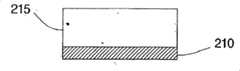
在图2A中,下电极或第一电极210是在基片(未示出)上构成的。第一电极210包含导电材料。实例包括导电掺杂的多晶硅、碳(C)、金属、合金、金属硅化物、导电金属氮化物和导电金属氧化物。第一电极210还可以包含一种以上的导电材料。例如,第一电极210可包含覆盖一层钼(Mo)层的碳层,或覆盖一层氮化钛(TiN)层的钨(W)层。此外,第一电极210可以包括一层或更多层毗连下衬层或覆盖层的粘附或屏障(barrier)层。任何粘附或屏障层优选应该是导电的,以便不干扰硫族化物存储元件200的编程。对于一种实施方案,第一电极210含有银。对于加一实施方案,第一电极210是一层银。In FIG. 2A, a lower or
第一电极210优选是利用物理汽相沉积(PVD)方法构成的。实施例包括本领域众所周知的真空或热蒸发、电子束蒸发和溅射方法。在PVD方法中,含待沉积材料的源或靶被蒸发,且可包括使部分或全部汽化的靶材料电离。然后,撞击在基片上的被汽化及/或电离的物种可沉积在该基片上。由于其形成高纯度层的总能力,PVD方法是优选的,仅受PVD方法所用物源或靶的纯度的限制。但是,也可采用其它沉积方法,诸如化学汽相沉积(CVD)方法,其中汽化了的化学前体被吸附在基片表面上,进行反应,构成第一电极210。The
对于一种实施方案,第一电极210厚度为约500-1000
在形成第一电极210后,在第一电极210上形成硫族化物层215。如与第一电极210那样,优选利用PVD方法形成硫族化物层215,但是也可利用其它沉积方法来形成。对于一种实施方案,硫族化物层215含一种硫族化物材料,其内含一种或更多种在传统IUPAC版周期表中的VIB族元素,即氧(O)、硫(S)、硒(Se)、碲(Te)及钋(Po),和一种或更多种在传统IUPAC版周期表中的IVB及VB族元素,即碳(C)、硅(Si)、锗(Ge)、锡(Sn)、铅(Pb)、氮(N)、磷(P)、砷(As)、锑(Sb)及铋(Bi)。更优选地是,硫族化物层215包含一种内含硒及/或碲与锗及/或锑组合的硫族化物材料。对于一种实施方案,硫族化物层215含一种硒化锗材料(GeSe或GeSe2)。After the
对于一种实施方案,硫族化物层215厚度为约300-700

如图2B所示,利用溅射方法对硫族化物层215掺杂金属240,形成一层掺杂后的硫族化物层230。此掺杂后的硫族化物层230被掺杂到所需掺杂水平。对于一种实施方案,此所需掺杂水平构成一层由金属240所饱和的掺杂后的硫族化物层230。对于另一实施方案,所需掺杂水平构成一层过饱和的掺杂后的硫族化物层230。对于再一实施方案,在掺杂后的硫族化物层230中,所需掺杂水平为约15-30重量%的金属240。As shown in FIG. 2B , the
用于进行溅射的设备的一个实例可包括ENDURA
图3为说明适用于本发明实施方案的一种PVD设备310的示意图。那些熟悉PVD设备的人们应承认,这是一种简化示意图,典型的PVD设备可以包含另外或替代的部件。Figure 3 is a schematic diagram illustrating a PVD apparatus 310 suitable for use in embodiments of the present invention. Those familiar with PVD equipment will recognize that this is a simplified schematic and that a typical PVD equipment may contain additional or alternative components.
包含基片312的导电基片314被放在沉积室316中。此基片314连接直流电源324。设置了一个把组分气体引至室316中的气体入口318。组分气体构成等离子322。在设备310操作过程中,一般不断地将这些组分气体加至沉积室316中。如这里所用,组分气体不包括在溅射过程中所产生的任何被汽化的靶材料。Conductive substrate 314 including substrate 312 is placed in deposition chamber 316 . The substrate 314 is connected to a DC power source 324 . A gas inlet 318 for introducing component gases into chamber 316 is provided. The component gases make up the plasma 322 . During operation of apparatus 310, these component gases are typically continuously fed into deposition chamber 316. As used herein, component gases do not include any vaporized target material produced during sputtering.
连接直流电源328的溅射靶326被安置在室316中。靶326可以是一块由待溅射材料构成的平板。在对硫族化物层215的掺杂中待溅射材料的实例包括高扩散金属,诸如铜、银、金及铝。用真空泵(未示出)经排气口329从沉积室316排放出过量或废气体。A sputtering target 326 connected to a DC power source 328 is positioned in the chamber 316 . Target 326 may be a flat plate of material to be sputtered. Examples of materials to be sputtered in doping the
在磁控管结构中,磁体327帮助形成等离子322。对作为阴极的靶326和作为阳极的基片312施加偏压,形成等离子322。磁体327通常置于靶326之后。In a magnetron configuration, magnets 327 assist in the formation of plasma 322 . The plasma 322 is formed by applying a bias voltage to the target 326 as the cathode and the substrate 312 as the anode. A magnet 327 is generally placed behind the target 326 .
为增加由等离子发射的UV成分,将低分子量的稀有气体添加至等离子中。尤其,用氖(Ne)及/或氦(He)至少部分地形成等离子。该等离子还可含其它组分气体。一个实例是氩(Ar),它在溅射工艺中是常常使用的。尽管氩的波谱也有UV成分,但与氖或氦相比,它的相对强度较低,因而造成金属扩散速率较低。对于一种实施方案,掺杂过程所用等离子是由基本上由氖构成的进料气体产生的。对于另一实施方案,掺杂过程所用等离子含有氦。对于再一实施方案,掺杂过程所用等离子至少含有氩和氖。由于其UV成分增加,等离子也可以由基本上由氦构成的进料气体产生,但是这种应用会导致溅射效率降低,而不理想。利用原子量较低的气体,可以产生比传统PVD方法高很多的操作压力,例如30-300毫乇。To increase the UV component emitted by the plasma, low molecular weight noble gases are added to the plasma. In particular, the plasma is at least partially formed with neon (Ne) and/or helium (He). The plasma may also contain other component gases. An example is argon (Ar), which is commonly used in sputtering processes. Although argon also has a UV component in its spectrum, its relative intensity is lower compared to neon or helium, resulting in a lower metal diffusion rate. For one embodiment, the plasma used in the doping process is generated from a feed gas consisting essentially of neon. For another embodiment, the plasma used in the doping process contains helium. For yet another embodiment, the plasma used in the doping process contains at least argon and neon. Plasma can also be generated from a feed gas consisting essentially of helium due to its increased UV content, but this application results in less efficient sputtering and is not ideal. Using lower atomic weight gases allows for much higher operating pressures than conventional PVD methods, eg 30-300 mTorr.
调节产生等离子所用气体的体积百分比,可产生其平均原子量为最低气体原子量和最高气体原子量之间任何值的等离子。以这种方式可以产生其平均原子量足以促进所需溅射效率的等离子。溅射效率一般指的是单位入射离子所喷出的靶原子的数量,典型范围在约0.5-1.5。溅射效率主要决定了溅射植入或沉积的速率。溅射效率取决于许多因素,包括入射离子方向、靶材料、轰击离子质量、轰击离子能量、剂量、晶体状态和表面结合能。Adjusting the volume percent of the gas used to generate the plasma produces a plasma having an average atomic weight anywhere between the lowest gas atomic weight and the highest gas atomic weight. In this way a plasma can be produced with an average atomic weight sufficient to promote the desired sputtering efficiency. Sputtering efficiency generally refers to the number of target atoms ejected per unit of incident ions, with a typical range of about 0.5-1.5. Sputtering efficiency primarily determines the rate of sputter implantation or deposition. Sputtering efficiency depends on many factors, including incident ion orientation, target material, bombarding ion mass, bombarding ion energy, dose, crystal state, and surface binding energy.
值得注意的是,在由两种以上的气体产生等离子时,这些气体的多重组合可以构成相同的平均原子量。例如,按体积计,由5%氩、78%氖和17%氦组成的混合物将大致具有与按体积计的10%氩、67%氖和23%氦组成的混合物相同的平均原子量。It is worth noting that when plasmas are generated from more than two gases, multiple combinations of these gases can constitute the same average atomic weight. For example, a mixture of 5% argon, 78% neon, and 17% helium by volume will have approximately the same average atomic weight as a mixture of 10% argon, 67% neon, and 23% helium by volume.
调节等离子中气体的体积百分比,也可产生一种等离子,其具有单个气体波谱复合的UV成分和具有一般在等离子中气体相对强度最低和气体相对强度最高之间的相对强度。以这种方式可以产生一种等离子,其复合UV成分的相对强度足以产生所需水平的光子诱发的被溅射金属扩散。应注意的是,由两种以上的气体产生等离子时,这些气体的多重组合可以发射具有相同相对强度的UV成分。Adjusting the volume percentage of the gas in the plasma also produces a plasma with a single gas spectrally complex UV component and with a relative intensity generally between the lowest relative intensity of the gas and the highest relative intensity of the gas in the plasma. In this way a plasma can be created whose recombined UV components are of sufficient relative strength to produce the desired level of photon-induced diffusion of the sputtered metal. It should be noted that when plasmas are generated from more than two gases, multiple combinations of these gases can emit UV components with the same relative intensity.
鉴于以上这些,通过选择两种或更多种的组分气体和其相对体积百分比,有可能选出使之具有其发射UV成分的所需相对强度和所需平均原子量的等离子。但是,应当承认,这些数值即所需相对强度和所需平均原子量可能是相互排斥的。换句话说,达到某一数值可能要求对另一数值做出让步。一种让步方法可能应是先确定产生具有所需相对强度的等离子的组分气体的组合,然后选择其中平均原子量接近于所需原子量的组分气体的组合中的一种。另一种方法是,先确定产生具有所需平均原子量的等离子的组分气体的组合,然后选择这些组合中一种其UV成分的相对强度接近于所需相对强度的组分气体的组合。In view of the above, by selecting two or more constituent gases and their relative volume percentages, it is possible to select a plasma having a desired relative intensity of its UV-emitting component and a desired average atomic weight. It should be recognized, however, that these values, the desired relative strength and the desired average atomic weight, may be mutually exclusive. In other words, reaching one value may require concessions to another. One compromise might be to first determine the combination of component gases that produce a plasma of the desired relative intensity, and then select one of the combinations of component gases in which the average atomic mass is close to the desired atomic mass. Alternatively, first determine combinations of component gases that produce a plasma of the desired average atomic weight, and then select one of these combinations that has a relative intensity of the UV component that is close to the desired relative intensity.
不同等离子的UV成分可能波谱不同,但相对强度却相同。因为波谱也会影响扩散速率,可能最好产生一种在所得等离子中特定的发射光谱。因此,对于一种实施方案,选择一种组分气体混合物以产生所得等离子的理想波谱。对于另一实施方案,选择一种组分气体混合物,以产生其所得等离子可见成分水平高于由氖构成的等离子的所需波谱。对于另一实施方案,选择一种能使所得等离子产生所需波谱的组分气体混合物,达到靶溅射效率。对于硫族化物层215进行掺杂,一般选择在溅射过程中所用的等离子的组分气体来产生所需的扩散和溅射速率。The UV components of different plasmas may have different spectra but the same relative intensity. Since the spectrum also affects the rate of diffusion, it may be desirable to produce a specific emission spectrum in the resulting plasma. Thus, for one embodiment, a component gas mixture is chosen to produce the desired spectrum of the resulting plasma. For another embodiment, a component gas mixture is selected to produce a desired spectrum with a higher level of visible constituents of the resulting plasma than a plasma composed of neon. For another embodiment, a target sputtering efficiency is achieved by selecting a component gas mixture that produces the desired spectrum of the resulting plasma. For doping of the
作为等离子组合物如何影响扩散的实例,利用不同的等离子,但其它方面类似的处理条件,进行了将银溅射至硒化锗上的试验。利用一种由基本上由氖构成的进料气体产生的等离子,溅射约501.6的银至约503


现返回参照图2C,上电极或第二电极250是在掺杂后的硫族化物层230上形成的。第二电极250一般采纳与第一电极210相同的准则。因此,第二电极250包含导电材料。实例包括导电掺杂的多晶硅、碳、金属(包括难熔金属)、合金、金属硅化物、导电金属氮化物和导电金属氧化物。第二电极250还可含一种以上的导电材料。此外,第二电极250可以包括一层或更多层的粘附或屏障层,毗连于下衬层或覆盖层。任何粘附或屏障层优选应该是导电的,以便不干扰硫族化物存储元件200的编程。对于一种实施方案,第二电极250含银。对于另一实施方案,第二电极250是一层银。Referring back now to FIG. 2C , an upper or
第二电极250优选是利用PVD方法形成的,但也可用其它如CVD方法形成。更优选地是,第二电极250是采用与对硫族化物层215进行掺杂过程中所用相同的PVD设备和靶来形成的。以这种方式,第二电极250可能是与掺杂过程一起原位形成的,因此进一步减少了与半导体基片输送有关的污染或损坏危险。因此,对于一种实施方案,第二电极250是通过溅射金属245至掺杂后的硫族化物层230上的方法形成的。The
对于一种实施方案,第二电极250厚度为约800-1200

对于一种实施方案,在第二电极250形成之前,排出沉积室316中对硫族化物层215进行掺杂所用的组分气体。对于这样的实施方案,对第二电极250的沉积,用新组分气体形成新等离子322。例如,可用基本上由氖构成的进料气体产生的等离子322,进行对硫族化物层215的掺杂。在达到所需掺杂水平之后,排空沉积室316。随后,可用基本上由氩构成的进料气体所产生的等离子322,形成第二电极。或者或另外,此第二等离子322可含氮或氧,以分别形成导电金属氮化物或金属氧化物。For one embodiment, the component gases used to dope the
或者,可以改变组分气体的进料组成,而不排空沉积室316。例如,可用一种组分气体和具有如基本上由氖构成的第一组成的等离子322,完成对硫族化物层215的掺杂。在接近所需掺杂水平时,可改变组分气体进料为第二组成,如基本上由氩构成。因此,对于此实施例,等离子322中的氩浓度将随对沉积室316添加氩和排出混合气体而逐渐增高。由于等离子322组成变化,倾向较高的平均原子量及/或较少的UV成分,动力学会远离扩散而转向沉积。为减少等离于322组成的变化率,可以逐渐改变组分气体的进料组成而步骤不变。Alternatively, the feed composition of the component gases may be changed without venting the deposition chamber 316 . For example, doping the
对于另一实施方案,可结合参照图2B和2C所述的处理,利用单一组成的等离子322。对于这一实施方案,选择组分气体要使扩散和沉积产生所需的组合。扩散速率相对于沉积速率应足够的高,以便在第二电极250厚度变得足以阻断金属进一步扩散进入该掺杂后硫族化物层230之前,充分进行掺杂。For another embodiment, a single composition plasma 322 may be utilized in conjunction with the processes described with reference to Figures 2B and 2C. For this embodiment, the component gases are chosen to result in the desired combination of diffusion and deposition. The rate of diffusion relative to the rate of deposition should be high enough to allow sufficient doping to occur before the
图2D显示第二电极250形成后的硫族化物存储元件200。该硫族化物存储元件200具有一层插在第一电极210和第二电极250之间的掺杂后的硫族化物层。该硫族化物存储元件200可用于形成硫族化物存储单元(cell),在此单元掺杂后的硫族化物层200的状态表示由存储单元写入的数据值。FIG. 2D shows the
图4表示按这里所述含硫族化物存储元件200的部分存储器阵列400的示意图。该存储器阵列400包括一般按行列排列的许多存储单元405。典型存储器阵列400包含数百万这些存储单元405。每个存储单元405包括一个耦联在第一导线(first conductive line)如字线410和二极管415之间的硫族化物存储元件200。二极管415又耦联在第二导线(second conductive line)如位线420和硫族化物存储元件200之间。或者,该二极管415可能耦联在第一导线和硫族化物存储元件200之间。该二极管415对存储单元300起存取器(access device)作用。被耦联至同一字线410的存储单元300的组合一般被称为一行存储单元。同样,被耦联至同一位线420的存储单元300的组合一般被称为一列存储单元。FIG. 4 shows a schematic diagram of a portion of a
图5为按照本发明实施方案的一种集成电路存储器件500的简化框图。存储器件500是一种内含按照本发明的硫族化物存储元件的非易失性存储器件。存储器件500包括含若干非易失性硫族化物存储元件的存储单元的阵列502。该存储阵列502是按多个可寻址存储库(addressable banks)排列。在一种实施方案中,该存储器含4个存储库504、506、508和510。各存储库含可寻址行和列的存储单元。Figure 5 is a simplified block diagram of an integrated circuit memory device 500 in accordance with an embodiment of the present invention. Memory device 500 is a nonvolatile memory device incorporating a chalcogenide memory element according to the present invention. Memory device 500 includes an array 502 of memory cells including a number of nonvolatile chalcogenide memory elements. The storage array 502 is arranged in addressable banks. In one embodiment, the memory contains four memory banks 504, 506, 508 and 510. Each memory bank contains addressable row and column memory cells.
可利用外部提供的由地址寄存器(address registers)512经地址信号接点(connections)528接受的位点地址,选取存储器阵列502中所写入的数据。利用存储库译码逻辑电路(bank decode logic)516,解码这些地址,选择目标存储库。也可利用行译码线路514,解码这些地址,选择目标行。还可利用列译码线路518,解码这些地址,以选择一个或更多个目标列。The data written in the memory array 502 can be selected by using the external address provided by the address registers (address registers) 512 and received by the address signal contacts (connections) 528 . These addresses are decoded using bank decode logic 516 to select the target bank. These addresses can also be decoded using the row decode circuit 514 to select the target row. These addresses can also be decoded using column decode circuitry 518 to select one or more target columns.
数据经数据连接点530通过I/O电路520而输入和输出。I/O电路528包括数据输出寄存器、输出驱动器和输出缓存器(output buffers)。指令执行逻辑电路522是提供来控制该存储器件500的基本操作,以响应于经控制信号连接点526所接受的控制信号。也可以提供一种状态机械装置(State machine)524,以控制在存储器阵列和单元上运行的具体操作。该指令执行逻辑电路522及/或状态机械装置524一般可被称为控制回路,用于控制读取、写入、删除及其它存储操作。数据连接点530一般用于双向数据信息交流。存储器可以被耦联至外处理机550上用于操作或进行检测。Data is input and output through I/O circuit 520 via data connection point 530 . The I/O circuit 528 includes data output registers, output drivers and output buffers. Instruction execution logic 522 is provided to control the basic operation of the memory device 500 in response to control signals received via control signal connection point 526 . A state machine (State machine) 524 may also be provided to control specific operations performed on the memory array and cells. The instruction execution logic 522 and/or the state machine 524 may generally be referred to as a control loop for controlling read, write, delete, and other storage operations. The data connection point 530 is generally used for two-way data communication. A memory may be coupled to the external processor 550 for operation or detection.
本领域技术人员应知道,可提供另外的电路和控制信号,且图5的存储器件已被简化,以有助于理解本发明。应当理解,以上对存储器件的说明是用于提供对存储器的一般认识,而非对典型存储器件所有元件和特征的完整叙述。Those skilled in the art will appreciate that additional circuitry and control signals may be provided, and that the memory device of FIG. 5 has been simplified to facilitate understanding of the present invention. It should be understood that the above description of the memory device is used to provide a general understanding of the memory, rather than a complete description of all elements and features of a typical memory device.
如本领域技术人员所公认的,这里所述类型的存储器件一般是按包含各种半导体器件的集成电路而制造的。集成电路由基片支撑。各基片上的集成电路一般被多次重复。如本领域众所用知,此基片还被进一步处理,以分离这些集成电路为电路小片(dies)。As will be recognized by those skilled in the art, memory devices of the type described herein are typically fabricated as integrated circuits comprising various semiconductor devices. Integrated circuits are supported by substrates. The integrated circuits on each substrate are typically repeated multiple times. The substrate is further processed to separate the integrated circuits into dies, as is known in the art.
以上各图是用于帮助理解所附文本的。但是,对这些图未按比例描绘,各单独部件和层的相对尺寸不一定表示这些部件或层各自应用中的相对尺寸。因此,附图不是用来表示量纲特征的。The figures above are provided to aid in the understanding of the accompanying text. However, the figures are not drawn to scale, and the relative sizes of individual components and layers do not necessarily indicate the relative sizes of these components or layers in their respective applications. Accordingly, the drawings are not intended to represent dimensional features.
尽管这里提供了量纲特征作为信息,但应承认,为缩小集成电路器件尺寸,增强性能和降低制造成本,仍然需继续努力。此外,这里所述概念基本不受绝对尺寸的限制。因此,期望在制造和传感技术方面做出有利于在此所述缩小硫族化物存储元件量纲特性的改进,尤其在它们涉及层厚方面。Although dimensional characteristics are provided here for information, it should be recognized that continuing efforts are needed to reduce integrated circuit device size, enhance performance, and reduce manufacturing costs. Furthermore, the concepts described herein are not substantially limited by absolute dimensions. Therefore, improvements in manufacturing and sensing technology are desired that facilitate the reduction of the dimensional properties of chalcogenide memory elements described here, especially as they relate to layer thicknesses.
结论in conclusion
现已描述了形成掺杂金属后的硫族化物层和含此掺杂后的硫族化物层器件的方法。这些方法包括利用等离子诱发金属扩散进入硫族化物层,同时发生金属沉积。该等离子含至少一种低原子量的稀有气体,如氖或氦。该等离子溅射率足以溅射金属靶,且其发射光谱的UV成分足以诱发该溅射金属扩散进入硫族化物层。利用这些方法,可在该掺杂后的硫族化物层上原位形成层导电层。在集成电路器件中,诸如在非易失性硫族化物的存储器件中,在金属沉积的同时对硫族化物层进行掺杂,和借助对硫族化物的掺杂使导电层的原位形成,减少对由于在刀具之间移动器件基片造成污染忧虑和物理损坏,从而促进器件可靠性的提高。Methods of forming metal doped chalcogenide layers and devices containing such doped chalcogenide layers have now been described. These methods involve the use of plasma-induced metal diffusion into the chalcogenide layer while metal deposition occurs. The plasma contains at least one noble gas of low atomic weight, such as neon or helium. The plasma sputtering rate is sufficient to sputter the metal target and the UV component of its emission spectrum is sufficient to induce diffusion of the sputtered metal into the chalcogenide layer. Using these methods, a layer conductive layer can be formed in situ on the doped chalcogenide layer. In integrated circuit devices, such as non-volatile chalcogenide memory devices, the chalcogenide layer is doped while the metal is deposited, and the in-situ formation of the conductive layer is achieved by doping the chalcogenide. , reducing contamination concerns and physical damage caused by moving the device substrate between tools, thereby promoting improved device reliability.
尽管这里已经说明和描述了若干具体实施方案,但本领域普通技术人员应当知道,为达到同一目标而计算的任何排列都可能替代所示具体实施方案。对本领域的普通技术人员而言,许多对本发明的修改都会是显而易见的。因此,本申请是要覆盖对本发明的任何修改或变异。显然要指出的是,本发明仅受以下各权利要求项和其等同项的限制。Although several specific embodiments have been illustrated and described herein, those of ordinary skill in the art will appreciate that any permutation calculated to achieve the same purpose may be substituted for the specific embodiment shown. Many modifications to the invention will be apparent to those of ordinary skill in the art. This application is therefore intended to cover any adaptations or variations of the present invention. It is expressly pointed out that the present invention is to be limited only by the terms of the following claims and their equivalents.
Claims (55)


Applications Claiming Priority (2)
| Application Number | Priority Date | Filing Date | Title |
|---|---|---|---|
| US09/943,426 | 2001-08-30 | ||
| US09/943,426US6709958B2 (en) | 2001-08-30 | 2001-08-30 | Integrated circuit device and fabrication using metal-doped chalcogenide materials |
Related Child Applications (1)
| Application Number | Title | Priority Date | Filing Date |
|---|---|---|---|
| CNB2007100854187ADivisionCN100550460C (en) | 2001-08-30 | 2002-08-30 | Utilize the integrated circuit (IC)-components and the manufacturing of the chalcogenide material behind the doping metals |
Publications (2)
| Publication Number | Publication Date |
|---|---|
| CN1578848A CN1578848A (en) | 2005-02-09 |
| CN100402694Ctrue CN100402694C (en) | 2008-07-16 |
Family
ID=25479641
Family Applications (2)
| Application Number | Title | Priority Date | Filing Date |
|---|---|---|---|
| CNB2007100854187AExpired - LifetimeCN100550460C (en) | 2001-08-30 | 2002-08-30 | Utilize the integrated circuit (IC)-components and the manufacturing of the chalcogenide material behind the doping metals |
| CNB028214501AExpired - LifetimeCN100402694C (en) | 2001-08-30 | 2002-08-30 | Integrated circuit devices and fabrication using metal-doped chalcogenide materials |
Family Applications Before (1)
| Application Number | Title | Priority Date | Filing Date |
|---|---|---|---|
| CNB2007100854187AExpired - LifetimeCN100550460C (en) | 2001-08-30 | 2002-08-30 | Utilize the integrated circuit (IC)-components and the manufacturing of the chalcogenide material behind the doping metals |
Country Status (8)
| Country | Link |
|---|---|
| US (4) | US6709958B2 (en) |
| EP (2) | EP1801898B1 (en) |
| JP (1) | JP4194490B2 (en) |
| KR (1) | KR100586716B1 (en) |
| CN (2) | CN100550460C (en) |
| AT (2) | ATE529540T1 (en) |
| DE (1) | DE60231129D1 (en) |
| WO (1) | WO2003020998A2 (en) |
Cited By (1)
| Publication number | Priority date | Publication date | Assignee | Title |
|---|---|---|---|---|
| CN106601911A (en)* | 2016-12-30 | 2017-04-26 | 中国科学院上海微系统与信息技术研究所 | Ge-Se-Al OTS material, OTS gate unit and preparation method thereof |
Families Citing this family (280)
| Publication number | Priority date | Publication date | Assignee | Title |
|---|---|---|---|---|
| US6542690B1 (en)* | 2000-05-08 | 2003-04-01 | Corning Incorporated | Chalcogenide doping of oxide glasses |
| JP4742429B2 (en)* | 2001-02-19 | 2011-08-10 | 住友電気工業株式会社 | Method for producing glass particulate deposit |
| US6734455B2 (en)* | 2001-03-15 | 2004-05-11 | Micron Technology, Inc. | Agglomeration elimination for metal sputter deposition of chalcogenides |
| DE10119463C2 (en)* | 2001-04-12 | 2003-03-06 | Hahn Meitner Inst Berlin Gmbh | Method for producing a chalcogenide semiconductor layer of type ABC¶2¶ with optical process control |
| US7102150B2 (en)* | 2001-05-11 | 2006-09-05 | Harshfield Steven T | PCRAM memory cell and method of making same |
| US6951805B2 (en)* | 2001-08-01 | 2005-10-04 | Micron Technology, Inc. | Method of forming integrated circuitry, method of forming memory circuitry, and method of forming random access memory circuitry |
| US6784018B2 (en)* | 2001-08-29 | 2004-08-31 | Micron Technology, Inc. | Method of forming chalcogenide comprising devices and method of forming a programmable memory cell of memory circuitry |
| US6881623B2 (en) | 2001-08-29 | 2005-04-19 | Micron Technology, Inc. | Method of forming chalcogenide comprising devices, method of forming a programmable memory cell of memory circuitry, and a chalcogenide comprising device |
| US6955940B2 (en)* | 2001-08-29 | 2005-10-18 | Micron Technology, Inc. | Method of forming chalcogenide comprising devices |
| US6709958B2 (en)* | 2001-08-30 | 2004-03-23 | Micron Technology, Inc. | Integrated circuit device and fabrication using metal-doped chalcogenide materials |
| US6646902B2 (en) | 2001-08-30 | 2003-11-11 | Micron Technology, Inc. | Method of retaining memory state in a programmable conductor RAM |
| US7109056B2 (en)* | 2001-09-20 | 2006-09-19 | Micron Technology, Inc. | Electro-and electroless plating of metal in the manufacture of PCRAM devices |
| US6612695B2 (en)* | 2001-11-07 | 2003-09-02 | Michael Waters | Lighted reading glasses |
| US6815818B2 (en)* | 2001-11-19 | 2004-11-09 | Micron Technology, Inc. | Electrode structure for use in an integrated circuit |
| US6791859B2 (en) | 2001-11-20 | 2004-09-14 | Micron Technology, Inc. | Complementary bit PCRAM sense amplifier and method of operation |
| US6909656B2 (en)* | 2002-01-04 | 2005-06-21 | Micron Technology, Inc. | PCRAM rewrite prevention |
| JP4218527B2 (en)* | 2002-02-01 | 2009-02-04 | 株式会社日立製作所 | Storage device |
| US6867064B2 (en)* | 2002-02-15 | 2005-03-15 | Micron Technology, Inc. | Method to alter chalcogenide glass for improved switching characteristics |
| US6791885B2 (en)* | 2002-02-19 | 2004-09-14 | Micron Technology, Inc. | Programmable conductor random access memory and method for sensing same |
| US7087919B2 (en)* | 2002-02-20 | 2006-08-08 | Micron Technology, Inc. | Layered resistance variable memory device and method of fabrication |
| US6847535B2 (en) | 2002-02-20 | 2005-01-25 | Micron Technology, Inc. | Removable programmable conductor memory card and associated read/write device and method of operation |
| US6809362B2 (en)* | 2002-02-20 | 2004-10-26 | Micron Technology, Inc. | Multiple data state memory cell |
| US7151273B2 (en)* | 2002-02-20 | 2006-12-19 | Micron Technology, Inc. | Silver-selenide/chalcogenide glass stack for resistance variable memory |
| US6937528B2 (en)* | 2002-03-05 | 2005-08-30 | Micron Technology, Inc. | Variable resistance memory and method for sensing same |
| US6849868B2 (en) | 2002-03-14 | 2005-02-01 | Micron Technology, Inc. | Methods and apparatus for resistance variable material cells |
| US6864500B2 (en)* | 2002-04-10 | 2005-03-08 | Micron Technology, Inc. | Programmable conductor memory cell structure |
| US6855975B2 (en)* | 2002-04-10 | 2005-02-15 | Micron Technology, Inc. | Thin film diode integrated with chalcogenide memory cell |
| US6858482B2 (en)* | 2002-04-10 | 2005-02-22 | Micron Technology, Inc. | Method of manufacture of programmable switching circuits and memory cells employing a glass layer |
| US20030205822A1 (en)* | 2002-05-02 | 2003-11-06 | Taiwan Semiconductor Manufacturing Co. Ltd. | Low-strength plasma treatment for interconnects |
| US6731528B2 (en)* | 2002-05-03 | 2004-05-04 | Micron Technology, Inc. | Dual write cycle programmable conductor memory system and method of operation |
| US6890790B2 (en)* | 2002-06-06 | 2005-05-10 | Micron Technology, Inc. | Co-sputter deposition of metal-doped chalcogenides |
| US6825135B2 (en)* | 2002-06-06 | 2004-11-30 | Micron Technology, Inc. | Elimination of dendrite formation during metal/chalcogenide glass deposition |
| US7209378B2 (en)* | 2002-08-08 | 2007-04-24 | Micron Technology, Inc. | Columnar 1T-N memory cell structure |
| US7018863B2 (en)* | 2002-08-22 | 2006-03-28 | Micron Technology, Inc. | Method of manufacture of a resistance variable memory cell |
| US6831019B1 (en)* | 2002-08-29 | 2004-12-14 | Micron Technology, Inc. | Plasma etching methods and methods of forming memory devices comprising a chalcogenide comprising layer received operably proximate conductive electrodes |
| US7294527B2 (en) | 2002-08-29 | 2007-11-13 | Micron Technology Inc. | Method of forming a memory cell |
| US7364644B2 (en)* | 2002-08-29 | 2008-04-29 | Micron Technology, Inc. | Silver selenide film stoichiometry and morphology control in sputter deposition |
| US6867114B2 (en)* | 2002-08-29 | 2005-03-15 | Micron Technology Inc. | Methods to form a memory cell with metal-rich metal chalcogenide |
| US6864521B2 (en)* | 2002-08-29 | 2005-03-08 | Micron Technology, Inc. | Method to control silver concentration in a resistance variable memory element |
| US7010644B2 (en)* | 2002-08-29 | 2006-03-07 | Micron Technology, Inc. | Software refreshed memory device and method |
| US7163837B2 (en) | 2002-08-29 | 2007-01-16 | Micron Technology, Inc. | Method of forming a resistance variable memory element |
| US7337160B2 (en)* | 2002-12-31 | 2008-02-26 | Bae Systems Information And Electronic Systems Integration Inc. | Use of radiation-hardened chalcogenide technology for spaceborne reconfigurable digital processing systems |
| US7531823B2 (en)* | 2003-01-23 | 2009-05-12 | Nec Corporation | Electron device, integrated electron device using same, and operating method using same |
| US7115927B2 (en) | 2003-02-24 | 2006-10-03 | Samsung Electronics Co., Ltd. | Phase changeable memory devices |
| US7402851B2 (en)* | 2003-02-24 | 2008-07-22 | Samsung Electronics Co., Ltd. | Phase changeable memory devices including nitrogen and/or silicon and methods for fabricating the same |
| US7022579B2 (en)* | 2003-03-14 | 2006-04-04 | Micron Technology, Inc. | Method for filling via with metal |
| US6930909B2 (en) | 2003-06-25 | 2005-08-16 | Micron Technology, Inc. | Memory device and methods of controlling resistance variation and resistance profile drift |
| US6961277B2 (en) | 2003-07-08 | 2005-11-01 | Micron Technology, Inc. | Method of refreshing a PCRAM memory device |
| US7061004B2 (en)* | 2003-07-21 | 2006-06-13 | Micron Technology, Inc. | Resistance variable memory elements and methods of formation |
| US6903361B2 (en) | 2003-09-17 | 2005-06-07 | Micron Technology, Inc. | Non-volatile memory structure |
| US7562375B2 (en)* | 2003-10-10 | 2009-07-14 | Microsoft Corporation | Fast channel change |
| US7583551B2 (en)* | 2004-03-10 | 2009-09-01 | Micron Technology, Inc. | Power management control and controlling memory refresh operations |
| US7098068B2 (en)* | 2004-03-10 | 2006-08-29 | Micron Technology, Inc. | Method of forming a chalcogenide material containing device |
| DE102004020297B4 (en)* | 2004-04-26 | 2007-06-21 | Infineon Technologies Ag | Process for producing resistively switching memory components |
| DE102004029436B4 (en)* | 2004-06-18 | 2009-03-05 | Qimonda Ag | A method of manufacturing a solid electrolyte material region |
| US20050287698A1 (en)* | 2004-06-28 | 2005-12-29 | Zhiyong Li | Use of chalcogen plasma to form chalcogenide switching materials for nanoscale electronic devices |
| US7354793B2 (en)* | 2004-08-12 | 2008-04-08 | Micron Technology, Inc. | Method of forming a PCRAM device incorporating a resistance-variable chalocogenide element |
| US7326950B2 (en)* | 2004-07-19 | 2008-02-05 | Micron Technology, Inc. | Memory device with switching glass layer |
| US7190048B2 (en)* | 2004-07-19 | 2007-03-13 | Micron Technology, Inc. | Resistance variable memory device and method of fabrication |
| US7365411B2 (en) | 2004-08-12 | 2008-04-29 | Micron Technology, Inc. | Resistance variable memory with temperature tolerant materials |
| US7151688B2 (en)* | 2004-09-01 | 2006-12-19 | Micron Technology, Inc. | Sensing of resistance variable memory devices |
| US7224598B2 (en)* | 2004-09-02 | 2007-05-29 | Hewlett-Packard Development Company, L.P. | Programming of programmable resistive memory devices |
| US20060102870A1 (en)* | 2004-10-20 | 2006-05-18 | Viens Jean F | Infrared detection material and method of production |
| US7106096B2 (en)* | 2004-11-11 | 2006-09-12 | International Business Machines Corporation | Circuit and method of controlling integrated circuit power consumption using phase change switches |
| US7608503B2 (en) | 2004-11-22 | 2009-10-27 | Macronix International Co., Ltd. | Side wall active pin memory and manufacturing method |
| US7138290B2 (en)* | 2004-12-03 | 2006-11-21 | Micron Technology, Inc. | Methods of depositing silver onto a metal selenide-comprising surface and methods of depositing silver onto a selenium-comprising surface |
| US7374174B2 (en)* | 2004-12-22 | 2008-05-20 | Micron Technology, Inc. | Small electrode for resistance variable devices |
| US20060131555A1 (en)* | 2004-12-22 | 2006-06-22 | Micron Technology, Inc. | Resistance variable devices with controllable channels |
| FR2880177B1 (en) | 2004-12-23 | 2007-05-18 | Commissariat Energie Atomique | MEMORY PMC HAVING IMPROVED RETENTION TIME AND WRITING SPEED |
| DE102005001253A1 (en)* | 2005-01-11 | 2006-07-20 | Infineon Technologies Ag | Memory cell arrangement for solid electrolyte memory cells has lower electrode and upper electrode and activated solid electrolyte material area between them as memory material area and whole of material area is coherently designed |
| US20060172067A1 (en)* | 2005-01-28 | 2006-08-03 | Energy Conversion Devices, Inc | Chemical vapor deposition of chalcogenide materials |
| DE102005005325B4 (en)* | 2005-02-04 | 2011-12-15 | Adesto Technology Corp., Inc. | Method for producing a resistively switching non-volatile memory cell |
| US7317200B2 (en) | 2005-02-23 | 2008-01-08 | Micron Technology, Inc. | SnSe-based limited reprogrammable cell |
| DE102005012047A1 (en)* | 2005-03-16 | 2006-09-28 | Infineon Technologies Ag | Solid-state electrolyte memory manufacture involves coating first electrode with solid-state electrolyte layer, and then forming second electrode on solid-state electrolyte layer |
| KR100694188B1 (en)* | 2005-03-22 | 2007-03-14 | 한국표준과학연구원 | Memory and its manufacturing method |
| US7269044B2 (en) | 2005-04-22 | 2007-09-11 | Micron Technology, Inc. | Method and apparatus for accessing a memory array |
| US7709289B2 (en) | 2005-04-22 | 2010-05-04 | Micron Technology, Inc. | Memory elements having patterned electrodes and method of forming the same |
| US7427770B2 (en) | 2005-04-22 | 2008-09-23 | Micron Technology, Inc. | Memory array for increased bit density |
| US7269079B2 (en) | 2005-05-16 | 2007-09-11 | Micron Technology, Inc. | Power circuits for reducing a number of power supply voltage taps required for sensing a resistive memory |
| US7696503B2 (en)* | 2005-06-17 | 2010-04-13 | Macronix International Co., Ltd. | Multi-level memory cell having phase change element and asymmetrical thermal boundary |
| US7238994B2 (en) | 2005-06-17 | 2007-07-03 | Macronix International Co., Ltd. | Thin film plate phase change ram circuit and manufacturing method |
| US20070007505A1 (en)* | 2005-07-07 | 2007-01-11 | Honeywell International Inc. | Chalcogenide PVD components |
| US7233520B2 (en)* | 2005-07-08 | 2007-06-19 | Micron Technology, Inc. | Process for erasing chalcogenide variable resistance memory bits |
| US20070007579A1 (en)* | 2005-07-11 | 2007-01-11 | Matrix Semiconductor, Inc. | Memory cell comprising a thin film three-terminal switching device having a metal source and /or drain region |
| US7274034B2 (en) | 2005-08-01 | 2007-09-25 | Micron Technology, Inc. | Resistance variable memory device with sputtered metal-chalcogenide region and method of fabrication |
| US7332735B2 (en)* | 2005-08-02 | 2008-02-19 | Micron Technology, Inc. | Phase change memory cell and method of formation |
| US7317567B2 (en)* | 2005-08-02 | 2008-01-08 | Micron Technology, Inc. | Method and apparatus for providing color changing thin film material |
| KR100682969B1 (en)* | 2005-08-04 | 2007-02-15 | 삼성전자주식회사 | Phase change material, phase change ram including the same and method of manufacturing and operating the same |
| US7579615B2 (en)* | 2005-08-09 | 2009-08-25 | Micron Technology, Inc. | Access transistor for memory device |
| US20070037316A1 (en)* | 2005-08-09 | 2007-02-15 | Micron Technology, Inc. | Memory cell contact using spacers |
| US7304368B2 (en)* | 2005-08-11 | 2007-12-04 | Micron Technology, Inc. | Chalcogenide-based electrokinetic memory element and method of forming the same |
| US7251154B2 (en) | 2005-08-15 | 2007-07-31 | Micron Technology, Inc. | Method and apparatus providing a cross-point memory array using a variable resistance memory cell and capacitance |
| KR100637235B1 (en)* | 2005-08-26 | 2006-10-20 | 삼성에스디아이 주식회사 | Plasma display panel |
| US7277313B2 (en)* | 2005-08-31 | 2007-10-02 | Micron Technology, Inc. | Resistance variable memory element with threshold device and method of forming the same |
| KR100694316B1 (en) | 2005-09-30 | 2007-03-14 | 한양대학교 산학협력단 | Method for manufacturing RERRAM device having excellent stability of oxide thin film using plasma gas treatment |
| US8969865B2 (en)* | 2005-10-12 | 2015-03-03 | Hewlett-Packard Development Company, L.P. | Semiconductor film composition |
| US20070080428A1 (en)* | 2005-10-12 | 2007-04-12 | Herman Gregory S | Semiconductor film composition |
| US7394088B2 (en) | 2005-11-15 | 2008-07-01 | Macronix International Co., Ltd. | Thermally contained/insulated phase change memory device and method (combined) |
| US7635855B2 (en) | 2005-11-15 | 2009-12-22 | Macronix International Co., Ltd. | I-shaped phase change memory cell |
| US7450411B2 (en)* | 2005-11-15 | 2008-11-11 | Macronix International Co., Ltd. | Phase change memory device and manufacturing method |
| US7786460B2 (en) | 2005-11-15 | 2010-08-31 | Macronix International Co., Ltd. | Phase change memory device and manufacturing method |
| US7414258B2 (en) | 2005-11-16 | 2008-08-19 | Macronix International Co., Ltd. | Spacer electrode small pin phase change memory RAM and manufacturing method |
| US7507986B2 (en)* | 2005-11-21 | 2009-03-24 | Macronix International Co., Ltd. | Thermal isolation for an active-sidewall phase change memory cell |
| US7479649B2 (en) | 2005-11-21 | 2009-01-20 | Macronix International Co., Ltd. | Vacuum jacketed electrode for phase change memory element |
| US7829876B2 (en)* | 2005-11-21 | 2010-11-09 | Macronix International Co., Ltd. | Vacuum cell thermal isolation for a phase change memory device |
| US7449710B2 (en) | 2005-11-21 | 2008-11-11 | Macronix International Co., Ltd. | Vacuum jacket for phase change memory element |
| CN100524878C (en) | 2005-11-21 | 2009-08-05 | 旺宏电子股份有限公司 | Programmable resistive material memory array with air-insulated cells |
| US7599217B2 (en)* | 2005-11-22 | 2009-10-06 | Macronix International Co., Ltd. | Memory cell device and manufacturing method |
| US7459717B2 (en) | 2005-11-28 | 2008-12-02 | Macronix International Co., Ltd. | Phase change memory cell and manufacturing method |
| US7688619B2 (en)* | 2005-11-28 | 2010-03-30 | Macronix International Co., Ltd. | Phase change memory cell and manufacturing method |
| US7521364B2 (en)* | 2005-12-02 | 2009-04-21 | Macronix Internation Co., Ltd. | Surface topology improvement method for plug surface areas |
| FR2895531B1 (en)* | 2005-12-23 | 2008-05-09 | Commissariat Energie Atomique | IMPROVED METHOD FOR MAKING MEMORY CELLS OF THE PMC TYPE |
| US7531825B2 (en) | 2005-12-27 | 2009-05-12 | Macronix International Co., Ltd. | Method for forming self-aligned thermal isolation cell for a variable resistance memory array |
| US8062833B2 (en) | 2005-12-30 | 2011-11-22 | Macronix International Co., Ltd. | Chalcogenide layer etching method |
| US7595218B2 (en) | 2006-01-09 | 2009-09-29 | Macronix International Co., Ltd. | Programmable resistive RAM and manufacturing method |
| US7560337B2 (en) | 2006-01-09 | 2009-07-14 | Macronix International Co., Ltd. | Programmable resistive RAM and manufacturing method |
| US7741636B2 (en) | 2006-01-09 | 2010-06-22 | Macronix International Co., Ltd. | Programmable resistive RAM and manufacturing method |
| US7432206B2 (en) | 2006-01-24 | 2008-10-07 | Macronix International Co., Ltd. | Self-aligned manufacturing method, and manufacturing method for thin film fuse phase change ram |
| US7956358B2 (en) | 2006-02-07 | 2011-06-07 | Macronix International Co., Ltd. | I-shaped phase change memory cell with thermal isolation |
| DE102006009254B3 (en)* | 2006-02-28 | 2007-07-12 | Infineon Technologies Ag | Method for producing an integrated electronic circuit with programmable resistive cells, corresponding cells and data memories with such |
| US8492810B2 (en)* | 2006-02-28 | 2013-07-23 | Qimonda Ag | Method of fabricating an integrated electronic circuit with programmable resistance cells |
| US8936702B2 (en)* | 2006-03-07 | 2015-01-20 | Micron Technology, Inc. | System and method for sputtering a tensile silicon nitride film |
| US7554144B2 (en) | 2006-04-17 | 2009-06-30 | Macronix International Co., Ltd. | Memory device and manufacturing method |
| US7928421B2 (en)* | 2006-04-21 | 2011-04-19 | Macronix International Co., Ltd. | Phase change memory cell with vacuum spacer |
| KR100782482B1 (en)* | 2006-05-19 | 2007-12-05 | 삼성전자주식회사 | A phase change memory cell employing a thin film as a phase change material film, a phase change memory device having the same, an electronic device having the same, and a manufacturing method thereof |
| US7423300B2 (en)* | 2006-05-24 | 2008-09-09 | Macronix International Co., Ltd. | Single-mask phase change memory element |
| JP5145217B2 (en)* | 2006-05-31 | 2013-02-13 | ルネサスエレクトロニクス株式会社 | Semiconductor device |
| US7825033B2 (en)* | 2006-06-09 | 2010-11-02 | Micron Technology, Inc. | Methods of forming variable resistance memory cells, and methods of etching germanium, antimony, and tellurium-comprising materials |
| TWI303875B (en)* | 2006-06-16 | 2008-12-01 | Ind Tech Res Inst | Confined spacer phase change memory and fabrication method thereof |
| US7696506B2 (en)* | 2006-06-27 | 2010-04-13 | Macronix International Co., Ltd. | Memory cell with memory material insulation and manufacturing method |
| KR100631400B1 (en)* | 2006-06-29 | 2006-10-04 | 주식회사 아이피에스 | Chalcogenide Film Deposition Method for Phase Change Memory |
| KR100791071B1 (en)* | 2006-07-04 | 2008-01-02 | 삼성전자주식회사 | Programmable device once, electronic system having same and method of operation thereof |
| US7785920B2 (en) | 2006-07-12 | 2010-08-31 | Macronix International Co., Ltd. | Method for making a pillar-type phase change memory element |
| CN100452319C (en)* | 2006-07-14 | 2009-01-14 | 上海华虹Nec电子有限公司 | Making method for silicide damaged by low plasma inducing growth |
| US8115282B2 (en)* | 2006-07-25 | 2012-02-14 | Adesto Technology Corporation | Memory cell device and method of manufacture |
| KR100838527B1 (en) | 2006-07-31 | 2008-06-17 | 삼성전자주식회사 | Phase change memory device formation method |
| US7560723B2 (en)* | 2006-08-29 | 2009-07-14 | Micron Technology, Inc. | Enhanced memory density resistance variable memory cells, arrays, devices and systems including the same, and methods of fabrication |
| US7772581B2 (en) | 2006-09-11 | 2010-08-10 | Macronix International Co., Ltd. | Memory device having wide area phase change element and small electrode contact area |
| KR100829601B1 (en)* | 2006-09-27 | 2008-05-14 | 삼성전자주식회사 | Chalcogen compound target, manufacturing method thereof and manufacturing method of phase change memory device |
| US7504653B2 (en) | 2006-10-04 | 2009-03-17 | Macronix International Co., Ltd. | Memory cell device with circumferentially-extending memory element |
| US7510929B2 (en) | 2006-10-18 | 2009-03-31 | Macronix International Co., Ltd. | Method for making memory cell device |
| US7863655B2 (en) | 2006-10-24 | 2011-01-04 | Macronix International Co., Ltd. | Phase change memory cells with dual access devices |
| US7682868B2 (en)* | 2006-12-06 | 2010-03-23 | Macronix International Co., Ltd. | Method for making a keyhole opening during the manufacture of a memory cell |
| US7473576B2 (en) | 2006-12-06 | 2009-01-06 | Macronix International Co., Ltd. | Method for making a self-converged void and bottom electrode for memory cell |
| US7476587B2 (en) | 2006-12-06 | 2009-01-13 | Macronix International Co., Ltd. | Method for making a self-converged memory material element for memory cell |
| US7903447B2 (en) | 2006-12-13 | 2011-03-08 | Macronix International Co., Ltd. | Method, apparatus and computer program product for read before programming process on programmable resistive memory cell |
| US8344347B2 (en) | 2006-12-15 | 2013-01-01 | Macronix International Co., Ltd. | Multi-layer electrode structure |
| US7718989B2 (en)* | 2006-12-28 | 2010-05-18 | Macronix International Co., Ltd. | Resistor random access memory cell device |
| US7433226B2 (en)* | 2007-01-09 | 2008-10-07 | Macronix International Co., Ltd. | Method, apparatus and computer program product for read before programming process on multiple programmable resistive memory cell |
| US7440315B2 (en)* | 2007-01-09 | 2008-10-21 | Macronix International Co., Ltd. | Method, apparatus and computer program product for stepped reset programming process on programmable resistive memory cell |
| US7535756B2 (en) | 2007-01-31 | 2009-05-19 | Macronix International Co., Ltd. | Method to tighten set distribution for PCRAM |
| US7663135B2 (en) | 2007-01-31 | 2010-02-16 | Macronix International Co., Ltd. | Memory cell having a side electrode contact |
| US7701759B2 (en) | 2007-02-05 | 2010-04-20 | Macronix International Co., Ltd. | Memory cell device and programming methods |
| US7483292B2 (en) | 2007-02-07 | 2009-01-27 | Macronix International Co., Ltd. | Memory cell with separate read and program paths |
| US7463512B2 (en) | 2007-02-08 | 2008-12-09 | Macronix International Co., Ltd. | Memory element with reduced-current phase change element |
| US8138028B2 (en) | 2007-02-12 | 2012-03-20 | Macronix International Co., Ltd | Method for manufacturing a phase change memory device with pillar bottom electrode |
| US7884343B2 (en) | 2007-02-14 | 2011-02-08 | Macronix International Co., Ltd. | Phase change memory cell with filled sidewall memory element and method for fabricating the same |
| KR100888145B1 (en)* | 2007-02-22 | 2009-03-13 | 성균관대학교산학협력단 | Stress-free flexible circuit board manufacturing apparatus and method |
| US7956344B2 (en) | 2007-02-27 | 2011-06-07 | Macronix International Co., Ltd. | Memory cell with memory element contacting ring-shaped upper end of bottom electrode |
| US8268664B2 (en)* | 2007-03-05 | 2012-09-18 | Altis Semiconductor | Methods of manufacturing a semiconductor device; method of manufacturing a memory cell; semiconductor device; semiconductor processing device; integrated circuit having a memory cell |
| US7786461B2 (en) | 2007-04-03 | 2010-08-31 | Macronix International Co., Ltd. | Memory structure with reduced-size memory element between memory material portions |
| US8610098B2 (en)* | 2007-04-06 | 2013-12-17 | Macronix International Co., Ltd. | Phase change memory bridge cell with diode isolation device |
| US7755076B2 (en)* | 2007-04-17 | 2010-07-13 | Macronix International Co., Ltd. | 4F2 self align side wall active phase change memory |
| US7569844B2 (en) | 2007-04-17 | 2009-08-04 | Macronix International Co., Ltd. | Memory cell sidewall contacting side electrode |
| US7483316B2 (en)* | 2007-04-24 | 2009-01-27 | Macronix International Co., Ltd. | Method and apparatus for refreshing programmable resistive memory |
| US8846516B2 (en)* | 2007-07-06 | 2014-09-30 | Micron Technology, Inc. | Dielectric charge-trapping materials having doped metal sites |
| US8513637B2 (en)* | 2007-07-13 | 2013-08-20 | Macronix International Co., Ltd. | 4F2 self align fin bottom electrodes FET drive phase change memory |
| US7884342B2 (en) | 2007-07-31 | 2011-02-08 | Macronix International Co., Ltd. | Phase change memory bridge cell |
| US7729161B2 (en) | 2007-08-02 | 2010-06-01 | Macronix International Co., Ltd. | Phase change memory with dual word lines and source lines and method of operating same |
| US9018615B2 (en)* | 2007-08-03 | 2015-04-28 | Macronix International Co., Ltd. | Resistor random access memory structure having a defined small area of electrical contact |
| JP5088036B2 (en) | 2007-08-06 | 2012-12-05 | ソニー株式会社 | Storage element and storage device |
| US7642125B2 (en) | 2007-09-14 | 2010-01-05 | Macronix International Co., Ltd. | Phase change memory cell in via array with self-aligned, self-converged bottom electrode and method for manufacturing |
| US8178386B2 (en) | 2007-09-14 | 2012-05-15 | Macronix International Co., Ltd. | Phase change memory cell array with self-converged bottom electrode and method for manufacturing |
| US7551473B2 (en) | 2007-10-12 | 2009-06-23 | Macronix International Co., Ltd. | Programmable resistive memory with diode structure |
| FR2922368A1 (en) | 2007-10-16 | 2009-04-17 | Commissariat Energie Atomique | METHOD FOR MANUFACTURING A CBRAM MEMORY HAVING IMPROVED RELIABILITY |
| US7919766B2 (en) | 2007-10-22 | 2011-04-05 | Macronix International Co., Ltd. | Method for making self aligning pillar memory cell device |
| US7804083B2 (en) | 2007-11-14 | 2010-09-28 | Macronix International Co., Ltd. | Phase change memory cell including a thermal protect bottom electrode and manufacturing methods |
| US8039926B2 (en)* | 2007-12-06 | 2011-10-18 | Electronics And Telecommunications Research Institute | Method for manufacturing N-type and P-type chalcogenide material, doped homojunction chalcogenide thin film transistor and method of fabricating the same |
| US7646631B2 (en) | 2007-12-07 | 2010-01-12 | Macronix International Co., Ltd. | Phase change memory cell having interface structures with essentially equal thermal impedances and manufacturing methods |
| KR20090076077A (en)* | 2008-01-07 | 2009-07-13 | 삼성전자주식회사 | Resistive memory devices |
| US7639527B2 (en) | 2008-01-07 | 2009-12-29 | Macronix International Co., Ltd. | Phase change memory dynamic resistance test and manufacturing methods |
| US7879643B2 (en) | 2008-01-18 | 2011-02-01 | Macronix International Co., Ltd. | Memory cell with memory element contacting an inverted T-shaped bottom electrode |
| US7879645B2 (en) | 2008-01-28 | 2011-02-01 | Macronix International Co., Ltd. | Fill-in etching free pore device |
| KR101480292B1 (en)* | 2008-03-17 | 2015-01-12 | 삼성전자주식회사 | Methods of forming a semiconductor device including a phase change layer |
| US8084842B2 (en) | 2008-03-25 | 2011-12-27 | Macronix International Co., Ltd. | Thermally stabilized electrode structure |
| US8030634B2 (en) | 2008-03-31 | 2011-10-04 | Macronix International Co., Ltd. | Memory array with diode driver and method for fabricating the same |
| FR2929759B1 (en)* | 2008-04-03 | 2010-04-16 | Commissariat Energie Atomique | MAGNETIC DEVICE INCORPORATING A MAGNETORESISTIVE STACK |
| US7825398B2 (en) | 2008-04-07 | 2010-11-02 | Macronix International Co., Ltd. | Memory cell having improved mechanical stability |
| US7791057B2 (en) | 2008-04-22 | 2010-09-07 | Macronix International Co., Ltd. | Memory cell having a buried phase change region and method for fabricating the same |
| US8077505B2 (en) | 2008-05-07 | 2011-12-13 | Macronix International Co., Ltd. | Bipolar switching of phase change device |
| US7701750B2 (en) | 2008-05-08 | 2010-04-20 | Macronix International Co., Ltd. | Phase change device having two or more substantial amorphous regions in high resistance state |
| KR100974069B1 (en)* | 2008-06-02 | 2010-08-04 | 한국과학기술원 | Resistance change memory and manufacturing method |
| US8415651B2 (en) | 2008-06-12 | 2013-04-09 | Macronix International Co., Ltd. | Phase change memory cell having top and bottom sidewall contacts |
| US8134857B2 (en) | 2008-06-27 | 2012-03-13 | Macronix International Co., Ltd. | Methods for high speed reading operation of phase change memory and device employing same |
| US7932506B2 (en) | 2008-07-22 | 2011-04-26 | Macronix International Co., Ltd. | Fully self-aligned pore-type memory cell having diode access device |
| US8467236B2 (en)* | 2008-08-01 | 2013-06-18 | Boise State University | Continuously variable resistor |
| US7825479B2 (en) | 2008-08-06 | 2010-11-02 | International Business Machines Corporation | Electrical antifuse having a multi-thickness dielectric layer |
| US7903457B2 (en) | 2008-08-19 | 2011-03-08 | Macronix International Co., Ltd. | Multiple phase change materials in an integrated circuit for system on a chip application |
| US7719913B2 (en) | 2008-09-12 | 2010-05-18 | Macronix International Co., Ltd. | Sensing circuit for PCRAM applications |
| US8324605B2 (en) | 2008-10-02 | 2012-12-04 | Macronix International Co., Ltd. | Dielectric mesh isolated phase change structure for phase change memory |
| US7897954B2 (en)* | 2008-10-10 | 2011-03-01 | Macronix International Co., Ltd. | Dielectric-sandwiched pillar memory device |
| US8036014B2 (en)* | 2008-11-06 | 2011-10-11 | Macronix International Co., Ltd. | Phase change memory program method without over-reset |
| US7869270B2 (en) | 2008-12-29 | 2011-01-11 | Macronix International Co., Ltd. | Set algorithm for phase change memory cell |
| US8148707B2 (en)* | 2008-12-30 | 2012-04-03 | Stmicroelectronics S.R.L. | Ovonic threshold switch film composition for TSLAGS material |
| US8089137B2 (en) | 2009-01-07 | 2012-01-03 | Macronix International Co., Ltd. | Integrated circuit memory with single crystal silicon on silicide driver and manufacturing method |
| US8107283B2 (en) | 2009-01-12 | 2012-01-31 | Macronix International Co., Ltd. | Method for setting PCRAM devices |
| US8030635B2 (en) | 2009-01-13 | 2011-10-04 | Macronix International Co., Ltd. | Polysilicon plug bipolar transistor for phase change memory |
| US8064247B2 (en) | 2009-01-14 | 2011-11-22 | Macronix International Co., Ltd. | Rewritable memory device based on segregation/re-absorption |
| US8933536B2 (en) | 2009-01-22 | 2015-01-13 | Macronix International Co., Ltd. | Polysilicon pillar bipolar transistor with self-aligned memory element |
| US8084760B2 (en) | 2009-04-20 | 2011-12-27 | Macronix International Co., Ltd. | Ring-shaped electrode and manufacturing method for same |
| CN101525738B (en)* | 2009-04-23 | 2011-05-11 | 哈尔滨工业大学 | Internal surface ion implantation modification device and method of inductively coupled plasmatube barrel |
| US8173987B2 (en) | 2009-04-27 | 2012-05-08 | Macronix International Co., Ltd. | Integrated circuit 3D phase change memory array and manufacturing method |
| US8097871B2 (en) | 2009-04-30 | 2012-01-17 | Macronix International Co., Ltd. | Low operational current phase change memory structures |
| US7933139B2 (en) | 2009-05-15 | 2011-04-26 | Macronix International Co., Ltd. | One-transistor, one-resistor, one-capacitor phase change memory |
| US8350316B2 (en) | 2009-05-22 | 2013-01-08 | Macronix International Co., Ltd. | Phase change memory cells having vertical channel access transistor and memory plane |
| US7968876B2 (en) | 2009-05-22 | 2011-06-28 | Macronix International Co., Ltd. | Phase change memory cell having vertical channel access transistor |
| US8168538B2 (en)* | 2009-05-26 | 2012-05-01 | Macronix International Co., Ltd. | Buried silicide structure and method for making |
| WO2010140210A1 (en)* | 2009-06-01 | 2010-12-09 | 株式会社日立製作所 | Semiconductor memory device and manufacturing method thereof |
| US8809829B2 (en) | 2009-06-15 | 2014-08-19 | Macronix International Co., Ltd. | Phase change memory having stabilized microstructure and manufacturing method |
| US8406033B2 (en) | 2009-06-22 | 2013-03-26 | Macronix International Co., Ltd. | Memory device and method for sensing and fixing margin cells |
| US8238149B2 (en) | 2009-06-25 | 2012-08-07 | Macronix International Co., Ltd. | Methods and apparatus for reducing defect bits in phase change memory |
| US8363463B2 (en) | 2009-06-25 | 2013-01-29 | Macronix International Co., Ltd. | Phase change memory having one or more non-constant doping profiles |
| US8110822B2 (en) | 2009-07-15 | 2012-02-07 | Macronix International Co., Ltd. | Thermal protect PCRAM structure and methods for making |
| US8198619B2 (en) | 2009-07-15 | 2012-06-12 | Macronix International Co., Ltd. | Phase change memory cell structure |
| US7894254B2 (en) | 2009-07-15 | 2011-02-22 | Macronix International Co., Ltd. | Refresh circuitry for phase change memory |
| US8064248B2 (en) | 2009-09-17 | 2011-11-22 | Macronix International Co., Ltd. | 2T2R-1T1R mix mode phase change memory array |
| KR101243837B1 (en) | 2009-10-23 | 2013-03-20 | 한국전자통신연구원 | structure connecting multi-layer line and manufacturing method at the same |
| US8178387B2 (en) | 2009-10-23 | 2012-05-15 | Macronix International Co., Ltd. | Methods for reducing recrystallization time for a phase change material |
| US8198124B2 (en) | 2010-01-05 | 2012-06-12 | Micron Technology, Inc. | Methods of self-aligned growth of chalcogenide memory access device |
| US8729521B2 (en) | 2010-05-12 | 2014-05-20 | Macronix International Co., Ltd. | Self aligned fin-type programmable memory cell |
| FR2960884B1 (en)* | 2010-06-02 | 2012-06-01 | Commissariat Energie Atomique | METHOD FOR DIFFUSING METALLIC PARTICLES WITHIN A COMPOSITE LAYER |
| FR2961018B1 (en)* | 2010-06-04 | 2012-07-20 | Altis Semiconductor Snc | METHOD FOR MANUFACTURING A PROGRAMMABLE MEMORY MICROELECTRONIC DEVICE |
| US8310864B2 (en) | 2010-06-15 | 2012-11-13 | Macronix International Co., Ltd. | Self-aligned bit line under word line memory array |
| US8395935B2 (en) | 2010-10-06 | 2013-03-12 | Macronix International Co., Ltd. | Cross-point self-aligned reduced cell size phase change memory |
| JP5348108B2 (en)* | 2010-10-18 | 2013-11-20 | ソニー株式会社 | Memory element |
| US8497705B2 (en) | 2010-11-09 | 2013-07-30 | Macronix International Co., Ltd. | Phase change device for interconnection of programmable logic device |
| US8467238B2 (en) | 2010-11-15 | 2013-06-18 | Macronix International Co., Ltd. | Dynamic pulse operation for phase change memory |
| US8426242B2 (en)* | 2011-02-01 | 2013-04-23 | Macronix International Co., Ltd. | Composite target sputtering for forming doped phase change materials |
| US8497182B2 (en) | 2011-04-19 | 2013-07-30 | Macronix International Co., Ltd. | Sidewall thin film electrode with self-aligned top electrode and programmable resistance memory |
| US8605495B2 (en) | 2011-05-09 | 2013-12-10 | Macronix International Co., Ltd. | Isolation device free memory |
| US8946666B2 (en) | 2011-06-23 | 2015-02-03 | Macronix International Co., Ltd. | Ge-Rich GST-212 phase change memory materials |
| US8525290B2 (en) | 2011-06-24 | 2013-09-03 | Macronix International Co., Ltd. | Method of forming memory cell access device |
| US20130017647A1 (en)* | 2011-07-13 | 2013-01-17 | Applied Nanotech Holdings, Inc. | Surface-modified nanoparticle ink for photovoltaic applications |
| US9054295B2 (en) | 2011-08-23 | 2015-06-09 | Micron Technology, Inc. | Phase change memory cells including nitrogenated carbon materials, methods of forming the same, and phase change memory devices including nitrogenated carbon materials |
| US8916414B2 (en) | 2013-03-13 | 2014-12-23 | Macronix International Co., Ltd. | Method for making memory cell by melting phase change material in confined space |
| KR101500944B1 (en)* | 2013-03-22 | 2015-03-10 | 경희대학교 산학협력단 | Method for growing 2d layer of chacogenide compound, method for preparing cmos type structure, layer of chacogenide compound, electronic device including layer of chacogenide compound and cmos type structure |
| US9171616B2 (en) | 2013-08-09 | 2015-10-27 | Macronix International Co., Ltd. | Memory with multiple levels of data retention |
| US9478419B2 (en) | 2013-12-18 | 2016-10-25 | Asm Ip Holding B.V. | Sulfur-containing thin films |
| US9245742B2 (en) | 2013-12-18 | 2016-01-26 | Asm Ip Holding B.V. | Sulfur-containing thin films |
| US9336879B2 (en) | 2014-01-24 | 2016-05-10 | Macronix International Co., Ltd. | Multiple phase change materials in an integrated circuit for system on a chip application |
| KR101465211B1 (en)* | 2014-02-17 | 2014-11-25 | 성균관대학교산학협력단 | Preparing method of doped metal-chalcogenide thin film |
| US9559113B2 (en) | 2014-05-01 | 2017-01-31 | Macronix International Co., Ltd. | SSL/GSL gate oxide in 3D vertical channel NAND |
| US9159412B1 (en) | 2014-07-15 | 2015-10-13 | Macronix International Co., Ltd. | Staggered write and verify for phase change memory |
| US9118006B1 (en)* | 2014-08-12 | 2015-08-25 | Boise State University | Carbon-chalcogenide variable resistance memory device |
| DE102014119088A1 (en)* | 2014-12-18 | 2016-06-23 | Infineon Technologies Ag | A method of forming a semiconductor device and a semiconductor substrate |
| US9461134B1 (en) | 2015-05-20 | 2016-10-04 | Asm Ip Holding B.V. | Method for forming source/drain contact structure with chalcogen passivation |
| US10490475B2 (en) | 2015-06-03 | 2019-11-26 | Asm Ip Holding B.V. | Methods for semiconductor passivation by nitridation after oxide removal |
| US9711350B2 (en) | 2015-06-03 | 2017-07-18 | Asm Ip Holding B.V. | Methods for semiconductor passivation by nitridation |
| US9741815B2 (en) | 2015-06-16 | 2017-08-22 | Asm Ip Holding B.V. | Metal selenide and metal telluride thin films for semiconductor device applications |
| US9711396B2 (en) | 2015-06-16 | 2017-07-18 | Asm Ip Holding B.V. | Method for forming metal chalcogenide thin films on a semiconductor device |
| US9672906B2 (en) | 2015-06-19 | 2017-06-06 | Macronix International Co., Ltd. | Phase change memory with inter-granular switching |
| US9917252B2 (en) | 2015-06-19 | 2018-03-13 | Macronix International Co., Ltd. | GaSbGe phase change memory materials |
| US9472274B1 (en) | 2015-07-01 | 2016-10-18 | Macronix International Co., Ltd. | Refresh of nonvolatile memory cells and reference cells with resistance drift |
| KR101962336B1 (en)* | 2016-12-26 | 2019-07-18 | 전북대학교 산학협력단 | Coating layer using sacrificial metal oxide layer, manufacturing method thereof and sputtring wheel using the same |
| US10008665B1 (en)* | 2016-12-27 | 2018-06-26 | Intel Corporation | Doping of selector and storage materials of a memory cell |
| TWI627301B (en)* | 2017-02-17 | 2018-06-21 | 國立清華大學 | Method for preparing vertical heterojunction of metal chalcogenide |
| US10050196B1 (en) | 2017-05-04 | 2018-08-14 | Macronix International Co., Ltd. | Dielectric doped, Sb-rich GST phase change memory |
| US10541271B2 (en) | 2017-10-18 | 2020-01-21 | Macronix International Co., Ltd. | Superlattice-like switching devices |
| US10374009B1 (en) | 2018-07-17 | 2019-08-06 | Macronix International Co., Ltd. | Te-free AsSeGe chalcogenides for selector devices and memory devices using same |
| KR102636534B1 (en)* | 2018-08-20 | 2024-02-15 | 에스케이하이닉스 주식회사 | Chalcogenide material and electronic device including the same |
| KR102752636B1 (en) | 2019-09-17 | 2025-01-10 | 에스케이하이닉스 주식회사 | Chalcogenide material, variable resistive memory and electronic device |
| US11289540B2 (en) | 2019-10-15 | 2022-03-29 | Macronix International Co., Ltd. | Semiconductor device and memory cell |
| US20220406998A1 (en)* | 2019-11-22 | 2022-12-22 | Agency For Science, Technology And Research | Electronic synapse device and method of forming the same |
| US11515147B2 (en) | 2019-12-09 | 2022-11-29 | Micron Technology, Inc. | Material deposition systems, and related methods |
| US11158787B2 (en) | 2019-12-17 | 2021-10-26 | Macronix International Co., Ltd. | C—As—Se—Ge ovonic materials for selector devices and memory devices using same |
| US11362276B2 (en) | 2020-03-27 | 2022-06-14 | Macronix International Co., Ltd. | High thermal stability SiOx doped GeSbTe materials suitable for embedded PCM application |
| KR102509798B1 (en)* | 2021-04-20 | 2023-03-14 | 고려대학교 산학협력단 | Method for doping of transition metal dichalcogenide |
| CN114744109A (en)* | 2022-03-30 | 2022-07-12 | 华中科技大学 | Tetrahedral structure compound doped Sb-Te phase change material, phase change memory |
| US12310031B2 (en) | 2022-07-08 | 2025-05-20 | Macronix International Co., Ltd. | Multi-layer ovonic threshold switch (OTS) for switching devices and memory devices using the same |
| CN120302812A (en)* | 2025-06-12 | 2025-07-11 | 晶科能源(海宁)有限公司 | Laminated battery and method for making the same |
Citations (2)
| Publication number | Priority date | Publication date | Assignee | Title |
|---|---|---|---|---|
| US4089714A (en)* | 1977-01-06 | 1978-05-16 | Honeywell Inc. | Doping mercury cadmium telluride with aluminum or silicon |
| US5667645A (en)* | 1996-06-28 | 1997-09-16 | Micron Technology, Inc. | Method of sputter deposition |
Family Cites Families (170)
| Publication number | Priority date | Publication date | Assignee | Title |
|---|---|---|---|---|
| US72188A (en)* | 1867-12-17 | Elliott p | ||
| DE202896C (en)* | ||||
| DE1419289A1 (en) | 1961-01-26 | 1968-12-12 | Siemens Ag | Process for producing doped semiconductor bodies |
| US3622319A (en) | 1966-10-20 | 1971-11-23 | Western Electric Co | Nonreflecting photomasks and methods of making same |
| LU52765A1 (en) | 1967-01-06 | 1968-08-06 | ||
| US3743847A (en) | 1971-06-01 | 1973-07-03 | Motorola Inc | Amorphous silicon film as a uv filter |
| US4267261A (en)* | 1971-07-15 | 1981-05-12 | Energy Conversion Devices, Inc. | Method for full format imaging |
| US3820150A (en) | 1972-08-01 | 1974-06-25 | Us Army | Temperature insensitive doped amorphous thin film switching and memory device |
| US3866577A (en)* | 1973-05-18 | 1975-02-18 | Harold J Mathis | Prefabricated animal house |
| US3886577A (en)* | 1973-09-12 | 1975-05-27 | Energy Conversion Devices Inc | Filament-type memory semiconductor device and method of making the same |
| US3961314A (en)* | 1974-03-05 | 1976-06-01 | Energy Conversion Devices, Inc. | Structure and method for producing an image |
| US3966317A (en)* | 1974-04-08 | 1976-06-29 | Energy Conversion Devices, Inc. | Dry process production of archival microform records from hard copy |
| US4132614A (en) | 1977-10-26 | 1979-01-02 | International Business Machines Corporation | Etching by sputtering from an intermetallic target to form negative metallic ions which produce etching of a juxtaposed substrate |
| US4203123A (en) | 1977-12-12 | 1980-05-13 | Burroughs Corporation | Thin film memory device employing amorphous semiconductor materials |
| GB1600599A (en) | 1978-05-31 | 1981-10-21 | Philips Electronic Associated | Infrared detector device manufacture |
| JPS5565365A (en) | 1978-11-07 | 1980-05-16 | Nippon Telegr & Teleph Corp <Ntt> | Pattern forming method |
| US4332879A (en) | 1978-12-01 | 1982-06-01 | Hughes Aircraft Company | Process for depositing a film of controlled composition using a metallo-organic photoresist |
| DE2901303C2 (en) | 1979-01-15 | 1984-04-19 | Max Planck Gesellschaft Zur Foerderung Der Wissenschaften E.V., 3400 Goettingen | Solid ionic conductor material, its use and process for its manufacture |
| US4276368A (en) | 1979-05-04 | 1981-06-30 | Bell Telephone Laboratories, Incorporated | Photoinduced migration of silver into chalcogenide layer |
| US4312938A (en) | 1979-07-06 | 1982-01-26 | Drexler Technology Corporation | Method for making a broadband reflective laser recording and data storage medium with absorptive underlayer |
| US4269935A (en) | 1979-07-13 | 1981-05-26 | Ionomet Company, Inc. | Process of doping silver image in chalcogenide layer |
| US4350541A (en)* | 1979-08-13 | 1982-09-21 | Nippon Telegraph & Telephone Public Corp. | Doping from a photoresist layer |
| US4316946A (en) | 1979-12-03 | 1982-02-23 | Ionomet Company, Inc. | Surface sensitized chalcogenide product and process for making and using the same |
| US4499557A (en) | 1980-10-28 | 1985-02-12 | Energy Conversion Devices, Inc. | Programmable cell for use in programmable electronic arrays |
| US4371608A (en) | 1981-06-22 | 1983-02-01 | Ionomet Company | Resist system having increased light response |
| US4405710A (en) | 1981-06-22 | 1983-09-20 | Cornell Research Foundation, Inc. | Ion beam exposure of (g-Gex -Se1-x) inorganic resists |
| DD202896A1 (en)* | 1981-09-22 | 1983-10-05 | Werk Fernsehelektronik Veb | CHEMICAL STEAM SEPARATION BI- OR TERNAERER ZINC / CADMIUM CHALKOGENIDE LAYERS |
| US4454221A (en) | 1982-04-08 | 1984-06-12 | At&T Bell Laboratories | Anisotropic wet etching of chalcogenide glass resists |
| US4737379A (en)* | 1982-09-24 | 1988-04-12 | Energy Conversion Devices, Inc. | Plasma deposited coatings, and low temperature plasma method of making same |
| US4566645A (en)* | 1983-04-07 | 1986-01-28 | Martin Processing, Inc. | Apparatus for winding yarn |
| US4550074A (en) | 1983-05-06 | 1985-10-29 | At&T Bell Laboratories | Sensitizing bath for chalcogenide resists |
| US4506005A (en) | 1983-05-10 | 1985-03-19 | Gca Corporation | Method of catalytic etching |
| US4795657A (en) | 1984-04-13 | 1989-01-03 | Energy Conversion Devices, Inc. | Method of fabricating a programmable array |
| US4673957A (en)* | 1984-05-14 | 1987-06-16 | Energy Conversion Devices, Inc. | Integrated circuit compatible thin film field effect transistor and method of making same |
| US4843443A (en)* | 1984-05-14 | 1989-06-27 | Energy Conversion Devices, Inc. | Thin film field effect transistor and method of making same |
| US4670763A (en)* | 1984-05-14 | 1987-06-02 | Energy Conversion Devices, Inc. | Thin film field effect transistor |
| US4668968A (en)* | 1984-05-14 | 1987-05-26 | Energy Conversion Devices, Inc. | Integrated circuit compatible thin film field effect transistor and method of making same |
| US4646266A (en)* | 1984-09-28 | 1987-02-24 | Energy Conversion Devices, Inc. | Programmable semiconductor structures and methods for using the same |
| US4664939A (en)* | 1985-04-01 | 1987-05-12 | Energy Conversion Devices, Inc. | Vertical semiconductor processor |
| US4637895A (en)* | 1985-04-01 | 1987-01-20 | Energy Conversion Devices, Inc. | Gas mixtures for the vapor deposition of semiconductor material |
| US4671618A (en) | 1986-05-22 | 1987-06-09 | Wu Bao Gang | Liquid crystalline-plastic material having submillisecond switch times and extended memory |
| JPS62243144A (en)* | 1986-04-15 | 1987-10-23 | Dainippon Printing Co Ltd | Optical recording medium and optical recording method |
| US4818717A (en) | 1986-06-27 | 1989-04-04 | Energy Conversion Devices, Inc. | Method for making electronic matrix arrays |
| US4728406A (en)* | 1986-08-18 | 1988-03-01 | Energy Conversion Devices, Inc. | Method for plasma - coating a semiconductor body |
| US4809044A (en)* | 1986-08-22 | 1989-02-28 | Energy Conversion Devices, Inc. | Thin film overvoltage protection devices |
| US4847674A (en) | 1987-03-10 | 1989-07-11 | Advanced Micro Devices, Inc. | High speed interconnect system with refractory non-dogbone contacts and an active electromigration suppression mechanism |
| US4800526A (en) | 1987-05-08 | 1989-01-24 | Gaf Corporation | Memory element for information storage and retrieval system and associated process |
| US4891330A (en)* | 1987-07-27 | 1990-01-02 | Energy Conversion Devices, Inc. | Method of fabricating n-type and p-type microcrystalline semiconductor alloy material including band gap widening elements |
| US5272359A (en) | 1988-04-07 | 1993-12-21 | California Institute Of Technology | Reversible non-volatile switch based on a TCNQ charge transfer complex |
| GB8816632D0 (en) | 1988-07-13 | 1988-08-17 | Raychem Ltd | Electrical device |
| GB8910854D0 (en) | 1989-05-11 | 1989-06-28 | British Petroleum Co Plc | Semiconductor device |
| US5314772A (en) | 1990-10-09 | 1994-05-24 | Arizona Board Of Regents | High resolution, multi-layer resist for microlithography and method therefor |
| JPH0770731B2 (en) | 1990-11-22 | 1995-07-31 | 松下電器産業株式会社 | Electroplastic element |
| US5170091A (en)* | 1990-12-10 | 1992-12-08 | Ultraviolet Energy Generators, Inc. | Linear ultraviolet flash lamp with self-replenishing cathode |
| US5335219A (en) | 1991-01-18 | 1994-08-02 | Ovshinsky Stanford R | Homogeneous composition of microcrystalline semiconductor material, semiconductor devices and directly overwritable memory elements fabricated therefrom, and arrays fabricated from the memory elements |
| US5414271A (en) | 1991-01-18 | 1995-05-09 | Energy Conversion Devices, Inc. | Electrically erasable memory elements having improved set resistance stability |
| US5596522A (en) | 1991-01-18 | 1997-01-21 | Energy Conversion Devices, Inc. | Homogeneous compositions of microcrystalline semiconductor material, semiconductor devices and directly overwritable memory elements fabricated therefrom, and arrays fabricated from the memory elements |
| US5296716A (en)* | 1991-01-18 | 1994-03-22 | Energy Conversion Devices, Inc. | Electrically erasable, directly overwritable, multibit single cell memory elements and arrays fabricated therefrom |
| US5406509A (en)* | 1991-01-18 | 1995-04-11 | Energy Conversion Devices, Inc. | Electrically erasable, directly overwritable, multibit single cell memory elements and arrays fabricated therefrom |
| US5219788A (en) | 1991-02-25 | 1993-06-15 | Ibm Corporation | Bilayer metallization cap for photolithography |
| US5177567A (en) | 1991-07-19 | 1993-01-05 | Energy Conversion Devices, Inc. | Thin-film structure for chalcogenide electrical switching devices and process therefor |
| US5359205A (en) | 1991-11-07 | 1994-10-25 | Energy Conversion Devices, Inc. | Electrically erasable memory elements characterized by reduced current and improved thermal stability |
| US5238862A (en) | 1992-03-18 | 1993-08-24 | Micron Technology, Inc. | Method of forming a stacked capacitor with striated electrode |
| US5512328A (en) | 1992-08-07 | 1996-04-30 | Hitachi, Ltd. | Method for forming a pattern and forming a thin film used in pattern formation |
| US5350484A (en) | 1992-09-08 | 1994-09-27 | Intel Corporation | Method for the anisotropic etching of metal films in the fabrication of interconnects |
| DE69315177D1 (en) | 1992-09-14 | 1997-12-18 | Toshiba Kawasaki Kk | Electronic component with artificial superlattice |
| US5364434A (en) | 1992-09-30 | 1994-11-15 | The United States Of America As Represented By The Secretary Of The Navy | Plasma treatment of glass surfaces to remove carbon |
| US5841651A (en)* | 1992-11-09 | 1998-11-24 | The United States Of America As Represented By The United States Department Of Energy | Closed loop adaptive control of spectrum-producing step using neural networks |
| JPH06244128A (en)* | 1993-02-15 | 1994-09-02 | Matsushita Electric Ind Co Ltd | Method for forming electrode on p-type semiconductor substrate |
| BE1007902A3 (en) | 1993-12-23 | 1995-11-14 | Philips Electronics Nv | Switching element with memory with schottky barrier tunnel. |
| US5500532A (en) | 1994-08-18 | 1996-03-19 | Arizona Board Of Regents | Personal electronic dosimeter |
| JP2643870B2 (en) | 1994-11-29 | 1997-08-20 | 日本電気株式会社 | Method for manufacturing semiconductor memory device |
| US5789758A (en) | 1995-06-07 | 1998-08-04 | Micron Technology, Inc. | Chalcogenide memory cell with a plurality of chalcogenide electrodes |
| US5869843A (en) | 1995-06-07 | 1999-02-09 | Micron Technology, Inc. | Memory array having a multi-state element and method for forming such array or cells thereof |
| US5751012A (en) | 1995-06-07 | 1998-05-12 | Micron Technology, Inc. | Polysilicon pillar diode for use in a non-volatile memory cell |
| AU6048896A (en) | 1995-06-07 | 1996-12-30 | Micron Technology, Inc. | A stack/trench diode for use with a multi-state material in a non-volatile memory cell |
| US5879955A (en) | 1995-06-07 | 1999-03-09 | Micron Technology, Inc. | Method for fabricating an array of ultra-small pores for chalcogenide memory cells |
| US6420725B1 (en) | 1995-06-07 | 2002-07-16 | Micron Technology, Inc. | Method and apparatus for forming an integrated circuit electrode having a reduced contact area |
| US5831276A (en) | 1995-06-07 | 1998-11-03 | Micron Technology, Inc. | Three-dimensional container diode for use with multi-state material in a non-volatile memory cell |
| JPH09153598A (en)* | 1995-09-29 | 1997-06-10 | Sharp Corp | Method for manufacturing dielectric thin film element and dielectric thin film element |
| US6126740A (en) | 1995-09-29 | 2000-10-03 | Midwest Research Institute | Solution synthesis of mixed-metal chalcogenide nanoparticles and spray deposition of precursor films |
| US5714768A (en)* | 1995-10-24 | 1998-02-03 | Energy Conversion Devices, Inc. | Second-layer phase change memory array on top of a logic device |
| US5837564A (en) | 1995-11-01 | 1998-11-17 | Micron Technology, Inc. | Method for optimal crystallization to obtain high electrical performance from chalcogenides |
| US5830336A (en)* | 1995-12-05 | 1998-11-03 | Minnesota Mining And Manufacturing Company | Sputtering of lithium |
| US5591501A (en)* | 1995-12-20 | 1997-01-07 | Energy Conversion Devices, Inc. | Optical recording medium having a plurality of discrete phase change data recording points |
| US5807467A (en) | 1996-01-22 | 1998-09-15 | Micron Technology, Inc. | In situ preclean in a PVD chamber with a biased substrate configuration |
| US6653733B1 (en) | 1996-02-23 | 2003-11-25 | Micron Technology, Inc. | Conductors in semiconductor devices |
| US5750012A (en)* | 1996-04-04 | 1998-05-12 | Micron Technology, Inc. | Multiple species sputtering for improved bottom coverage and improved sputter rate |
| US5852870A (en) | 1996-04-24 | 1998-12-29 | Amkor Technology, Inc. | Method of making grid array assembly |
| US5761115A (en) | 1996-05-30 | 1998-06-02 | Axon Technologies Corporation | Programmable metallization cell structure and method of making same |
| US5814527A (en) | 1996-07-22 | 1998-09-29 | Micron Technology, Inc. | Method of making small pores defined by a disposable internal spacer for use in chalcogenide memories |
| US5789277A (en) | 1996-07-22 | 1998-08-04 | Micron Technology, Inc. | Method of making chalogenide memory device |
| US5998244A (en) | 1996-08-22 | 1999-12-07 | Micron Technology, Inc. | Memory cell incorporating a chalcogenide element and method of making same |
| US5883827A (en) | 1996-08-26 | 1999-03-16 | Micron Technology, Inc. | Method and apparatus for reading/writing data in a memory system including programmable resistors |
| FR2753545B1 (en) | 1996-09-18 | 1998-10-16 | Saint Gobain Vitrage | ELECTROCHEMICAL DEVICE |
| US6147395A (en) | 1996-10-02 | 2000-11-14 | Micron Technology, Inc. | Method for fabricating a small area of contact between electrodes |
| US5825046A (en) | 1996-10-28 | 1998-10-20 | Energy Conversion Devices, Inc. | Composite memory material comprising a mixture of phase-change memory material and dielectric material |
| US6187151B1 (en) | 1997-01-02 | 2001-02-13 | Micron Technology, Inc. | Method of in-situ cleaning and deposition of device structures in a high density plasma environment |
| US6015977A (en) | 1997-01-28 | 2000-01-18 | Micron Technology, Inc. | Integrated circuit memory cell having a small active area and method of forming same |
| DE69839909D1 (en)* | 1997-02-28 | 2008-10-02 | Asahi Chemical Ind | METHOD FOR PRODUCING A PHASE-REPLACEABLE OPTICAL RECORDING MEDIUM AND METHOD FOR INFORMATION RECORDING THEREFROM |
| US5846889A (en) | 1997-03-14 | 1998-12-08 | The United States Of America As Represented By The Secretary Of The Navy | Infrared transparent selenide glasses |
| US5998066A (en) | 1997-05-16 | 1999-12-07 | Aerial Imaging Corporation | Gray scale mask and depth pattern transfer technique using inorganic chalcogenide glass |
| US6080665A (en) | 1997-04-11 | 2000-06-27 | Applied Materials, Inc. | Integrated nitrogen-treated titanium layer to prevent interaction of titanium and aluminum |
| US5952671A (en) | 1997-05-09 | 1999-09-14 | Micron Technology, Inc. | Small electrode for a chalcogenide switching device and method for fabricating same |
| US6087689A (en) | 1997-06-16 | 2000-07-11 | Micron Technology, Inc. | Memory cell having a reduced active area and a memory array incorporating the same |
| US6031287A (en)* | 1997-06-18 | 2000-02-29 | Micron Technology, Inc. | Contact structure and memory element incorporating the same |
| US6051511A (en) | 1997-07-31 | 2000-04-18 | Micron Technology, Inc. | Method and apparatus for reducing isolation stress in integrated circuits |
| US6143124A (en) | 1997-08-22 | 2000-11-07 | Micron Technology, Inc. | Apparatus and method for generating a plasma from an electromagnetic field having a lissajous pattern |
| US6013159A (en) | 1997-11-16 | 2000-01-11 | Applied Materials, Inc. | Particle trap in a magnetron sputtering chamber |
| GB2331765A (en)* | 1997-12-01 | 1999-06-02 | Cambridge Display Tech Ltd | Sputter deposition onto organic material using neon as the discharge gas |
| WO1999028914A2 (en) | 1997-12-04 | 1999-06-10 | Axon Technologies Corporation | Programmable sub-surface aggregating metallization structure and method of making same |
| US6011757A (en)* | 1998-01-27 | 2000-01-04 | Ovshinsky; Stanford R. | Optical recording media having increased erasability |
| US6187682B1 (en)* | 1998-05-26 | 2001-02-13 | Motorola Inc. | Inert plasma gas surface cleaning process performed insitu with physical vapor deposition (PVD) of a layer of material |
| US6297170B1 (en) | 1998-06-23 | 2001-10-02 | Vlsi Technology, Inc. | Sacrificial multilayer anti-reflective coating for mos gate formation |
| US6469364B1 (en) | 1998-08-31 | 2002-10-22 | Arizona Board Of Regents | Programmable interconnection system for electrical circuits |
| US6388324B2 (en) | 1998-08-31 | 2002-05-14 | Arizona Board Of Regents | Self-repairing interconnections for electrical circuits |
| US6825489B2 (en)* | 2001-04-06 | 2004-11-30 | Axon Technologies Corporation | Microelectronic device, structure, and system, including a memory structure having a variable programmable property and method of forming the same |
| US6487106B1 (en) | 1999-01-12 | 2002-11-26 | Arizona Board Of Regents | Programmable microelectronic devices and method of forming and programming same |
| US6635914B2 (en) | 2000-09-08 | 2003-10-21 | Axon Technologies Corp. | Microelectronic programmable device and methods of forming and programming the same |
| US6177338B1 (en) | 1999-02-08 | 2001-01-23 | Taiwan Semiconductor Manufacturing Company | Two step barrier process |
| CA2362283A1 (en)* | 1999-02-11 | 2000-08-17 | Arizona Board Of Regents | Programmable microelectronic devices and methods of forming and programming same |
| US6072716A (en) | 1999-04-14 | 2000-06-06 | Massachusetts Institute Of Technology | Memory structures and methods of making same |
| US6143604A (en) | 1999-06-04 | 2000-11-07 | Taiwan Semiconductor Manufacturing Company | Method for fabricating small-size two-step contacts for word-line strapping on dynamic random access memory (DRAM) |
| US6350679B1 (en) | 1999-08-03 | 2002-02-26 | Micron Technology, Inc. | Methods of providing an interlevel dielectric layer intermediate different elevation conductive metal layers in the fabrication of integrated circuitry |
| US6423628B1 (en) | 1999-10-22 | 2002-07-23 | Lsi Logic Corporation | Method of forming integrated circuit structure having low dielectric constant material and having silicon oxynitride caps over closely spaced apart metal lines |
| JP3407874B2 (en)* | 1999-12-01 | 2003-05-19 | 本田技研工業株式会社 | Vehicle seat |
| US6340603B1 (en)* | 2000-01-27 | 2002-01-22 | Advanced Micro Devices, Inc. | Plasma emission detection during lateral processing of photoresist mask |
| US6914802B2 (en)* | 2000-02-11 | 2005-07-05 | Axon Technologies Corporation | Microelectronic photonic structure and device and method of forming the same |
| US6567293B1 (en)* | 2000-09-29 | 2003-05-20 | Ovonyx, Inc. | Single level metal memory cell using chalcogenide cladding |
| US6555860B2 (en)* | 2000-09-29 | 2003-04-29 | Intel Corporation | Compositionally modified resistive electrode |
| US6339544B1 (en)* | 2000-09-29 | 2002-01-15 | Intel Corporation | Method to enhance performance of thermal resistor device |
| US6563164B2 (en)* | 2000-09-29 | 2003-05-13 | Ovonyx, Inc. | Compositionally modified resistive electrode |
| US6653193B2 (en) | 2000-12-08 | 2003-11-25 | Micron Technology, Inc. | Resistance variable device |
| US6696355B2 (en)* | 2000-12-14 | 2004-02-24 | Ovonyx, Inc. | Method to selectively increase the top resistance of the lower programming electrode in a phase-change memory |
| US6569705B2 (en)* | 2000-12-21 | 2003-05-27 | Intel Corporation | Metal structure for a phase-change memory device |
| US6534781B2 (en)* | 2000-12-26 | 2003-03-18 | Ovonyx, Inc. | Phase-change memory bipolar array utilizing a single shallow trench isolation for creating an individual active area region for two memory array elements and one bipolar base contact |
| US6531373B2 (en)* | 2000-12-27 | 2003-03-11 | Ovonyx, Inc. | Method of forming a phase-change memory cell using silicon on insulator low electrode in charcogenide elements |
| US6687427B2 (en)* | 2000-12-29 | 2004-02-03 | Intel Corporation | Optic switch |
| US6638820B2 (en) | 2001-02-08 | 2003-10-28 | Micron Technology, Inc. | Method of forming chalcogenide comprising devices, method of precluding diffusion of a metal into adjacent chalcogenide material, and chalcogenide comprising devices |
| US6727192B2 (en) | 2001-03-01 | 2004-04-27 | Micron Technology, Inc. | Methods of metal doping a chalcogenide material |
| US6348365B1 (en) | 2001-03-02 | 2002-02-19 | Micron Technology, Inc. | PCRAM cell manufacturing |
| US6818481B2 (en) | 2001-03-07 | 2004-11-16 | Micron Technology, Inc. | Method to manufacture a buried electrode PCRAM cell |
| US6734455B2 (en)* | 2001-03-15 | 2004-05-11 | Micron Technology, Inc. | Agglomeration elimination for metal sputter deposition of chalcogenides |
| KR100900080B1 (en) | 2001-05-07 | 2009-06-01 | 어드밴스드 마이크로 디바이시즈, 인코포레이티드 | Memory device having self-assembled polymer film and manufacturing method thereof |
| US6570784B2 (en)* | 2001-06-29 | 2003-05-27 | Ovonyx, Inc. | Programming a phase-change material memory |
| US6514805B2 (en)* | 2001-06-30 | 2003-02-04 | Intel Corporation | Trench sidewall profile for device isolation |
| US6511867B2 (en)* | 2001-06-30 | 2003-01-28 | Ovonyx, Inc. | Utilizing atomic layer deposition for programmable device |
| US6673700B2 (en)* | 2001-06-30 | 2004-01-06 | Ovonyx, Inc. | Reduced area intersection between electrode and programming element |
| US6511862B2 (en)* | 2001-06-30 | 2003-01-28 | Ovonyx, Inc. | Modified contact for programmable devices |
| US6951805B2 (en) | 2001-08-01 | 2005-10-04 | Micron Technology, Inc. | Method of forming integrated circuitry, method of forming memory circuitry, and method of forming random access memory circuitry |
| US6590807B2 (en)* | 2001-08-02 | 2003-07-08 | Intel Corporation | Method for reading a structural phase-change memory |
| US6737312B2 (en)* | 2001-08-27 | 2004-05-18 | Micron Technology, Inc. | Method of fabricating dual PCRAM cells sharing a common electrode |
| US6784018B2 (en)* | 2001-08-29 | 2004-08-31 | Micron Technology, Inc. | Method of forming chalcogenide comprising devices and method of forming a programmable memory cell of memory circuitry |
| US6881623B2 (en)* | 2001-08-29 | 2005-04-19 | Micron Technology, Inc. | Method of forming chalcogenide comprising devices, method of forming a programmable memory cell of memory circuitry, and a chalcogenide comprising device |
| US6955940B2 (en)* | 2001-08-29 | 2005-10-18 | Micron Technology, Inc. | Method of forming chalcogenide comprising devices |
| US6646902B2 (en)* | 2001-08-30 | 2003-11-11 | Micron Technology, Inc. | Method of retaining memory state in a programmable conductor RAM |
| US20030047765A1 (en)* | 2001-08-30 | 2003-03-13 | Campbell Kristy A. | Stoichiometry for chalcogenide glasses useful for memory devices and method of formation |
| US6709958B2 (en)* | 2001-08-30 | 2004-03-23 | Micron Technology, Inc. | Integrated circuit device and fabrication using metal-doped chalcogenide materials |
| US6507061B1 (en)* | 2001-08-31 | 2003-01-14 | Intel Corporation | Multiple layer phase-change memory |
| JP4214055B2 (en)* | 2001-09-01 | 2009-01-28 | エナージー コンバーション デバイセス インコーポレイテッド | Enhanced data storage in optical data storage and retrieval systems using blue lasers and / or plasmon lenses |
| US6545287B2 (en)* | 2001-09-07 | 2003-04-08 | Intel Corporation | Using selective deposition to form phase-change memory cells |
| US6690026B2 (en)* | 2001-09-28 | 2004-02-10 | Intel Corporation | Method of fabricating a three-dimensional array of active media |
| US6566700B2 (en)* | 2001-10-11 | 2003-05-20 | Ovonyx, Inc. | Carbon-containing interfacial layer for phase-change memory |
| US6545907B1 (en)* | 2001-10-30 | 2003-04-08 | Ovonyx, Inc. | Technique and apparatus for performing write operations to a phase change material memory device |
| US6576921B2 (en)* | 2001-11-08 | 2003-06-10 | Intel Corporation | Isolating phase change material memory cells |
| US6815818B2 (en)* | 2001-11-19 | 2004-11-09 | Micron Technology, Inc. | Electrode structure for use in an integrated circuit |
| US6791859B2 (en)* | 2001-11-20 | 2004-09-14 | Micron Technology, Inc. | Complementary bit PCRAM sense amplifier and method of operation |
| US6512241B1 (en)* | 2001-12-31 | 2003-01-28 | Intel Corporation | Phase change material memory device |
| US6671710B2 (en)* | 2002-05-10 | 2003-12-30 | Energy Conversion Devices, Inc. | Methods of computing with digital multistate phase change materials |
| US6918382B2 (en)* | 2002-08-26 | 2005-07-19 | Energy Conversion Devices, Inc. | Hydrogen powered scooter |
- 2001
- 2001-08-30USUS09/943,426patent/US6709958B2/ennot_activeExpired - Lifetime
- 2002
- 2002-08-30EPEP07006928Apatent/EP1801898B1/ennot_activeExpired - Lifetime
- 2002-08-30CNCNB2007100854187Apatent/CN100550460C/ennot_activeExpired - Lifetime
- 2002-08-30ATAT07006928Tpatent/ATE529540T1/ennot_activeIP Right Cessation
- 2002-08-30WOPCT/US2002/027526patent/WO2003020998A2/enactiveApplication Filing
- 2002-08-30CNCNB028214501Apatent/CN100402694C/ennot_activeExpired - Lifetime
- 2002-08-30EPEP02766168Apatent/EP1425431B1/ennot_activeExpired - Lifetime
- 2002-08-30KRKR1020047003083Apatent/KR100586716B1/ennot_activeExpired - Lifetime
- 2002-08-30ATAT02766168Tpatent/ATE422560T1/ennot_activeIP Right Cessation
- 2002-08-30JPJP2003525695Apatent/JP4194490B2/ennot_activeExpired - Lifetime
- 2002-08-30DEDE60231129Tpatent/DE60231129D1/ennot_activeExpired - Lifetime
- 2002-11-01USUS10/285,463patent/US6800504B2/ennot_activeExpired - Lifetime
- 2002-11-01USUS10/285,462patent/US6730547B2/ennot_activeExpired - Lifetime
- 2004
- 2004-06-22USUS10/872,773patent/US20050026433A1/ennot_activeAbandoned
Patent Citations (2)
| Publication number | Priority date | Publication date | Assignee | Title |
|---|---|---|---|---|
| US4089714A (en)* | 1977-01-06 | 1978-05-16 | Honeywell Inc. | Doping mercury cadmium telluride with aluminum or silicon |
| US5667645A (en)* | 1996-06-28 | 1997-09-16 | Micron Technology, Inc. | Method of sputter deposition |
Cited By (2)
| Publication number | Priority date | Publication date | Assignee | Title |
|---|---|---|---|---|
| CN106601911A (en)* | 2016-12-30 | 2017-04-26 | 中国科学院上海微系统与信息技术研究所 | Ge-Se-Al OTS material, OTS gate unit and preparation method thereof |
| CN106601911B (en)* | 2016-12-30 | 2019-03-01 | 中国科学院上海微系统与信息技术研究所 | Ge-Se-Al OTS material, OTS gate unit and preparation method thereof |
Also Published As
| Publication number | Publication date |
|---|---|
| EP1801898A3 (en) | 2010-09-01 |
| CN100550460C (en) | 2009-10-14 |
| US20030068861A1 (en) | 2003-04-10 |
| CN101005114A (en) | 2007-07-25 |
| KR20040034680A (en) | 2004-04-28 |
| US20030068862A1 (en) | 2003-04-10 |
| WO2003020998A2 (en) | 2003-03-13 |
| EP1425431B1 (en) | 2009-02-11 |
| JP2005502197A (en) | 2005-01-20 |
| EP1801898A2 (en) | 2007-06-27 |
| ATE529540T1 (en) | 2011-11-15 |
| US6709958B2 (en) | 2004-03-23 |
| US6800504B2 (en) | 2004-10-05 |
| US20030186504A1 (en) | 2003-10-02 |
| EP1801898B1 (en) | 2011-10-19 |
| US6730547B2 (en) | 2004-05-04 |
| ATE422560T1 (en) | 2009-02-15 |
| DE60231129D1 (en) | 2009-03-26 |
| EP1425431A2 (en) | 2004-06-09 |
| JP4194490B2 (en) | 2008-12-10 |
| KR100586716B1 (en) | 2006-06-08 |
| CN1578848A (en) | 2005-02-09 |
| US20050026433A1 (en) | 2005-02-03 |
| WO2003020998A3 (en) | 2004-01-29 |
Similar Documents
| Publication | Publication Date | Title |
|---|---|---|
| CN100402694C (en) | Integrated circuit devices and fabrication using metal-doped chalcogenide materials | |
| US10692572B2 (en) | Variable resistance memory stack with treated sidewalls | |
| US7863597B2 (en) | Resistance variable memory devices with passivating material | |
| US7396699B2 (en) | Method of forming non-volatile resistance variable devices and method of forming a programmable memory cell of memory circuitry | |
| US8426242B2 (en) | Composite target sputtering for forming doped phase change materials | |
| CN101170120B (en) | Phase change memory cell with dual access devices | |
| US9917252B2 (en) | GaSbGe phase change memory materials | |
| US7223627B2 (en) | Memory element and its method of formation | |
| US7163837B2 (en) | Method of forming a resistance variable memory element | |
| US7632702B2 (en) | Methods of forming a resistance variable element | |
| US7718537B2 (en) | Method for manufacturing a CBRAM semiconductor memory | |
| JP5061113B2 (en) | Manufacturing method of semiconductor memory device | |
| TWI321356B (en) | Phase change memory cells with dual access devices |
Legal Events
| Date | Code | Title | Description |
|---|---|---|---|
| C06 | Publication | ||
| PB01 | Publication | ||
| C10 | Entry into substantive examination | ||
| SE01 | Entry into force of request for substantive examination | ||
| C14 | Grant of patent or utility model | ||
| GR01 | Patent grant | ||
| CX01 | Expiry of patent term | ||
| CX01 | Expiry of patent term | Granted publication date:20080716 |