CN100393409C - Bonding substrates and method of bonding substrates together - Google Patents
Bonding substrates and method of bonding substrates togetherDownload PDFInfo
- Publication number
- CN100393409C CN100393409CCNB2004800031216ACN200480003121ACN100393409CCN 100393409 CCN100393409 CCN 100393409CCN B2004800031216 ACNB2004800031216 ACN B2004800031216ACN 200480003121 ACN200480003121 ACN 200480003121ACN 100393409 CCN100393409 CCN 100393409C
- Authority
- CN
- China
- Prior art keywords
- film
- substrate
- heat
- substrates
- buffer
- Prior art date
- Legal status (The legal status is an assumption and is not a legal conclusion. Google has not performed a legal analysis and makes no representation as to the accuracy of the status listed.)
- Expired - Fee Related
Links
- 239000000758substrateSubstances0.000titleclaimsabstractdescription256
- 238000000034methodMethods0.000titleclaimsdescription38
- 239000010408filmSubstances0.000claimsabstractdescription271
- 229910052751metalInorganic materials0.000claimsabstractdescription32
- 239000002184metalSubstances0.000claimsabstractdescription32
- 239000010409thin filmSubstances0.000claimsabstractdescription16
- 239000011521glassSubstances0.000claimsdescription70
- 239000000463materialSubstances0.000claimsdescription27
- 239000011734sodiumSubstances0.000claimsdescription26
- DGAQECJNVWCQMB-PUAWFVPOSA-MIlexoside XXIXChemical compoundC[C@@H]1CC[C@@]2(CC[C@@]3(C(=CC[C@H]4[C@]3(CC[C@@H]5[C@@]4(CC[C@@H](C5(C)C)OS(=O)(=O)[O-])C)C)[C@@H]2[C@]1(C)O)C)C(=O)O[C@H]6[C@@H]([C@H]([C@@H]([C@H](O6)CO)O)O)O.[Na+]DGAQECJNVWCQMB-PUAWFVPOSA-M0.000claimsdescription25
- 229910052708sodiumInorganic materials0.000claimsdescription25
- 239000010931goldSubstances0.000claimsdescription12
- GWVDBSSSUNSJGZ-UHFFFAOYSA-N[O].[Si].[Ta]Chemical compound[O].[Si].[Ta]GWVDBSSSUNSJGZ-UHFFFAOYSA-N0.000claimsdescription11
- PCHJSUWPFVWCPO-UHFFFAOYSA-NgoldChemical compound[Au]PCHJSUWPFVWCPO-UHFFFAOYSA-N0.000claimsdescription11
- 229910052737goldInorganic materials0.000claimsdescription11
- 238000005304joiningMethods0.000claimsdescription10
- YYKYZMHYCBXCGV-UHFFFAOYSA-N[N].[O].[Si].[Ta]Chemical compound[N].[O].[Si].[Ta]YYKYZMHYCBXCGV-UHFFFAOYSA-N0.000claimsdescription9
- WYTGDNHDOZPMIW-RCBQFDQVSA-NalstonineNatural productsC1=CC2=C3C=CC=CC3=NC2=C2N1C[C@H]1[C@H](C)OC=C(C(=O)OC)[C@H]1C2WYTGDNHDOZPMIW-RCBQFDQVSA-N0.000claims2
- 230000000903blocking effectEffects0.000claims1
- 239000001257hydrogenSubstances0.000description32
- 229910052739hydrogenInorganic materials0.000description32
- UFHFLCQGNIYNRP-UHFFFAOYSA-NHydrogenChemical compound[H][H]UFHFLCQGNIYNRP-UHFFFAOYSA-N0.000description30
- 239000000446fuelSubstances0.000description29
- 230000005684electric fieldEffects0.000description24
- OKKJLVBELUTLKV-UHFFFAOYSA-NMethanolChemical compoundOCOKKJLVBELUTLKV-UHFFFAOYSA-N0.000description19
- 238000006243chemical reactionMethods0.000description19
- UGFAIRIUMAVXCW-UHFFFAOYSA-NCarbon monoxideChemical compound[O+]#[C-]UGFAIRIUMAVXCW-UHFFFAOYSA-N0.000description15
- 229910002091carbon monoxideInorganic materials0.000description15
- QVGXLLKOCUKJST-UHFFFAOYSA-Natomic oxygenChemical compound[O]QVGXLLKOCUKJST-UHFFFAOYSA-N0.000description11
- 239000001301oxygenSubstances0.000description11
- 229910052760oxygenInorganic materials0.000description11
- XLYOFNOQVPJJNP-UHFFFAOYSA-NwaterSubstancesOXLYOFNOQVPJJNP-UHFFFAOYSA-N0.000description11
- XUIMIQQOPSSXEZ-UHFFFAOYSA-NSiliconChemical compound[Si]XUIMIQQOPSSXEZ-UHFFFAOYSA-N0.000description10
- 229910052710siliconInorganic materials0.000description10
- 239000010703siliconSubstances0.000description10
- XKRFYHLGVUSROY-UHFFFAOYSA-NArgonChemical compound[Ar]XKRFYHLGVUSROY-UHFFFAOYSA-N0.000description8
- 238000004544sputter depositionMethods0.000description8
- 238000009826distributionMethods0.000description7
- 239000002828fuel tankSubstances0.000description7
- 229910052715tantalumInorganic materials0.000description7
- GUVRBAGPIYLISA-UHFFFAOYSA-Ntantalum atomChemical compound[Ta]GUVRBAGPIYLISA-UHFFFAOYSA-N0.000description7
- IJGRMHOSHXDMSA-UHFFFAOYSA-NAtomic nitrogenChemical compoundN#NIJGRMHOSHXDMSA-UHFFFAOYSA-N0.000description6
- CURLTUGMZLYLDI-UHFFFAOYSA-NCarbon dioxideChemical compoundO=C=OCURLTUGMZLYLDI-UHFFFAOYSA-N0.000description6
- 230000004888barrier functionEffects0.000description6
- 239000003054catalystSubstances0.000description6
- 239000000203mixtureSubstances0.000description6
- MAKDTFFYCIMFQP-UHFFFAOYSA-Ntitanium tungstenChemical compound[Ti].[W]MAKDTFFYCIMFQP-UHFFFAOYSA-N0.000description6
- 239000012530fluidSubstances0.000description5
- 239000007789gasSubstances0.000description5
- 229910052786argonInorganic materials0.000description4
- 238000004519manufacturing processMethods0.000description4
- BASFCYQUMIYNBI-UHFFFAOYSA-NplatinumChemical compound[Pt]BASFCYQUMIYNBI-UHFFFAOYSA-N0.000description4
- 230000001681protective effectEffects0.000description4
- 239000010936titaniumSubstances0.000description4
- RTZKZFJDLAIYFH-UHFFFAOYSA-NDiethyl etherChemical compoundCCOCCRTZKZFJDLAIYFH-UHFFFAOYSA-N0.000description3
- 229910002092carbon dioxideInorganic materials0.000description3
- 150000001875compoundsChemical class0.000description3
- 238000003487electrochemical reactionMethods0.000description3
- 238000005530etchingMethods0.000description3
- 238000010438heat treatmentMethods0.000description3
- 229930195733hydrocarbonNatural products0.000description3
- 150000002430hydrocarbonsChemical class0.000description3
- -1hydrogen ionsChemical class0.000description3
- 150000002500ionsChemical class0.000description3
- 229910052757nitrogenInorganic materials0.000description3
- 239000000376reactantSubstances0.000description3
- 230000006798recombinationEffects0.000description3
- 238000005215recombinationMethods0.000description3
- RZVAJINKPMORJF-UHFFFAOYSA-NAcetaminophenChemical compoundCC(=O)NC1=CC=C(O)C=C1RZVAJINKPMORJF-UHFFFAOYSA-N0.000description2
- RYGMFSIKBFXOCR-UHFFFAOYSA-NCopperChemical compound[Cu]RYGMFSIKBFXOCR-UHFFFAOYSA-N0.000description2
- RTAQQCXQSZGOHL-UHFFFAOYSA-NTitaniumChemical compound[Ti]RTAQQCXQSZGOHL-UHFFFAOYSA-N0.000description2
- 238000009825accumulationMethods0.000description2
- 238000004458analytical methodMethods0.000description2
- 239000011248coating agentSubstances0.000description2
- 230000000052comparative effectEffects0.000description2
- 229910052802copperInorganic materials0.000description2
- 239000010949copperSubstances0.000description2
- 238000000151depositionMethods0.000description2
- 230000000994depressogenic effectEffects0.000description2
- 238000009792diffusion processMethods0.000description2
- 238000005516engineering processMethods0.000description2
- GPRLSGONYQIRFK-UHFFFAOYSA-NhydronChemical compound[H+]GPRLSGONYQIRFK-UHFFFAOYSA-N0.000description2
- 230000037427ion transportEffects0.000description2
- 239000007788liquidSubstances0.000description2
- 229910044991metal oxideInorganic materials0.000description2
- 150000004706metal oxidesChemical class0.000description2
- 238000000206photolithographyMethods0.000description2
- 229910052697platinumInorganic materials0.000description2
- 238000012545processingMethods0.000description2
- 239000005297pyrexSubstances0.000description2
- 229910001415sodium ionInorganic materials0.000description2
- 229910052719titaniumInorganic materials0.000description2
- OKTJSMMVPCPJKN-UHFFFAOYSA-NCarbonChemical compound[C]OKTJSMMVPCPJKN-UHFFFAOYSA-N0.000description1
- LFQSCWFLJHTTHZ-UHFFFAOYSA-NEthanolChemical compoundCCOLFQSCWFLJHTTHZ-UHFFFAOYSA-N0.000description1
- 229910001069Ti alloyInorganic materials0.000description1
- HCHKCACWOHOZIP-UHFFFAOYSA-NZincChemical compound[Zn]HCHKCACWOHOZIP-UHFFFAOYSA-N0.000description1
- OBNDGIHQAIXEAO-UHFFFAOYSA-N[O].[Si]Chemical compound[O].[Si]OBNDGIHQAIXEAO-UHFFFAOYSA-N0.000description1
- PNEYBMLMFCGWSK-UHFFFAOYSA-Naluminium oxideInorganic materials[O-2].[O-2].[O-2].[Al+3].[Al+3]PNEYBMLMFCGWSK-UHFFFAOYSA-N0.000description1
- 125000004429atomChemical group0.000description1
- 230000008901benefitEffects0.000description1
- 239000006227byproductSubstances0.000description1
- 229910052799carbonInorganic materials0.000description1
- 239000001569carbon dioxideSubstances0.000description1
- 230000015556catabolic processEffects0.000description1
- 238000003486chemical etchingMethods0.000description1
- 239000003153chemical reaction reagentSubstances0.000description1
- 238000000576coating methodMethods0.000description1
- 238000001816coolingMethods0.000description1
- 238000006731degradation reactionMethods0.000description1
- 230000008021depositionEffects0.000description1
- 238000010586diagramMethods0.000description1
- 239000003814drugSubstances0.000description1
- 229940079593drugDrugs0.000description1
- 230000008020evaporationEffects0.000description1
- 238000001704evaporationMethods0.000description1
- 150000002431hydrogenChemical class0.000description1
- 239000011261inert gasSubstances0.000description1
- 230000004807localizationEffects0.000description1
- 239000012528membraneSubstances0.000description1
- 239000007769metal materialSubstances0.000description1
- 150000002739metalsChemical class0.000description1
- VNWKTOKETHGBQD-UHFFFAOYSA-NmethaneNatural productsCVNWKTOKETHGBQD-UHFFFAOYSA-N0.000description1
- 210000000056organAnatomy0.000description1
- 230000003647oxidationEffects0.000description1
- 238000007254oxidation reactionMethods0.000description1
- TWNQGVIAIRXVLR-UHFFFAOYSA-Noxo(oxoalumanyloxy)alumaneChemical compoundO=[Al]O[Al]=OTWNQGVIAIRXVLR-UHFFFAOYSA-N0.000description1
- 125000004430oxygen atomChemical groupO*0.000description1
- 239000002245particleSubstances0.000description1
- 238000010248power generationMethods0.000description1
- 230000008569processEffects0.000description1
- 108090000623proteins and genesProteins0.000description1
- 239000002994raw materialSubstances0.000description1
- 230000009467reductionEffects0.000description1
- 238000011160researchMethods0.000description1
- 238000012827research and developmentMethods0.000description1
- 238000005488sandblastingMethods0.000description1
- 239000005361soda-lime glassSubstances0.000description1
- PFUVRDFDKPNGAV-UHFFFAOYSA-Nsodium peroxideChemical compound[Na+].[Na+].[O-][O-]PFUVRDFDKPNGAV-UHFFFAOYSA-N0.000description1
- 239000007787solidSubstances0.000description1
- 238000012360testing methodMethods0.000description1
- 238000012546transferMethods0.000description1
- 230000008016vaporizationEffects0.000description1
- 229910052725zincInorganic materials0.000description1
- 239000011701zincSubstances0.000description1
Images


Classifications
- B—PERFORMING OPERATIONS; TRANSPORTING
- B01—PHYSICAL OR CHEMICAL PROCESSES OR APPARATUS IN GENERAL
- B01J—CHEMICAL OR PHYSICAL PROCESSES, e.g. CATALYSIS OR COLLOID CHEMISTRY; THEIR RELEVANT APPARATUS
- B01J19/00—Chemical, physical or physico-chemical processes in general; Their relevant apparatus
- C—CHEMISTRY; METALLURGY
- C03—GLASS; MINERAL OR SLAG WOOL
- C03C—CHEMICAL COMPOSITION OF GLASSES, GLAZES OR VITREOUS ENAMELS; SURFACE TREATMENT OF GLASS; SURFACE TREATMENT OF FIBRES OR FILAMENTS MADE FROM GLASS, MINERALS OR SLAGS; JOINING GLASS TO GLASS OR OTHER MATERIALS
- C03C27/00—Joining pieces of glass to pieces of other inorganic material; Joining glass to glass other than by fusing
- C03C27/06—Joining glass to glass by processes other than fusing
- C03C27/10—Joining glass to glass by processes other than fusing with the aid of adhesive specially adapted for that purpose
- B—PERFORMING OPERATIONS; TRANSPORTING
- B01—PHYSICAL OR CHEMICAL PROCESSES OR APPARATUS IN GENERAL
- B01J—CHEMICAL OR PHYSICAL PROCESSES, e.g. CATALYSIS OR COLLOID CHEMISTRY; THEIR RELEVANT APPARATUS
- B01J19/00—Chemical, physical or physico-chemical processes in general; Their relevant apparatus
- B01J19/0093—Microreactors, e.g. miniaturised or microfabricated reactors
- C—CHEMISTRY; METALLURGY
- C01—INORGANIC CHEMISTRY
- C01B—NON-METALLIC ELEMENTS; COMPOUNDS THEREOF; METALLOIDS OR COMPOUNDS THEREOF NOT COVERED BY SUBCLASS C01C
- C01B3/00—Hydrogen; Gaseous mixtures containing hydrogen; Separation of hydrogen from mixtures containing it; Purification of hydrogen
- C01B3/02—Production of hydrogen or of gaseous mixtures containing a substantial proportion of hydrogen
- C01B3/32—Production of hydrogen or of gaseous mixtures containing a substantial proportion of hydrogen by reaction of gaseous or liquid organic compounds with gasifying agents, e.g. water, carbon dioxide, air
- C01B3/323—Catalytic reaction of gaseous or liquid organic compounds other than hydrocarbons with gasifying agents
- C—CHEMISTRY; METALLURGY
- C03—GLASS; MINERAL OR SLAG WOOL
- C03C—CHEMICAL COMPOSITION OF GLASSES, GLAZES OR VITREOUS ENAMELS; SURFACE TREATMENT OF GLASS; SURFACE TREATMENT OF FIBRES OR FILAMENTS MADE FROM GLASS, MINERALS OR SLAGS; JOINING GLASS TO GLASS OR OTHER MATERIALS
- C03C17/00—Surface treatment of glass, not in the form of fibres or filaments, by coating
- C03C17/22—Surface treatment of glass, not in the form of fibres or filaments, by coating with other inorganic material
- C03C17/225—Nitrides
- C—CHEMISTRY; METALLURGY
- C03—GLASS; MINERAL OR SLAG WOOL
- C03C—CHEMICAL COMPOSITION OF GLASSES, GLAZES OR VITREOUS ENAMELS; SURFACE TREATMENT OF GLASS; SURFACE TREATMENT OF FIBRES OR FILAMENTS MADE FROM GLASS, MINERALS OR SLAGS; JOINING GLASS TO GLASS OR OTHER MATERIALS
- C03C17/00—Surface treatment of glass, not in the form of fibres or filaments, by coating
- C03C17/34—Surface treatment of glass, not in the form of fibres or filaments, by coating with at least two coatings having different compositions
- C03C17/3411—Surface treatment of glass, not in the form of fibres or filaments, by coating with at least two coatings having different compositions with at least two coatings of inorganic materials
- C03C17/3429—Surface treatment of glass, not in the form of fibres or filaments, by coating with at least two coatings having different compositions with at least two coatings of inorganic materials at least one of the coatings being a non-oxide coating
- C03C17/3435—Surface treatment of glass, not in the form of fibres or filaments, by coating with at least two coatings having different compositions with at least two coatings of inorganic materials at least one of the coatings being a non-oxide coating comprising a nitride, oxynitride, boronitride or carbonitride
- C—CHEMISTRY; METALLURGY
- C03—GLASS; MINERAL OR SLAG WOOL
- C03C—CHEMICAL COMPOSITION OF GLASSES, GLAZES OR VITREOUS ENAMELS; SURFACE TREATMENT OF GLASS; SURFACE TREATMENT OF FIBRES OR FILAMENTS MADE FROM GLASS, MINERALS OR SLAGS; JOINING GLASS TO GLASS OR OTHER MATERIALS
- C03C27/00—Joining pieces of glass to pieces of other inorganic material; Joining glass to glass other than by fusing
- G—PHYSICS
- G01—MEASURING; TESTING
- G01N—INVESTIGATING OR ANALYSING MATERIALS BY DETERMINING THEIR CHEMICAL OR PHYSICAL PROPERTIES
- G01N37/00—Details not covered by any other group of this subclass
- H—ELECTRICITY
- H01—ELECTRIC ELEMENTS
- H01L—SEMICONDUCTOR DEVICES NOT COVERED BY CLASS H10
- H01L21/00—Processes or apparatus adapted for the manufacture or treatment of semiconductor or solid state devices or of parts thereof
- H01L21/02—Manufacture or treatment of semiconductor devices or of parts thereof
- H01L21/04—Manufacture or treatment of semiconductor devices or of parts thereof the devices having potential barriers, e.g. a PN junction, depletion layer or carrier concentration layer
- H01L21/48—Manufacture or treatment of parts, e.g. containers, prior to assembly of the devices, using processes not provided for in a single one of the groups H01L21/18 - H01L21/326 or H10D48/04 - H10D48/07
- B—PERFORMING OPERATIONS; TRANSPORTING
- B01—PHYSICAL OR CHEMICAL PROCESSES OR APPARATUS IN GENERAL
- B01J—CHEMICAL OR PHYSICAL PROCESSES, e.g. CATALYSIS OR COLLOID CHEMISTRY; THEIR RELEVANT APPARATUS
- B01J2219/00—Chemical, physical or physico-chemical processes in general; Their relevant apparatus
- B01J2219/00781—Aspects relating to microreactors
- B01J2219/00783—Laminate assemblies, i.e. the reactor comprising a stack of plates
- B—PERFORMING OPERATIONS; TRANSPORTING
- B01—PHYSICAL OR CHEMICAL PROCESSES OR APPARATUS IN GENERAL
- B01J—CHEMICAL OR PHYSICAL PROCESSES, e.g. CATALYSIS OR COLLOID CHEMISTRY; THEIR RELEVANT APPARATUS
- B01J2219/00—Chemical, physical or physico-chemical processes in general; Their relevant apparatus
- B01J2219/00781—Aspects relating to microreactors
- B01J2219/00819—Materials of construction
- B01J2219/00824—Ceramic
- B01J2219/00828—Silicon wafers or plates
- B—PERFORMING OPERATIONS; TRANSPORTING
- B01—PHYSICAL OR CHEMICAL PROCESSES OR APPARATUS IN GENERAL
- B01J—CHEMICAL OR PHYSICAL PROCESSES, e.g. CATALYSIS OR COLLOID CHEMISTRY; THEIR RELEVANT APPARATUS
- B01J2219/00—Chemical, physical or physico-chemical processes in general; Their relevant apparatus
- B01J2219/00781—Aspects relating to microreactors
- B01J2219/00819—Materials of construction
- B01J2219/00831—Glass
- B—PERFORMING OPERATIONS; TRANSPORTING
- B01—PHYSICAL OR CHEMICAL PROCESSES OR APPARATUS IN GENERAL
- B01J—CHEMICAL OR PHYSICAL PROCESSES, e.g. CATALYSIS OR COLLOID CHEMISTRY; THEIR RELEVANT APPARATUS
- B01J2219/00—Chemical, physical or physico-chemical processes in general; Their relevant apparatus
- B01J2219/00781—Aspects relating to microreactors
- B01J2219/00819—Materials of construction
- B01J2219/00835—Comprising catalytically active material
- B—PERFORMING OPERATIONS; TRANSPORTING
- B01—PHYSICAL OR CHEMICAL PROCESSES OR APPARATUS IN GENERAL
- B01J—CHEMICAL OR PHYSICAL PROCESSES, e.g. CATALYSIS OR COLLOID CHEMISTRY; THEIR RELEVANT APPARATUS
- B01J2219/00—Chemical, physical or physico-chemical processes in general; Their relevant apparatus
- B01J2219/00781—Aspects relating to microreactors
- B01J2219/00851—Additional features
- B01J2219/00867—Microreactors placed in series, on the same or on different supports
- B—PERFORMING OPERATIONS; TRANSPORTING
- B01—PHYSICAL OR CHEMICAL PROCESSES OR APPARATUS IN GENERAL
- B01J—CHEMICAL OR PHYSICAL PROCESSES, e.g. CATALYSIS OR COLLOID CHEMISTRY; THEIR RELEVANT APPARATUS
- B01J2219/00—Chemical, physical or physico-chemical processes in general; Their relevant apparatus
- B01J2219/00781—Aspects relating to microreactors
- B01J2219/00873—Heat exchange
- B—PERFORMING OPERATIONS; TRANSPORTING
- B01—PHYSICAL OR CHEMICAL PROCESSES OR APPARATUS IN GENERAL
- B01L—CHEMICAL OR PHYSICAL LABORATORY APPARATUS FOR GENERAL USE
- B01L3/00—Containers or dishes for laboratory use, e.g. laboratory glassware; Droppers
- B01L3/50—Containers for the purpose of retaining a material to be analysed, e.g. test tubes
- B01L3/502—Containers for the purpose of retaining a material to be analysed, e.g. test tubes with fluid transport, e.g. in multi-compartment structures
- B01L3/5027—Containers for the purpose of retaining a material to be analysed, e.g. test tubes with fluid transport, e.g. in multi-compartment structures by integrated microfluidic structures, i.e. dimensions of channels and chambers are such that surface tension forces are important, e.g. lab-on-a-chip
- C—CHEMISTRY; METALLURGY
- C01—INORGANIC CHEMISTRY
- C01B—NON-METALLIC ELEMENTS; COMPOUNDS THEREOF; METALLOIDS OR COMPOUNDS THEREOF NOT COVERED BY SUBCLASS C01C
- C01B2203/00—Integrated processes for the production of hydrogen or synthesis gas
- C01B2203/02—Processes for making hydrogen or synthesis gas
- C01B2203/0205—Processes for making hydrogen or synthesis gas containing a reforming step
- C01B2203/0227—Processes for making hydrogen or synthesis gas containing a reforming step containing a catalytic reforming step
- C01B2203/0233—Processes for making hydrogen or synthesis gas containing a reforming step containing a catalytic reforming step the reforming step being a steam reforming step
- C—CHEMISTRY; METALLURGY
- C01—INORGANIC CHEMISTRY
- C01B—NON-METALLIC ELEMENTS; COMPOUNDS THEREOF; METALLOIDS OR COMPOUNDS THEREOF NOT COVERED BY SUBCLASS C01C
- C01B2203/00—Integrated processes for the production of hydrogen or synthesis gas
- C01B2203/04—Integrated processes for the production of hydrogen or synthesis gas containing a purification step for the hydrogen or the synthesis gas
- C01B2203/0435—Catalytic purification
- C01B2203/044—Selective oxidation of carbon monoxide
- C—CHEMISTRY; METALLURGY
- C01—INORGANIC CHEMISTRY
- C01B—NON-METALLIC ELEMENTS; COMPOUNDS THEREOF; METALLOIDS OR COMPOUNDS THEREOF NOT COVERED BY SUBCLASS C01C
- C01B2203/00—Integrated processes for the production of hydrogen or synthesis gas
- C01B2203/04—Integrated processes for the production of hydrogen or synthesis gas containing a purification step for the hydrogen or the synthesis gas
- C01B2203/0465—Composition of the impurity
- C01B2203/047—Composition of the impurity the impurity being carbon monoxide
- C—CHEMISTRY; METALLURGY
- C01—INORGANIC CHEMISTRY
- C01B—NON-METALLIC ELEMENTS; COMPOUNDS THEREOF; METALLOIDS OR COMPOUNDS THEREOF NOT COVERED BY SUBCLASS C01C
- C01B2203/00—Integrated processes for the production of hydrogen or synthesis gas
- C01B2203/06—Integration with other chemical processes
- C01B2203/066—Integration with other chemical processes with fuel cells
- C—CHEMISTRY; METALLURGY
- C01—INORGANIC CHEMISTRY
- C01B—NON-METALLIC ELEMENTS; COMPOUNDS THEREOF; METALLOIDS OR COMPOUNDS THEREOF NOT COVERED BY SUBCLASS C01C
- C01B2203/00—Integrated processes for the production of hydrogen or synthesis gas
- C01B2203/12—Feeding the process for making hydrogen or synthesis gas
- C01B2203/1288—Evaporation of one or more of the different feed components
Landscapes
- Chemical & Material Sciences (AREA)
- Engineering & Computer Science (AREA)
- Organic Chemistry (AREA)
- Chemical Kinetics & Catalysis (AREA)
- Life Sciences & Earth Sciences (AREA)
- Geochemistry & Mineralogy (AREA)
- Materials Engineering (AREA)
- General Chemical & Material Sciences (AREA)
- General Health & Medical Sciences (AREA)
- Health & Medical Sciences (AREA)
- Ceramic Engineering (AREA)
- Physics & Mathematics (AREA)
- Combustion & Propulsion (AREA)
- General Physics & Mathematics (AREA)
- Inorganic Chemistry (AREA)
- Power Engineering (AREA)
- Manufacturing & Machinery (AREA)
- Pathology (AREA)
- Biochemistry (AREA)
- Analytical Chemistry (AREA)
- Microelectronics & Electronic Packaging (AREA)
- Computer Hardware Design (AREA)
- Immunology (AREA)
- Condensed Matter Physics & Semiconductors (AREA)
- Joining Of Glass To Other Materials (AREA)
- Micromachines (AREA)
- Physical Or Chemical Processes And Apparatus (AREA)
- Combinations Of Printed Boards (AREA)
- Pressure Welding/Diffusion-Bonding (AREA)
Abstract
Translated fromChinese
Description
Translated fromChinese技术领域technical field
本发明涉及一种具有多个衬底的接合衬底以及将多个衬底结合在一起的方法。The present invention relates to a bonded substrate having a plurality of substrates and a method of bonding the plurality of substrates together.
背景技术Background technique
近年来,被称作微反应器的小尺寸反应器得以研发。所述微反应器是一种小尺寸的反应器,其中诸如原料以及试剂的反应物能够在混合的同时彼此发生化学反应。所述微反应器用于在微观领域、药物研究或人造器官的研发方面实施化学反应试验,或者用作一个基因以及DNA分析工具或一用于微流体工程的基础分析工具。利用微反应器进行的化学反应具有通过大口杯或烧杯所实施的正常化学反应所不具有的特性。例如,当采用微反应器时,其可以小到足以提供一高效的再生器以便于实现反应所需之有效的温控。这样一来,所述微反应器可以使得需要精确温控或快速加热或冷却的反应得以迅速且容易地实施。In recent years, small-sized reactors called microreactors have been developed. The microreactor is a small-sized reactor in which reactants such as raw materials and reagents can chemically react with each other while being mixed. The microreactor is used for implementing chemical reaction tests in the field of microcosm, drug research or research and development of artificial organs, or as a gene and DNA analysis tool or a basic analysis tool for microfluidic engineering. Chemical reactions performed using microreactors have properties that normal chemical reactions performed through beakers or beakers do not. For example, when a microreactor is used, it can be small enough to provide an efficient regenerator to facilitate the effective temperature control required for the reaction. In this way, the microreactor can allow reactions requiring precise temperature control or rapid heating or cooling to be carried out quickly and easily.
具体地说,所述微反应器具有例如反应物得以流过的一个通道以及一个能够使得反应物得以在其中发生反应的反应器。在公开号为No.2001-228159日本专利中,其中形成有一个呈预定图案之凹槽的硅衬底与一注册商标为Pyrex的衬底阳极连接以使得两者层合。一通道随后在所述两衬底之间的一个闭合区域得以形成。其中所述“阳极连接”是一种连接技术,其在高温环境下向衬底施加高电压,在所述衬底之间产生静电吸引,从而使得所述两个衬底在一界面化学结合在一起。所述阳极连接在诸多衬底结合技术中尤为优越,其原因在于无需使用涂层剂并且在大气中即可使得衬底牢固地结合在一起。Specifically, the microreactor has, for example, a channel through which the reactants flow and a reactor in which the reactants are allowed to react. In Japanese Patent Laid-Open No. 2001-228159, a silicon substrate in which a groove in a predetermined pattern is formed is anodically connected to a substrate registered as Pyrex so that the two are laminated. A via is then formed in a closed region between the two substrates. Wherein the "anodic connection" is a connection technology, which applies a high voltage to the substrate in a high-temperature environment, and generates electrostatic attraction between the substrates, so that the two substrates are chemically bonded at an interface. Together. The anodic connection is particularly advantageous among many substrate bonding techniques because the substrates can be firmly bonded together without the use of coating agents and in the atmosphere.
一些微反应器具有用于加热一通道的加热装置,以利于在所述反应器中进行的反应。例如,曾设想过通过一个衬底将热传输至一通道,一个与通道图案相对应的阻热薄膜以及由金属制成以向阻热薄膜提供动力的互连装置可以在一玻璃衬底或类似衬底的前表面的一侧形成(所述表面是指与所述硅衬底相结合之表面相反的面)。在这种情形,当所述玻璃衬底以及硅衬底通过所述阻热薄膜以及互连装置阳极连接在一起时,电场集中于所述玻璃衬底之前表面靠近所述阻热薄膜以及互连装置的部分。因此,来自所述玻璃衬底的钠(Na)局部沉积于此。其结果是,钠能够进入阻热薄膜和/或互连装置,沉积于所述阻热薄膜上以便于向所述阻热薄膜施加一电压。这些混杂物能够在所述阻热薄膜、互连装置和/或其前表面产生良好的间隙以使其粗糙。因而,所述阻热薄膜以及/或互连薄膜可以由所述玻璃衬底被剥落,或者一金属电极可以由所述阻热薄膜上被剥落。Some microreactors have heating means for heating a channel to facilitate the reactions taking place in the reactor. For example, it has been conceived to transfer heat to a channel through a substrate, a thermally resistive film corresponding to the pattern of the channel, and interconnects made of metal to power the thermally resistive film could be placed on a glass substrate or the like. One side of the front surface of the substrate is formed (the surface means the surface opposite to the surface bonded to the silicon substrate). In this case, when the glass substrate and the silicon substrate are anode-connected together through the heat-resisting film and the interconnection, the electric field is concentrated on the front surface of the glass substrate close to the heat-resisting film and the interconnection. part of the device. Therefore, sodium (Na) from the glass substrate is locally deposited there. As a result, sodium is able to enter the thermal barrier film and/or the interconnect, depositing on said thermal barrier film in order to apply a voltage to said thermal barrier film. These hybrids can create fine gaps to roughen the thermal barrier film, the interconnect and/or its front surface. Thus, the heat-resistant film and/or the interconnection film may be peeled off from the glass substrate, or a metal electrode may be peeled off from the heat-resistant film.
本发明的优点在于,当一包括钠的玻璃衬底或类似衬底和另一衬底阳极连接时,来自所述衬底的钠无法局部沉积。The advantage of the invention is that, when a sodium-comprising glass substrate or the like is connected anodically to another substrate, the sodium from said substrate cannot be deposited locally.
发明内容Contents of the invention
按照本发明的一方面,其提供了一种接合衬底,所述衬底包括:具有一个表面以及相反表面的第一衬底;一个在所述第一衬底之一个表面上形成的缓冲薄膜;一个在所述缓冲薄膜上形成的含有金属的薄膜,所述薄膜较所述缓冲薄膜具有较小的电阻;以及与所述第一衬底之所述相反表面结合的第二衬底,所述第一和第二衬底通过阳极连接技术连接在一起。According to an aspect of the present invention, there is provided a bonded substrate comprising: a first substrate having one surface and an opposite surface; a buffer film formed on one surface of the first substrate ; a metal-containing film formed on said buffer film, said film having a lower resistance than said buffer film; and a second substrate bonded to said opposite surface of said first substrate, the The first and second substrates are connected together by anodic bonding technique.
据此,在所述第一衬底之所述预定面上形成的所述缓冲薄膜能够阻止为阳极连接所移动的钠到达含有金属的薄膜。具体地说,当所述缓冲薄膜较所述含有金属的薄膜宽时,其就有可能阻止由于阳极连接所产生的电场扩散而导致接近所述含有金属之薄膜的钠移动并聚集。因而,由钠造成的所述含有金属之薄膜的(性能)衰减能够得以预防。According to this, the buffer film formed on the predetermined face of the first substrate can prevent sodium moved for anodic connection from reaching the metal-containing film. Specifically, when the buffer film is wider than the metal-containing film, it is possible to prevent movement and accumulation of sodium close to the metal-containing film due to diffusion of an electric field generated by anodic connection. Thus, the (performance) degradation of the metal-containing film due to sodium can be prevented.
所述第一和第二衬底中的至少一个上可以形成一凹槽。所述第一衬底可以是玻璃衬底。所述第一和第二衬底最好通过阳极连接技术连接在一起。所述含有金属的薄膜在被施加一预定的电压时,其可以是一受加热的部件。A groove may be formed on at least one of the first and second substrates. The first substrate may be a glass substrate. Said first and second substrates are preferably joined together by anodic bonding techniques. The metal-containing thin film may be a heated member when a predetermined voltage is applied thereto.
所述缓冲薄膜最好是钽-硅-氧基材料。所述含有金属的薄膜最好由一种钽-硅-氧-氮基材料构成。The buffer film is preferably a tantalum-silicon-oxygen material. The metal-containing film preferably consists of a tantalum-silicon-oxygen-nitrogen based material.
所述缓冲薄膜最好具有较高的足以阻止电场在所述含有金属的薄膜中聚集的电阻。所述含有金属之薄膜的表面电阻最好是所述缓冲薄膜之表面电阻的千分之一或更小。The buffer film preferably has a resistance high enough to prevent an electric field from building up in the metal-containing film. The surface resistance of the metal-containing film is preferably one-thousandth or less of that of the buffer film.
所述接合衬底同样适用于微反应器。所述缓冲薄膜较所述含有金属之薄膜最好具有较大的面积。The bonded substrate is also suitable for microreactors. The buffer film preferably has a larger area than the metal-containing film.
按照本发明的另一方面,其提供了一种将多个衬底连接在一起以获得一接合衬底的方法,所述方法包括如下步骤:在形成于第一衬底之一个表面上的缓冲薄膜上形成具有预定图案的阻热薄膜;使得所述第一衬底之与形成有所述缓冲薄膜之表面相反的表面抵靠第二衬底;以及施加电压,从而使得第一衬底用作负极,而第二衬底用作正极,并进而使得两者阳极连接在一起。According to another aspect of the present invention, there is provided a method of bonding a plurality of substrates together to obtain a bonded substrate, the method comprising the steps of: forming a buffer on one surface of a first substrate forming a heat-resistant film having a predetermined pattern on the film; making the surface of the first substrate opposite to the surface on which the buffer film is formed abut against the second substrate; and applying a voltage so that the first substrate serves as negative electrode, while the second substrate is used as the positive electrode, and in turn makes the two anodes connected together.
据此,当所述缓冲薄膜在所述第一衬底之预定的表面上形成之后,所述第一以及第二衬底阳极连接在一起。相应地,所述缓冲薄膜能够阻止为阳极连接所移动的钠到达所述阻热薄膜。具体地说,如果所述缓冲薄膜较所述阻热薄膜上之预定的图案宽,则当一电压施加于阳极和阴极之间时,来自所述阴极的电场扩散并通过所述缓冲薄膜。这就导致所述阴极以及所述阳极之间具有均匀的电场密度。因此,所述电场的分布不会发生偏移。Accordingly, after the buffer film is formed on the predetermined surface of the first substrate, the first and second substrates are anode-connected together. Accordingly, the buffer film can prevent sodium moved for the anodic connection from reaching the heat-resistant film. Specifically, if the buffer film is wider than a predetermined pattern on the heat-resistant film, when a voltage is applied between an anode and a cathode, an electric field from the cathode diffuses and passes through the buffer film. This results in a uniform electric field density between the cathode and the anode. Therefore, the distribution of the electric field does not shift.
在上述的接合方法中,所述阻热薄膜为具有多个纵向部分的迂回形状。如果所述每一纵向部分的宽度被定义为LA,所述每一纵向部分的长度被定义为LB,所述相邻两个纵向部分的间隔被定义为LC,所述每一纵向部分的表面电阻被定义为Sh,并且如果由相邻之纵向部分暴露的所述缓冲薄膜部分的表面电阻被定义为Sf,则可得到如下的关系式:Sh×(LB/LA)×2×100<Sf×(LC/LB)。In the above joining method, the heat-resistant film has a meandering shape having a plurality of longitudinal portions. If the width of each longitudinal section is defined as LA , the length of each longitudinal section is defined as LB , and the interval between two adjacent longitudinal sections is defined as LC , each longitudinal section The surface resistance of a part is defined as Sh, and if the surface resistance of the portion of the buffer film exposed by the adjacent longitudinal portion is defined as Sf, the following relationship can be obtained: Sh×(LB /LA )× 2×100<Sf×(LC /LB ).
当相邻两个纵向部分的电阻被表达为Sh×(LB/LA)×2时,则由相邻之纵向部分暴露的所述缓冲薄膜部分的表面电阻被表达为Sf×(LC/LB),并且这两个电阻值满足如下的关系式:When the resistance of two adjacent longitudinal portions is expressed as Sh×(LB /LA )×2, the surface resistance of the portion of the buffer film exposed by the adjacent longitudinal portion is expressed as Sf×(LC /LB ), and the two resistance values satisfy the following relationship:
Sh×(LB/LA)×2×100<Sf×(LC/LB),Sh×(LB /LA )×2×100<Sf×(LC /LB ),
由相邻之纵向部分暴露的所述缓冲薄膜部分的表面电阻远大于两个纵向部分的电阻。当电压施加于所述阻热薄膜之两端时,电流未必所述缓冲薄膜,但是有可能流过所述阻热薄膜。The surface resistance of the portion of the buffer film exposed by adjacent longitudinal portions is much greater than the resistance of the two longitudinal portions. When a voltage is applied across the heat-resistant film, current may flow through the heat-resistant film instead of the buffer film.
按照本发明的再一方面,其提供了一种将多个衬底连接在一起以得到一接合衬底的方法,所述方法包括如下步骤:形成具有预定图案的互连薄膜,所述薄膜向在所述第一衬底之一个表面上形成的一个阻热薄膜供电;使得所述第一衬底之与形成有所述阻热薄膜之表面相反的表面抵靠第二衬底;以及施加电压,从而使得第一衬底用作负极,而第二衬底用作正极,并进而使得两者阳极连接在一起。According to still another aspect of the present invention, there is provided a method of joining a plurality of substrates together to obtain a bonded substrate, the method comprising the steps of: forming an interconnection film having a predetermined pattern, the film to A heat-resistant film formed on one surface of the first substrate supplies power; a surface of the first substrate opposite to a surface on which the heat-resistant film is formed abuts against a second substrate; and applying a voltage , so that the first substrate is used as a negative electrode, while the second substrate is used as a positive electrode, and thus the two are anode-connected together.
据此,在所述第一衬底之预定表面上形成的阻热薄膜能够阻止为阳极连接所移动的钠到达所述含有金属的薄膜。因此,含有金属之薄膜的衰减能够得以抑制。具体地说,当所述阻热薄膜较所述含有金属的薄膜宽时,由于阳极连接所造成的电场的扩散而带来的靠近所述含有金属的薄膜的钠的移动以及聚集有可能得以抑制。According to this, the heat-resistant film formed on the predetermined surface of the first substrate can prevent sodium moved for anodic connection from reaching the metal-containing film. Therefore, attenuation of thin films containing metal can be suppressed. Specifically, when the heat-resistant film is wider than the metal-containing film, movement and accumulation of sodium close to the metal-containing film due to diffusion of an electric field caused by anodic connection may be suppressed. .
按照本发明的再一方面,其提供了一种将多个衬底连接在一起以得到一接合衬底的方法,所述方法包括如下步骤:在由第一衬底之一个表面上形成的缓冲薄膜上形成阻热薄膜;在所述阻热薄膜上形成具有预定图案的用以向所述阻热薄膜供电的互连薄膜;使得所述第一衬底之与形成有所述缓冲薄膜之表面相反的表面抵靠第二衬底;以及施加电压,从而使得第一衬底用作负极,而第二衬底用作正极,并进而使得两者阳极连接在一起。According to still another aspect of the present invention, there is provided a method of joining together a plurality of substrates to obtain a bonded substrate, said method comprising the steps of: forming a buffer formed on one surface of a first substrate Forming a heat-resistant film on the film; forming an interconnect film with a predetermined pattern on the heat-resistant film for supplying power to the heat-resistant film; making the surface of the first substrate and the buffer film formed The opposite surface is pressed against the second substrate; and a voltage is applied such that the first substrate acts as the negative pole and the second substrate acts as the positive pole, and thus the two are anodically connected together.
据此,当所述缓冲薄膜在所述第一衬底之一预定的表面上形成之后,所述第一以及第二衬底阳极连接在一起。相应地,所述缓冲薄膜能够阻止为阳极连接所移动的钠到达所述阻热薄膜以及所述互连薄膜。具体地说,如果所述缓冲薄膜较所述阻热薄膜上之预定的图案宽,则当一电压施加于阳极以及阴极之间时,来自所述阴极的电场扩散并通过所述缓冲薄膜。这就导致所述阴极以及所述阳极之间具有均匀的电场密度。因此,所述电场的分布不会发生偏移。这又依次阻止了所述钠的局部化以及所述阻热薄膜以及所述互连薄膜的局部衰减。Accordingly, after the buffer film is formed on a predetermined surface of the first substrate, the first and second substrates are anode-connected together. Accordingly, the buffer film can prevent sodium moved for anodic connection from reaching the heat-resistant film and the interconnection film. Specifically, if the buffer film is wider than a predetermined pattern on the heat-resistant film, when a voltage is applied between an anode and a cathode, an electric field from the cathode diffuses and passes through the buffer film. This results in a uniform electric field density between the cathode and the anode. Therefore, the distribution of the electric field does not shift. This in turn prevents localization of the sodium and localized attenuation of the thermal barrier film and the interconnect film.
附图说明Description of drawings
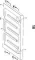
图1是一衬底的透视图,其中形成有一呈凹陷部的凹槽;1 is a perspective view of a substrate in which a groove is formed as a depression;
图2是沿图1线(II)-(II)在厚度方向的剖视图;Fig. 2 is a sectional view in the thickness direction along Fig. 1 line (II)-(II);
图3是沿图1线(III)-(III)在厚度方向的剖视图;Fig. 3 is a sectional view in the thickness direction along Fig. 1 line (III)-(III);
图4是将与图1所示之衬底结合在一起的一衬底的透视图;Figure 4 is a perspective view of a substrate to be combined with the substrate shown in Figure 1;
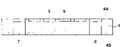
图5是沿图4线(V)-(V)在厚度方向的剖视图;Fig. 5 is a sectional view along the line (V)-(V) of Fig. 4 in the thickness direction;
图6是图4所示衬底的平面视图;Figure 6 is a plan view of the substrate shown in Figure 4;
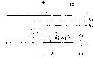
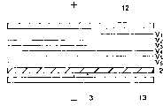
图7是表示一阳极连接的剖视图;Figure 7 is a cross-sectional view showing an anode connection;
图8示出了按照一比较的实施例与阳极连接相关之电场密度分配的图表;Figure 8 shows a graph of the electric field density distribution associated with the anode connection according to a comparative embodiment;
图9示出了按照本发明在阳极连接期间所述玻璃衬底薄膜之一前表面沿其厚度方向的组成;Figure 9 shows the composition of one of the front surfaces of the glass substrate film along its thickness direction during anodic bonding according to the present invention;
图10示出了按照本发明在阳极连接期间电场密度的分配;Figure 10 shows the distribution of the electric field density during anodic connection according to the invention;
图11示出了按照本发明在阳极连接期间一缓冲薄膜之一前表面沿其厚度方向的组成;Figure 11 shows the composition of a front surface of a buffer film along its thickness direction during anodic connection according to the present invention;
图12示出了按照本发明第二实施例之一阳极连接的剖视图;Figure 12 shows a cross-sectional view of an anode connection according to a second embodiment of the present invention;
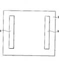
图13示出了按照本发明第二实施例之一衬底的平面视图;Figure 13 shows a plan view of a substrate according to a second embodiment of the present invention;
图14示出了按照本发明第三实施例之一阳极连接的剖视图;Figure 14 shows a cross-sectional view of an anode connection according to a third embodiment of the present invention;
图15示出了按照本发明第三实施例在阳极连接期间电场密度的分配;Figure 15 shows the distribution of electric field density during anodic connection according to a third embodiment of the present invention;
图16是一生产系统的框图,其中使用了按照本发明通过阳极连接技术得到的一个微反应器;Fig. 16 is a block diagram of a production system in which a microreactor obtained by anodic connection technique according to the present invention is used;
图17是所述生产系统中一生产模块的剖视图;以及Figure 17 is a sectional view of a production module in the production system; and
图18是所述生产系统的透视图。Fig. 18 is a perspective view of the production system.
具体实施方式Detailed ways
下面将参照附图对本发明之最佳实施方式予以描述。但是,本发明的范围并不局限于所示的实施例。DETAILED DESCRIPTION OF THE PREFERRED EMBODIMENTS The best mode for carrying out the present invention will be described below with reference to the accompanying drawings. However, the scope of the present invention is not limited to the shown embodiments.
第一实施例first embodiment
下面将就按照本发明将多个衬底连接在一起的方法的第一实施例予以描述。图1是将与另一个衬底相结合之一衬底的透视图。准确地说,所述衬底4包括如一个硅衬底或玻璃衬底,所述衬底具有一涂覆有一薄的导电薄膜的表面4A。所述衬底4具有一预定的厚度并且呈矩形。所述表面4A以及与其相反的面4B平直且彼此平行。所述衬底4具有一凹陷部5,所述凹陷部在所述表面4A上形成,并且具有呈迂回Z字形的凹槽。所述凹槽的一端形成有一个入口7以便于沿厚度方向贯穿所述衬底4。所述凹槽的另一端形成有一个出口8以便于沿厚度方向贯穿所述衬底4。流体由所述入口7流入并由所述出口8流出。A first embodiment of the method of joining together a plurality of substrates according to the present invention will be described below. Fig. 1 is a perspective view of a substrate to be combined with another substrate. More precisely, said
在处理所述衬底4之方法的第一个步骤中,一个预定的罩板被使用以构造所述凹陷部5,并通过诸如喷砂的机械蚀刻或使用一种蚀刻剂的化学蚀刻形成一个深度为0.1-1.5毫米的凹槽。类似的,所述凹槽的两端被机械或化学蚀刻以形成构成所述入口7以及所述出口8的通孔。如果所述衬底4采用玻璃,则可以在所述表面4A上形成一氧化薄膜以便于如下所述在一阳极连接期间被氧化。在这种情形下,所述氧化薄膜上涂覆有一保护薄膜,以防当所述凹陷部5、入口7以及出口8形成时其被氧化。图2是沿图1线(II)-(II)在所述衬底4厚度方向的剖视图。图3是沿图1线(III)-(III)在所述衬底4厚度方向的剖视图。In the first step of the method of processing the
如图4所示,将与所述衬底4结合在一起的玻璃衬底1具有覆盖其整个表面1A的缓冲薄膜2。一个迂回的阻热薄膜3位于所述缓冲薄膜2的一个前表面上。所述玻璃衬底1的一相反面与所述衬底4之所述表面4A阳极连接在一起。As shown in FIG. 4, the
如同所述衬底4的情形,所述玻璃衬底1的所述表面1A以及1B平直并且彼此平行,同时所述整个表面1B抵靠所述衬底4之所述表面4A。具体地说,所述玻璃衬底1由Pyrex(注册商标)构成,其含有百分之几的二氧化钠或苏打-石灰玻璃。图5是沿图4线(V)-(V)在所述衬底1之厚度方向的剖视图。所述缓冲薄膜2较所述阻热薄膜3具有一较大的薄膜形成区域。As in the case of the
处理所述玻璃衬底1之方法的第一步骤包括:在所述玻璃衬底1的所述底面形成所述缓冲薄膜2以便于覆盖整个底面。所述缓冲薄膜2被设置成其表面电阻(表面电阻率)大于所述阻热薄膜3之所述表面电阻,具体地说,表面电阻被设定为1-1000MΩ/□,这样的一种具有高电阻并且阳极连接期间在高温下不会衰减的材料可以是由钽、硅以及氧组成的化合物(在下面被称作钽-硅-氧基材料),或者是一种由钽、硅氧以及氮组成的化合物(在下面被称作钽-硅-氧-氮基材料)。The first step of the method of processing the
为了形成缓冲薄膜2,首先,所述玻璃衬底1被放置在一个喷镀装置中作为一将被涂覆的目标体。随后,其中埋有硅的一块钽板(钽∶硅=3∶1)被用作一个一目标体,以便于在由氩气以及氧气组成的大气环境中实施喷镀。在所述喷镀步骤中,粒子与所述目标体碰撞,从而使得所述目标体发出第二种离子。所述发出的第二种离子与所述玻璃衬底1的底面碰撞,从而在所述玻璃衬底1之所述底面上形成材质为钽-硅-氧基材料的缓冲薄膜2。如果被加工的是一种钽-硅-氧-氮基材料,则由钽板构成并且其中预埋硅的目标体可以在含有氩气、氧气以及氮气的大气环境中使用。To form the
所述缓冲薄膜2一旦形成,则在施加一电压而得以被加热的迂回状的阻热薄膜3在所述缓冲薄膜2的一个前表面上形成。所述形成的阻热薄膜3较所述缓冲薄膜2具有一较低的表面电阻,并且所述表面电阻的值最好等于或小于所述缓冲薄膜2之表面电阻的千分之一。如果所述缓冲薄膜2由钽-硅-氧基材料加工而成,则阻热薄膜3例如可以由表面电阻为100-1000MΩ/□的钽-硅-氧基材料加工而成。如果所述缓冲薄膜2由钽-硅-氧-氮基材料加工而成,则阻热薄膜3可以由诸如铜或铂的表面电阻为0.01-1MΩ/□的金属材料加工而成。Once the
利用钽-硅-氧基材料加工形成阻热薄膜3的方法和用于形成缓冲薄膜2的方法几乎相同。即,一块其中预埋有硅的钽板(钽∶硅=3∶1)被作为目标体。随后一玻璃衬底1被放置在一喷镀装置中以便于涂覆缓冲薄膜2。接着,在含有氩气、氧气以及氮气的大气环境中实施喷镀,同时使用具有一迂回状开口的罩板覆盖所述缓冲薄膜2。The method for forming the heat-resistant
在形成所述阻热薄膜3的步骤中,公知的影印石板术可被使用以便于在所述缓冲薄膜2的底面上形成所述阻热薄膜3。接着,所述阻热薄膜3可以被加工出迂回的图案。In the step of forming the heat-
在所述阻热薄膜3被加工之处,当所述玻璃衬底1与其中形成有迂回状凹陷部5的衬底4结合时,所述阻热薄膜3可沿着所述凹陷部而形成相应的迂回图案。此外,如果所述阻热薄膜3的形成用以覆盖所述凹陷部5,则其可以是矩形或其他的形状。所述玻璃衬底1以及所述衬底4一旦结合在一起,则所述凹陷部5可以起到便于由一种或多种材料混合物构成的流体流过之通道的功用。在这种情形下,当所述阻热薄膜3沿着所述凹陷部5迂回时,所述凹陷部5之通道的内部可以被均匀且有效地加热。所述阻热薄膜3最好较所述凹陷部5之相应的部分宽。Where the heat-blocking
形成所述阻热薄膜3的步骤使得所述薄膜3呈大致为迂回状的图案,这样一来,多个各具有一预定长度以及宽度的纵向部分3a如图6所示通过横向部分3b连接在一起。所述纵向部分3a垂直于所述横向部分3b而延伸。The step of forming the heat-
在此,所述阻热薄膜3之每一纵向部分3a的表面电阻被定义为Sh。所述每一纵向部分3a的宽度被定义为LA。所述每一纵向部分3a的长度被定义为LB。相邻之纵向部分之间的间隔被定义为LC。由所述两个纵向部分3a之间暴露的所述缓冲薄膜2部分的表面电阻被定义为Sf。则在平行于所述阻热薄膜3之所述横向部分3b的一直线上的两个部分X1、X2之间的所述阻热薄膜3部分的电阻通常满足Sh×(LB/LA)×2。所述两个部分X1、X2之间的所述缓冲薄膜2部分的电阻通常满足Sf×(LC/LB)。Here, the surface resistance of each
在所述第一实施例中,所述缓冲薄膜2以及所述阻热薄膜3最好在所述玻璃衬底1上形成以便于所述两个相邻之纵向部分3a的电阻以及由所述两个纵向部分3a之间暴露的所述缓冲薄膜2部分的电阻满足如下的等式(1):In the first embodiment, the
Sh×(LB/LA)×2×100<Sf×(LC/LB) (1)Sh×(LB /LA )×2×100<Sf×(LC /LB ) (1)
所述缓冲薄膜2以及所述阻热薄膜3基于等式(1)而在所述玻璃衬底1上形成,从而使得所述阻热薄膜3位于所述两个部分X1、X2之间部分的电阻等于或小于位于所述两个部分X1、X2之间的所述缓冲薄膜2之电阻的千分之一。随后,当一电压作用于所述阻热薄膜3之两端3c以及3d之间时,电流决不会流过位于所述两个部分X1、X2之间且较所述阻热薄膜3具有一较短的最小距离的所述缓冲薄膜2部分。另一方面,一电流可以流过所述阻热薄膜3,从而使其受到充分的加热。The
其中形成有凹陷部5的衬底4以及其上形成有缓冲薄膜2以及阻热薄膜3的玻璃衬底1一旦制备而成,则下面将要描述的如图7所示的步骤将得以实施。所述衬底4的表面4A抵靠所述玻璃衬底1的顶面1B(与形成有缓冲薄膜2以及阻热薄膜3之表面相反的面)。一阳极连接装置11之一正电极12与所述衬底4之所述表面4B相连以便于所述衬底4作为一阳极而工作。此时,所述衬底1以及所述缓冲薄膜2未与一负电极13直接接触。在这种状态下,所述衬底1以及4被加热至300-500℃。随后,所述阳极连接装置11向所述衬底1及4施加一300-1000伏的电压以将两者阳极连接在一起。此时,所述负电极13与包括纵向部分3a以及横向部分3b的所述阻热薄膜3之整个表面接触,以便于使得与所述玻璃衬底1接触的区域最大化。这样一来,靠近所述玻璃衬底1之所述表面1A的氧原子与在所述衬底4之所述表面4A上的原子化学结合在一起,从而使得衬底4以及所述玻璃衬底1结合在一起。在经过阳极连接之后,电极连接装置位于所述阻热薄膜3之相应的端部3c以及3d处。所述电极连接装置包括三层,即作为底层的钨-钛层,作为中间层的金层以及作为顶层的钛层。Once the
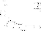
当所述缓冲薄膜2被形成而覆盖所述玻璃衬底1之整个底面,并且所述玻璃衬底1以及所述衬底4被阳极连接在一起时,阳极连接装置11之所述负电极的电场穿过所述阻热薄膜3并且在所述缓冲薄膜2中大范围地扩散。所述玻璃衬底1以及所述衬底4之间的阳极连接将在下面予以描述。在其中未形成一缓冲薄膜2的比较实施例中,等位线LV1-LV7(其中电压值按照LV1,LV2,LV3,LV4,LV5以及LV6的顺序增大)按照一小的间隔排列,同时所述电场密度如图8所示在所述玻璃衬底1之靠近与所述阳极连接装置11之所述负电极13相接触之阻热薄膜3的部分集中。所述电场使得所述钠离子由所述玻璃衬底1移动并使得所述离子局部沉积于所述表面1A之靠近所述阻热薄膜3的部分。但是,所述钠离子可沿厚度方向蚀刻所述阻热薄膜3。这就使得所述阻热薄膜3很难用作一个阻热器。图9示出了图8所示阳极连接之玻璃衬底1之所述前表面的组成。图示的所述组成可以通过RBS/HFS而得到。由该图可以看出,所述表面是富含钠的玻璃。此外,在所述前表面集中的氢来自水分子。沿所述玻璃衬底1的厚度方向具有相当大量的氢,因而其有可能导致蚀刻。When the
然而,在所述第一实施例中,具有一较大电阻并且较所述阻热薄膜3具有一较大宽度的缓冲薄膜2在所述玻璃衬底1以及所述阻热薄膜3之间形成。随后,所述阳极连接装置11之所述正电极12以及所述负电极13之间电场密度的偏移得以抑制,同时所述等位线LV1-LV7的间隔如图10所示几乎是一致的。图11示出了图10所示阳极连接之玻璃衬底1之所述前表面的组成,图示的所述组成可以通过RBS/HFS而得到。由该图可以看出,与上相比,靠近所述缓冲薄膜2之所述前表面的钠的比率减少。如此一来,所述缓冲薄膜2的设置使得所述玻璃衬底1中所含有的钠局部沉积于所述玻璃衬底1之所述底面上。此外,所述缓冲薄膜2之所述钽-硅-氧基材料具有适当的密集结构。相应地,所述缓冲薄膜2自身在某种程度上可起到阻止所述钠移动的屏障作用并且可以吸收钠。因此,钠不会在靠近所述玻璃衬底1之所述表面1A的界面处局部出现。此外,所述钠的集中不会非常的靠近所述阻热薄膜3,即所述缓冲薄膜2之所述前表面。这相应的有阻止了在所述缓冲薄膜2上形成之所述阻热薄膜3由于钠的存在而变脆。这因此就使得防止所述阻热薄膜3由所述玻璃衬底1上剥落成为可能。此外,氢沿所述阻热薄膜3之所述厚度方向的集中程度相当的低。这表明水被阻止进入所述玻璃衬底1。因此这就有可能阻止水对作为一微反应器之所述玻璃衬底1中反应的影响。However, in the first embodiment, the
在所述第一实施例之形成所述缓冲薄膜2的步骤中,喷镀在体积上包括99%的氩气以及1%的氧气并且压力为10托的大气环境中实施,以便于形成表面电阻值Sh为1000MΩ/□的缓冲薄膜2。In the step of forming the
在形成阻热薄膜3的步骤中,所述每一纵向部分3a的宽度LA为100微米,长度LB为4000微米,表面电阻Sh为0.5MΩ/□,并且相邻之所述纵向部分3a之间的间隔Lc为100微米。In the step of forming the heat-
在这种情况下,所述每一纵向部分3a的表面电阻Sh×(LB×LA)为0.5MΩ/□×4000/100微米=20欧(Ω)。由所述纵向部分3a之间暴露的所述缓冲薄膜2部分的电阻Sf×(LA×LB)为1000MΩ/□×100/4000微米=25千欧。In this case, the surface resistance Sh*(LB *LA ) of each
因此,由所述纵向部分3a之间暴露的所述缓冲薄膜2部分的电阻(25千欧)远远大于电阻20×2=40欧;准确地说,将相邻两个纵向部分3a相连在一起的一个横向部分3b的电阻应当为所述阻热薄膜3之所述两个纵向部分3a之电阻的和。因而上述的等式(1)得到满足。Therefore, the resistance (25 kiloohms) of the
在这种状态下,当一电压施加于所述阻热薄膜3的两端3c以及3d之间时,所述呈迂回图案之阻热薄膜3能够被有效地加热,同时流过所述缓冲薄膜2之电流的过流能够得以抑制。In this state, when a voltage is applied between the two ends 3c and 3d of the heat-
在所述第一实施例中,所述阳极连接仅仅通过所述阳极连接装置11之所述负电极13与所述热阻薄膜3的接触而得以实施。但是,本发明并不局限于这一方面。所述阳极连接也可通过所述负电极与所述阻热薄膜3以及所述缓冲薄膜2之所述暴露部分的接触而得以实现。In the first embodiment, the anode connection is implemented only through the contact between the
(第二实施例)(second embodiment)
下面将对按照本发明之将衬底连接在一起之方法的第二实施例予以说明。在所述第二实施例中,与第一实施例类似的部件采用相同的图标记。同时对这些部件相应的描述将省略。Next, a second embodiment of the method of joining substrates together according to the present invention will be described. In said second embodiment, parts similar to those of the first embodiment bear the same reference numerals. Meanwhile, corresponding descriptions of these components will be omitted.
首先如图12所示,所述玻璃衬底1被制备。喷镀如同第一实施例所述被实施以便于在所述玻璃衬底1之所述底面上形成钽-硅-氧-氮基材料或类似材料的阻热薄膜3。但是。在所述薄膜形成步骤中,所述矩形阻热薄膜3被形成以覆盖所述玻璃衬底1之整个底面(具体地说,所述阻热薄膜3必须覆盖所述玻璃衬底1之所述底面的80%或更多)而不是形成迂回状的图案。所述阻热薄膜3之所述表面电阻值至少为100MΩ/□。First, as shown in FIG. 12 , the
所述阻热薄膜3一经在所述玻璃衬底1之所述表面1A上形成,则一对互连件6如图13所示在所述阻热薄膜3的所述前表面上形成。所述互连件6用作一电极连接件,据此动力能够提供给所述阻热薄膜3。所述每一互连件6由三金属层组成,即钨-钛层/金层/钨-钛层。所述钨-钛是钨钛合金,其与钽-硅-氧基,钽-硅-氧-氮基、其他金属氧化物以及诸如金的金属相连。钨钛用作金的底部保护薄膜。金是一低电阻材料并且用作所述互连件之主要部分。金未和所述金属氧化物相连但是可以与钨钛良好的连接。所述互连件的电阻低于所述阻热薄膜3的电阻,最好等于或小于所述阻热薄膜3之所述电阻值的1/100。所述互连件6用作向所述阻热薄膜3提供动力之电极的主要部分。Once the heat-
所述互连件6与第一实施例一样通过公知的影印石板术、蚀刻以及/或喷镀处理而得以形成。所述互连件6一经形成,则长边相对并且彼此远离的呈直线状的互连件6分别位于所述衬底1的左右位置处,从而使得所述阻热薄膜3上的整个凹陷部5在所述玻璃衬底1以及所述衬底4结合在一起之后能够被充分的加热。所述互连件6之间的最短距离在任何位置均是相同的。因此,当一电压作用于所述互连件6之间时,位于所述互连件6之间的所述阻热薄膜3能够被均匀且有效地加热。The
一侧形成有阻热薄膜3以及互连件6的玻璃衬底1以及所述衬底4一经被制备,下述的如图12所示的步骤将被实施。首先,所述玻璃衬底1之与形成有所述阻热薄膜3之表面1A相反的面1B抵靠其上形成有所述凹陷部或凹槽5的衬底4的表面4A。随后,所述衬底4的表面4B与所述阳极连接装置11之所述正电极12相连,同时所述阳极连接装置11之所述负电极13与所述互连件6相连。一阳极连接得以实施从而将所述玻璃衬底1以及所述衬底4连接在一起。由于第一实施例中的缓冲薄膜2为阻热薄膜3所替代,同时第一实施例中的阻热薄膜3为所述互连件6所取代,因此玻璃衬底1上的电场在靠近互连件6处的集中得以控制,故所述阻热薄膜3起到一缓冲薄膜的作用。所述玻璃衬底1中的钠均匀地在所述阻热薄膜3中分布。这就使得减少钠在所述互连件6中以及靠近所述互连件6的所述阻热薄膜3之前表面上的集中成为可能。Once the
所述阳极连接装置11之所述负电极13可以选择性地只与所述阻热薄膜3的前表面相连而不是如上所述仅与所述互连件6相连。另外,所述阳极连接装置11之所述负电极13可以与所述阻热薄膜3以及所述互连件6两者均相连。在任何一种方式下,在所述玻璃衬底1以及所述衬底4阳极连接在一起之前,当所述阻热薄膜3形成并覆盖整个表面1A时,所述阳极连接装置11之所述负电极13的电场在所述阻热薄膜3中大范围地分布。这就与第一实施例一样可以避免所述阳极连接装置11之所述正电极12以及负电极13之间电场的局部集中。因此,所述玻璃衬底1厚度方向的电场密度是均匀的,从而避免了电场分布的偏移。这样一来,在第二实施例中,玻璃衬底1中钠的局部沉积可得以控制。此外,呈直线状的用于提供动力的互连件6由所述玻璃衬底1上的脱落也可得以控制。The
(第三实施例)(third embodiment)
下面将对按照本发明之将衬底连接在一起之方法的第三实施例予以说明。在所述第三实施例中,与第一以及第二实施例类似的部件采用相同的图标记。同时对这些部件相应的描述将省略。Next, a third embodiment of the method of joining substrates according to the present invention will be described. In said third embodiment, parts similar to those of the first and second embodiments bear the same reference numerals. Meanwhile, corresponding descriptions of these components will be omitted.
首先制备所述玻璃衬底1。随后如同第一实施例,在所述玻璃衬底1之整个表面1A上形成由钽-硅-氧基材料构成的缓冲薄膜2。所述缓冲薄膜2一经形成,则下述的如图14所示的步骤将被实施。如同第二实施例所述,由钽-硅-氧-氮基材料构成的阻热薄膜3在所述缓冲薄膜2之整个前表面形成。因此,与所述第二实施例相同,一对互连件6如图13所示在所述阻热薄膜3的前表面形成,并且其长边彼此相对,其中所述互连件包括三金属层,即作为基础层的钨钛层,作为中间层的金层以及作为顶层的钛层。所述每一互连件6较所述缓冲薄膜2以及阻热薄膜3聚于一较小的表面电阻。Firstly, the
其上形成有所述阻热薄膜3的玻璃衬底1以及衬底4一经制备好后,则下述的如图14所示的步骤将被实施。首先,所述玻璃衬底1之与形成有所述阻热薄膜3之表面1A相反的面1B抵靠其上形成有所述凹陷部或流体通道5的衬底4的表面4A。随后,所述衬底4的表面4B与所述阳极连接装置11之所述正电极12相连,同时所述阳极连接装置11之所述负电极13与所述互连件6相连。一阳极连接得以实施从而将所述玻璃衬底1以及所述衬底4连接在一起。所述阻热薄膜3起到一缓冲薄膜的作用。相应地,如图15所示,所述玻璃衬底1表面方向的电场分布是均匀的并且其在靠近所述互连件6的部分不会产生电场集中。所述玻璃衬底1中的钠均匀地在所述阻热薄膜3中分布。这就使得减少钠在所述互连件6中以及靠近所述互连件6的所述阻热薄膜3之前表面上的集中成为可能。所述互连件6由所述阻热薄膜3上的脱落可得以控制。同时所述互连件6由所述缓冲薄膜2上的脱落也能够得以控制。Once the
在第三实施例中,阳极连接可通过负电极13仅与其上无互连件6的所述阻热薄膜3之所述前表面的接触而实施。另外,所述阳极连接也可通过所述负电极13与所述阻热薄膜3以及所述互连件6两者的接触而实施。In the third embodiment, the anodic connection can be carried out by the contact of the
在第一至第三实施例中,所述凹陷部5仅在所述衬底4上形成以便于为使得化学反应得以发生之材料的流动提供一通道。但是,本发明并不局限于此,所述凹陷部5也可只在所述玻璃衬底1上形成。另外,也可在所述玻璃衬底1以及衬底4上形成相对的凹陷部,由两个凹陷部形成一通道。In the first to third embodiments, the recessed
第一至第三实施例中的接合衬底(使用按照本发明第一至第三实施例之连接方法生产的玻璃衬底1以及衬底4的结合单元(包括缓冲薄膜2、阻热薄膜3以及互连件6))可用作被成为微反应器的一个精细的反应器。特别地,一材料系统中的流体可以流过由所述凹陷部5构成且深度大约为0.01-0.02毫米的通道。随后,所述阻热薄膜3可用于加热所述通道以使得其中发生化学反应。这种接合衬底可用作一微反应器,其重组诸如二乙醚或甲醇的碳氢化合物而提取氢。特别地,其可由有效地用作一使得呈固态或液态的碳氢化合物蒸发的浓缩微反应器,一将碳氢化合物重组至氢中的氢重组微反应器,去除一氧化碳的微反应器。因此,所述接合衬底有助于减少通过与水的化学反应而产生动力之燃料电池的尺寸。Bonded substrates in the first to third embodiments (using the bonding unit of the
图16示出了一微重组器的实施例,其中应用了一个微反应器,所述微反应器采用了如上所述通过阳极连接技术结合在一起衬底1及4,所述为重组器将一种燃料重组至供给一燃料电池的氢。Fig. 16 shows an embodiment of a microrecombiner, wherein a microreactor is applied, and the microreactor adopts the
将通过微重组器而重组至水中的甲醇以及水密闭在一个燃料箱21中。Methanol recombined into water by the microrecombiner and water are sealed in a
燃料蒸发器22是一微重组器,如图17所示,其利用内阻热薄膜3加热图17所示之燃料箱21提供的水及甲醇的混合液并使其蒸发。The
氢重组器23是一微重组器,其按照如下的方程式使得一氢重组反应得以产生,从而重组由燃料蒸发器22提供的被蒸发的甲醇及水:The hydrogen recombiner 23 is a microrecombiner that enables a hydrogen recombination reaction to be generated to recombine the vaporized methanol and water provided by the
CH3OH+H2O→3H2+CO2 (2)CH3OH +H2O →3H2 +CO2 (2 )
一个一氧化碳去除装置24是一微重组器,其将一氧化碳氧化成二氧化碳,一氧化碳是氢重组器23中产生之反应的副产品,同时该反应中还产生氢气,如下面的反应式(3)及(4)所示:A carbon
CO+H2O→CO2+H2 (3)CO+H2O →CO2 +H2 (3)
CO+(1/2)O2→CO2 (4)CO+(1/2)O2 →CO2 (4)
如图17所示,一燃料电池25具有一氢柱34,所述氢柱使得一电化学反应得以产生,其将经由一氧化碳去除装置24通过氢重组器23产生的氢气分解成氢离子以及电子,在所述氢柱以及一氧柱之间具有一能够使得所述氢离子得以通过的氢离子传输薄膜36,所述单元还包括氧柱,所述氧柱使得被吸收的氧以及经由氢离子传输薄膜传输的氢离子及电子之间发生电化学反应。燃料箱基于上述一系列的电化学反应而产生动力。As shown in FIG. 17, a
下面将对生成模块101予以说明,所述模块包括燃料蒸发器22,氢重组器23,一氧化碳去除装置24以及燃料电池25。The
所述燃料蒸发器22,氢重组器23以及一氧化碳去除装置24的上侧以及下侧均通过阻热固定薄膜28而固定,其周向为阻热格26所分隔。所述阻热格26与所述燃料蒸发器22,氢重组器23以及一氧化碳去除装置24中每一个之间的间隔的设定使得一惰性气体环境的压力减少至1托或更低。因此,来自所述内部阻热薄膜3及类似部件的热量得以传输至衬底1及4。所述间隔中仅仅包含少量的用于传输热的介质,从而对流几乎不发生并能够得到最小的热损。The upper and lower sides of the
所述氢重组器23具有一催化剂层27,所述催化剂层27利用涂覆于所述凹陷部5之壁面上的氧化铝或类似材料来构成一使得反应式(2)得以进行的铜/氧化锌基催化剂。所述一氧化碳去除装置24具有一催化剂层27,所述催化剂层27利用涂覆于所述凹陷部5之壁面上的氧化铝或类似材料来构成一使得反应式(4)得以进行的铂催化剂。Described
位于所述燃料蒸发器22、氢重组器23以及一氧化碳去除装置24中的阻热薄膜3将所述凹陷部5中的流体分别加热至120℃、280℃以及190℃,以利于蒸发反应以及/或化学反应。The heat-
所述燃料蒸发器22之所述凹陷部5的一端具有一流入管29,所述流入管接收来自所述燃料箱21的燃料,一个流入管30与和所述燃料蒸发器22之所述凹陷部5的另一端连通的所述氢重组器23之所述凹陷部5相连以吸入诸如被蒸发之甲醇的气体。与所述燃料蒸发器22之所述凹陷部5的另一端连通的所述一氧化碳去除装置24之所述凹陷部5的一端具有一流入管31以吸入气体,诸如通过化学反应生成的氢气。所述一氧化碳去除装置24之所述凹陷部5的另一端具有一流出管32排出其中的一氧化碳已被去除并富含氢气的气体。所述流出管32所述流入管33的一段相连,据此来自所述流出管32的氢气被吸入。所述流入管33的另一端与所述燃料电池25相连。所述燃料电池25环绕所述燃料蒸发器22,氢重组器23以及一氧化碳去除装置24的周向。如上所述,所述燃料电池25具有氢柱34,氧柱35以及介于所述氢柱以及氧柱之间的氢离子输送薄膜36。所述单元还包括一个收集板37,所述收集板与所述氢柱34电连接,并与所述流入管33相连,同时具有一个废气排出口42,所述单元还具有一个与所述氧柱35电连接并且具有多个吸氧口39的收集板38。One end of the recessed
所述生成模块101包括一个用于放置所述燃料蒸发器22,氢重组器23,一氧化碳去除装置24以及所述燃料电池25的箱体40。所述箱体40具有多个与所述吸氧口39相通的狭缝41以及多个与所述废气排出口42相通的排出口43。The
所述氧柱35以及所述收集板38之间具有一个排出管44用以排出由动力生成所产生的水。A
图18是与所述燃料箱21相连之所述生成模块101的透视图。所述燃料箱21具有一个燃料包52,其中密闭有包括水以及诸如甲醇之酒精的燃料。FIG. 18 is a perspective view of the
所述燃料包52位于一保护箱46中,所述保护箱46具有一窗子47以便于部分暴露。所述保护箱46用作所述燃料箱21以及所述生成模块101之间的分界。所述保护箱46具有一个吸管48,据此由所述排出管44排出的水被吸入。The
当所述燃料包52被安装至位于所述生成模块101中的所述保护箱46中时,所述流入管29被插入所述燃料包52被为燃料所充满。相应地,燃料51可通过所述流入管29而被吸入。When the
所述生成模块101通过使用由阳极连接而生产的作为一微反应器的薄的燃料蒸发器22,氢重组器23以及一氧化碳去除装置24,整个结构之尺寸的减小成为可能。The
Claims (29)
Translated fromChineseApplications Claiming Priority (2)
| Application Number | Priority Date | Filing Date | Title |
|---|---|---|---|
| JP2003299742AJP4380264B2 (en) | 2003-08-25 | 2003-08-25 | Bonding substrate and substrate bonding method |
| JP299742/2003 | 2003-08-25 |
Publications (2)
| Publication Number | Publication Date |
|---|---|
| CN1744944A CN1744944A (en) | 2006-03-08 |
| CN100393409Ctrue CN100393409C (en) | 2008-06-11 |
Family
ID=34213777
Family Applications (1)
| Application Number | Title | Priority Date | Filing Date |
|---|---|---|---|
| CNB2004800031216AExpired - Fee RelatedCN100393409C (en) | 2003-08-25 | 2004-08-12 | Bonding substrates and method of bonding substrates together |
Country Status (8)
| Country | Link |
|---|---|
| US (2) | US7205625B2 (en) |
| EP (1) | EP1658132A1 (en) |
| JP (1) | JP4380264B2 (en) |
| KR (1) | KR100671322B1 (en) |
| CN (1) | CN100393409C (en) |
| CA (1) | CA2509912C (en) |
| TW (1) | TWI296266B (en) |
| WO (1) | WO2005018798A1 (en) |
Families Citing this family (15)
| Publication number | Priority date | Publication date | Assignee | Title |
|---|---|---|---|---|
| US7470142B2 (en)* | 2004-06-21 | 2008-12-30 | Sang-Yun Lee | Wafer bonding method |
| WO2005090227A1 (en)* | 2004-03-23 | 2005-09-29 | Casio Computer Co., Ltd. | Stack structure and method of manufacturing the same |
| KR100623177B1 (en)* | 2005-01-25 | 2006-09-13 | 삼성전자주식회사 | Dielectric structure having high dielectric constant, manufacturing method thereof, nonvolatile semiconductor memory device comprising same and manufacturing method thereof |
| KR100691274B1 (en)* | 2005-08-24 | 2007-03-12 | 삼성전기주식회사 | Thin type reformer |
| JP5320657B2 (en)* | 2005-09-20 | 2013-10-23 | カシオ計算機株式会社 | Bonding substrate and bonding method |
| KR100674863B1 (en)* | 2005-09-29 | 2007-01-29 | 삼성전기주식회사 | Thin type reformer |
| KR100818761B1 (en)* | 2006-08-16 | 2008-04-01 | (주) 비앤피 사이언스 | Electrode Intermediate Module for Anode Bonding Chamber and Anode Bonding Method Using the Same |
| JP5529463B2 (en)* | 2009-08-25 | 2014-06-25 | セイコーインスツル株式会社 | Package manufacturing method and piezoelectric vibrator manufacturing method |
| JP2012169376A (en)* | 2011-02-10 | 2012-09-06 | Seiko Instruments Inc | Positive electrode junction device, package manufacturing method, piezoelectric vibrator, oscillator, electronic apparatus, and radio controlled clock |
| JP5791322B2 (en)* | 2011-03-28 | 2015-10-07 | セイコーインスツル株式会社 | Package manufacturing method |
| JP6405767B2 (en)* | 2014-07-24 | 2018-10-17 | 住友電気工業株式会社 | Gallium nitride substrate |
| CN105589587B (en)* | 2014-10-21 | 2018-10-26 | 宸鸿科技(厦门)有限公司 | Transparent composite substrate and preparation method and touch panel |
| CN104860549A (en)* | 2015-04-20 | 2015-08-26 | 安徽立光电子材料股份有限公司 | Electric heating conductive glass and manufacturing method thereof |
| CN104860548B (en)* | 2015-06-08 | 2017-09-26 | 东莞鑫泰玻璃科技有限公司 | A kind of preparation method of infrared external reflection antireflection coating glass |
| CN107352504A (en)* | 2017-06-07 | 2017-11-17 | 扬中市华瑞通讯仪器有限公司 | A kind of micro-fluidic MEMS chip method for packing |
Citations (3)
| Publication number | Priority date | Publication date | Assignee | Title |
|---|---|---|---|---|
| US4826787A (en)* | 1986-03-18 | 1989-05-02 | Fujitsu Limited | Method for adhesion of silicon or silicon dioxide plate |
| EP0742851A1 (en)* | 1994-12-02 | 1996-11-20 | B a r m a g AG | Spinning beam for spinning a plurality of synthetic threads and spinning device comprising a spinning beam of this type |
| US5639423A (en)* | 1992-08-31 | 1997-06-17 | The Regents Of The University Of Calfornia | Microfabricated reactor |
Family Cites Families (12)
| Publication number | Priority date | Publication date | Assignee | Title |
|---|---|---|---|---|
| DE69233314T2 (en)* | 1991-10-11 | 2005-03-24 | Canon K.K. | Process for the production of semiconductor products |
| DE4136075C3 (en) | 1991-10-30 | 1999-05-20 | Siemens Ag | Method for connecting a disk-shaped insulating body to a disk-shaped, conductive body |
| US5591679A (en) | 1995-04-12 | 1997-01-07 | Sensonor A/S | Sealed cavity arrangement method |
| DE19707044C1 (en) | 1997-02-21 | 1998-08-06 | Inst Physikalische Hochtech Ev | Microflow module for calorimetric measurements |
| US6016027A (en)* | 1997-05-19 | 2000-01-18 | The Board Of Trustees Of The University Of Illinois | Microdischarge lamp |
| US6172385B1 (en)* | 1998-10-30 | 2001-01-09 | International Business Machines Corporation | Multilayer ferroelectric capacitor structure |
| JP3729011B2 (en) | 2000-02-14 | 2005-12-21 | セイコーエプソン株式会社 | Microreactor |
| JP3906653B2 (en)* | 2000-07-18 | 2007-04-18 | ソニー株式会社 | Image display device and manufacturing method thereof |
| US6426525B1 (en)* | 2001-04-18 | 2002-07-30 | Tyco Electronics Corporation | FET structures having symmetric and/or distributed feedforward capacitor connections |
| DE10200399B4 (en)* | 2002-01-08 | 2008-03-27 | Advanced Micro Devices, Inc., Sunnyvale | A method for producing a three-dimensionally integrated semiconductor device and a three-dimensionally integrated semiconductor device |
| JP3891131B2 (en) | 2002-03-29 | 2007-03-14 | カシオ計算機株式会社 | Chemical reaction apparatus and power supply system |
| US7169367B2 (en)* | 2002-04-05 | 2007-01-30 | Casio Computer Co., Ltd. | Chemical reaction apparatus and power supply system |
- 2003
- 2003-08-25JPJP2003299742Apatent/JP4380264B2/ennot_activeExpired - Fee Related
- 2004
- 2004-08-11USUS10/916,203patent/US7205625B2/ennot_activeExpired - Fee Related
- 2004-08-12CACA002509912Apatent/CA2509912C/ennot_activeExpired - Fee Related
- 2004-08-12KRKR1020057012898Apatent/KR100671322B1/ennot_activeExpired - Fee Related
- 2004-08-12EPEP04771824Apatent/EP1658132A1/ennot_activeWithdrawn
- 2004-08-12CNCNB2004800031216Apatent/CN100393409C/ennot_activeExpired - Fee Related
- 2004-08-12WOPCT/JP2004/011863patent/WO2005018798A1/enactiveIP Right Grant
- 2004-08-25TWTW093125425Apatent/TWI296266B/ennot_activeIP Right Cessation
- 2007
- 2007-02-22USUS11/677,859patent/US7867346B2/ennot_activeExpired - Fee Related
Patent Citations (3)
| Publication number | Priority date | Publication date | Assignee | Title |
|---|---|---|---|---|
| US4826787A (en)* | 1986-03-18 | 1989-05-02 | Fujitsu Limited | Method for adhesion of silicon or silicon dioxide plate |
| US5639423A (en)* | 1992-08-31 | 1997-06-17 | The Regents Of The University Of Calfornia | Microfabricated reactor |
| EP0742851A1 (en)* | 1994-12-02 | 1996-11-20 | B a r m a g AG | Spinning beam for spinning a plurality of synthetic threads and spinning device comprising a spinning beam of this type |
Also Published As
| Publication number | Publication date |
|---|---|
| US20050046007A1 (en) | 2005-03-03 |
| KR100671322B1 (en) | 2007-01-19 |
| US7867346B2 (en) | 2011-01-11 |
| CA2509912A1 (en) | 2005-03-03 |
| JP4380264B2 (en) | 2009-12-09 |
| TW200513452A (en) | 2005-04-16 |
| JP2005067951A (en) | 2005-03-17 |
| CN1744944A (en) | 2006-03-08 |
| EP1658132A1 (en) | 2006-05-24 |
| WO2005018798A1 (en) | 2005-03-03 |
| KR20060032581A (en) | 2006-04-17 |
| TWI296266B (en) | 2008-05-01 |
| CA2509912C (en) | 2009-02-24 |
| US20070181249A1 (en) | 2007-08-09 |
| US7205625B2 (en) | 2007-04-17 |
Similar Documents
| Publication | Publication Date | Title |
|---|---|---|
| CN100393409C (en) | Bonding substrates and method of bonding substrates together | |
| US7858261B2 (en) | Systems and methods for stacking fuel cells | |
| KR101019162B1 (en) | Reactor | |
| US8123825B2 (en) | Microreactor and production method thereof | |
| US20110041986A1 (en) | Micro-reactor and method of manufacturing the same | |
| JP3899985B2 (en) | Microreactor structure and manufacturing method thereof | |
| US7879298B2 (en) | Microreactor | |
| JP4504751B2 (en) | Microreactor for hydrogen production | |
| KR100821413B1 (en) | Stack structure and method of manufacturing the same | |
| CN100394638C (en) | Reactors and Power Plants | |
| JP2007207672A (en) | Thin film heater and manufacturing method thereof | |
| KR20030060668A (en) | A Separator with micro channel and thereof fabrication method | |
| JP4537685B2 (en) | Membrane reactor for hydrogen production | |
| JP5320657B2 (en) | Bonding substrate and bonding method | |
| KR100828489B1 (en) | Micro reactor and its manufacturing method | |
| CN100447073C (en) | Stack structure and manufacturing method thereof | |
| JP5309482B2 (en) | Reactor, power generator and electronic device | |
| JP2009160480A (en) | Manufacturing method of microreactor |
Legal Events
| Date | Code | Title | Description |
|---|---|---|---|
| C06 | Publication | ||
| PB01 | Publication | ||
| C10 | Entry into substantive examination | ||
| SE01 | Entry into force of request for substantive examination | ||
| C14 | Grant of patent or utility model | ||
| GR01 | Patent grant | ||
| CF01 | Termination of patent right due to non-payment of annual fee | ||
| CF01 | Termination of patent right due to non-payment of annual fee | Granted publication date:20080611 Termination date:20160812 |