CN100392891C - Organic electroluminescent element, method for manufacturing the same, and organic electroluminescent display device - Google Patents
Organic electroluminescent element, method for manufacturing the same, and organic electroluminescent display deviceDownload PDFInfo
- Publication number
- CN100392891C CN100392891CCNB2003101102998ACN200310110299ACN100392891CCN 100392891 CCN100392891 CCN 100392891CCN B2003101102998 ACNB2003101102998 ACN B2003101102998ACN 200310110299 ACN200310110299 ACN 200310110299ACN 100392891 CCN100392891 CCN 100392891C
- Authority
- CN
- China
- Prior art keywords
- light
- organic
- emitting layer
- mentioned
- manufacturing
- Prior art date
- Legal status (The legal status is an assumption and is not a legal conclusion. Google has not performed a legal analysis and makes no representation as to the accuracy of the status listed.)
- Expired - Lifetime
Links
Images


Classifications
- H—ELECTRICITY
- H05—ELECTRIC TECHNIQUES NOT OTHERWISE PROVIDED FOR
- H05B—ELECTRIC HEATING; ELECTRIC LIGHT SOURCES NOT OTHERWISE PROVIDED FOR; CIRCUIT ARRANGEMENTS FOR ELECTRIC LIGHT SOURCES, IN GENERAL
- H05B33/00—Electroluminescent light sources
- H05B33/10—Apparatus or processes specially adapted to the manufacture of electroluminescent light sources
- H—ELECTRICITY
- H10—SEMICONDUCTOR DEVICES; ELECTRIC SOLID-STATE DEVICES NOT OTHERWISE PROVIDED FOR
- H10K—ORGANIC ELECTRIC SOLID-STATE DEVICES
- H10K50/00—Organic light-emitting devices
- H10K50/80—Constructional details
- H10K50/84—Passivation; Containers; Encapsulations
- H10K50/842—Containers
- H10K50/8426—Peripheral sealing arrangements, e.g. adhesives, sealants
- H—ELECTRICITY
- H10—SEMICONDUCTOR DEVICES; ELECTRIC SOLID-STATE DEVICES NOT OTHERWISE PROVIDED FOR
- H10K—ORGANIC ELECTRIC SOLID-STATE DEVICES
- H10K50/00—Organic light-emitting devices
- H10K50/80—Constructional details
- H10K50/84—Passivation; Containers; Encapsulations
- H10K50/844—Encapsulations
- H—ELECTRICITY
- H10—SEMICONDUCTOR DEVICES; ELECTRIC SOLID-STATE DEVICES NOT OTHERWISE PROVIDED FOR
- H10K—ORGANIC ELECTRIC SOLID-STATE DEVICES
- H10K59/00—Integrated devices, or assemblies of multiple devices, comprising at least one organic light-emitting element covered by group H10K50/00
- H10K59/30—Devices specially adapted for multicolour light emission
- H10K59/35—Devices specially adapted for multicolour light emission comprising red-green-blue [RGB] subpixels
- H—ELECTRICITY
- H10—SEMICONDUCTOR DEVICES; ELECTRIC SOLID-STATE DEVICES NOT OTHERWISE PROVIDED FOR
- H10K—ORGANIC ELECTRIC SOLID-STATE DEVICES
- H10K59/00—Integrated devices, or assemblies of multiple devices, comprising at least one organic light-emitting element covered by group H10K50/00
- H10K59/80—Constructional details
- H10K59/87—Passivation; Containers; Encapsulations
- H10K59/873—Encapsulations
- C—CHEMISTRY; METALLURGY
- C09—DYES; PAINTS; POLISHES; NATURAL RESINS; ADHESIVES; COMPOSITIONS NOT OTHERWISE PROVIDED FOR; APPLICATIONS OF MATERIALS NOT OTHERWISE PROVIDED FOR
- C09K—MATERIALS FOR MISCELLANEOUS APPLICATIONS, NOT PROVIDED FOR ELSEWHERE
- C09K2323/00—Functional layers of liquid crystal optical display excluding electroactive liquid crystal layer characterised by chemical composition
- H—ELECTRICITY
- H10—SEMICONDUCTOR DEVICES; ELECTRIC SOLID-STATE DEVICES NOT OTHERWISE PROVIDED FOR
- H10K—ORGANIC ELECTRIC SOLID-STATE DEVICES
- H10K50/00—Organic light-emitting devices
- H10K50/80—Constructional details
- H10K50/86—Arrangements for improving contrast, e.g. preventing reflection of ambient light
- H10K50/865—Arrangements for improving contrast, e.g. preventing reflection of ambient light comprising light absorbing layers, e.g. light-blocking layers
- H—ELECTRICITY
- H10—SEMICONDUCTOR DEVICES; ELECTRIC SOLID-STATE DEVICES NOT OTHERWISE PROVIDED FOR
- H10K—ORGANIC ELECTRIC SOLID-STATE DEVICES
- H10K59/00—Integrated devices, or assemblies of multiple devices, comprising at least one organic light-emitting element covered by group H10K50/00
- H10K59/10—OLED displays
- H10K59/12—Active-matrix OLED [AMOLED] displays
- H—ELECTRICITY
- H10—SEMICONDUCTOR DEVICES; ELECTRIC SOLID-STATE DEVICES NOT OTHERWISE PROVIDED FOR
- H10K—ORGANIC ELECTRIC SOLID-STATE DEVICES
- H10K59/00—Integrated devices, or assemblies of multiple devices, comprising at least one organic light-emitting element covered by group H10K50/00
- H10K59/10—OLED displays
- H10K59/17—Passive-matrix OLED displays
- H10K59/173—Passive-matrix OLED displays comprising banks or shadow masks
- H—ELECTRICITY
- H10—SEMICONDUCTOR DEVICES; ELECTRIC SOLID-STATE DEVICES NOT OTHERWISE PROVIDED FOR
- H10K—ORGANIC ELECTRIC SOLID-STATE DEVICES
- H10K59/00—Integrated devices, or assemblies of multiple devices, comprising at least one organic light-emitting element covered by group H10K50/00
- H10K59/30—Devices specially adapted for multicolour light emission
- H10K59/35—Devices specially adapted for multicolour light emission comprising red-green-blue [RGB] subpixels
- H10K59/353—Devices specially adapted for multicolour light emission comprising red-green-blue [RGB] subpixels characterised by the geometrical arrangement of the RGB subpixels
- H—ELECTRICITY
- H10—SEMICONDUCTOR DEVICES; ELECTRIC SOLID-STATE DEVICES NOT OTHERWISE PROVIDED FOR
- H10K—ORGANIC ELECTRIC SOLID-STATE DEVICES
- H10K59/00—Integrated devices, or assemblies of multiple devices, comprising at least one organic light-emitting element covered by group H10K50/00
- H10K59/80—Constructional details
- H10K59/87—Passivation; Containers; Encapsulations
- H10K59/871—Self-supporting sealing arrangements
- H10K59/8722—Peripheral sealing arrangements, e.g. adhesives, sealants
- H—ELECTRICITY
- H10—SEMICONDUCTOR DEVICES; ELECTRIC SOLID-STATE DEVICES NOT OTHERWISE PROVIDED FOR
- H10K—ORGANIC ELECTRIC SOLID-STATE DEVICES
- H10K59/00—Integrated devices, or assemblies of multiple devices, comprising at least one organic light-emitting element covered by group H10K50/00
- H10K59/80—Constructional details
- H10K59/8791—Arrangements for improving contrast, e.g. preventing reflection of ambient light
- H10K59/8792—Arrangements for improving contrast, e.g. preventing reflection of ambient light comprising light absorbing layers, e.g. black layers
- H—ELECTRICITY
- H10—SEMICONDUCTOR DEVICES; ELECTRIC SOLID-STATE DEVICES NOT OTHERWISE PROVIDED FOR
- H10K—ORGANIC ELECTRIC SOLID-STATE DEVICES
- H10K71/00—Manufacture or treatment specially adapted for the organic devices covered by this subclass
- H—ELECTRICITY
- H10—SEMICONDUCTOR DEVICES; ELECTRIC SOLID-STATE DEVICES NOT OTHERWISE PROVIDED FOR
- H10K—ORGANIC ELECTRIC SOLID-STATE DEVICES
- H10K71/00—Manufacture or treatment specially adapted for the organic devices covered by this subclass
- H10K71/10—Deposition of organic active material
- H10K71/12—Deposition of organic active material using liquid deposition, e.g. spin coating
- H10K71/13—Deposition of organic active material using liquid deposition, e.g. spin coating using printing techniques, e.g. ink-jet printing or screen printing
- H10K71/135—Deposition of organic active material using liquid deposition, e.g. spin coating using printing techniques, e.g. ink-jet printing or screen printing using ink-jet printing
- H—ELECTRICITY
- H10—SEMICONDUCTOR DEVICES; ELECTRIC SOLID-STATE DEVICES NOT OTHERWISE PROVIDED FOR
- H10K—ORGANIC ELECTRIC SOLID-STATE DEVICES
- H10K71/00—Manufacture or treatment specially adapted for the organic devices covered by this subclass
- H10K71/10—Deposition of organic active material
- H10K71/16—Deposition of organic active material using physical vapour deposition [PVD], e.g. vacuum deposition or sputtering
- H10K71/164—Deposition of organic active material using physical vapour deposition [PVD], e.g. vacuum deposition or sputtering using vacuum deposition
- H—ELECTRICITY
- H10—SEMICONDUCTOR DEVICES; ELECTRIC SOLID-STATE DEVICES NOT OTHERWISE PROVIDED FOR
- H10K—ORGANIC ELECTRIC SOLID-STATE DEVICES
- H10K71/00—Manufacture or treatment specially adapted for the organic devices covered by this subclass
- H10K71/40—Thermal treatment, e.g. annealing in the presence of a solvent vapour
- Y—GENERAL TAGGING OF NEW TECHNOLOGICAL DEVELOPMENTS; GENERAL TAGGING OF CROSS-SECTIONAL TECHNOLOGIES SPANNING OVER SEVERAL SECTIONS OF THE IPC; TECHNICAL SUBJECTS COVERED BY FORMER USPC CROSS-REFERENCE ART COLLECTIONS [XRACs] AND DIGESTS
- Y10—TECHNICAL SUBJECTS COVERED BY FORMER USPC
- Y10S—TECHNICAL SUBJECTS COVERED BY FORMER USPC CROSS-REFERENCE ART COLLECTIONS [XRACs] AND DIGESTS
- Y10S428/00—Stock material or miscellaneous articles
- Y10S428/917—Electroluminescent
- Y—GENERAL TAGGING OF NEW TECHNOLOGICAL DEVELOPMENTS; GENERAL TAGGING OF CROSS-SECTIONAL TECHNOLOGIES SPANNING OVER SEVERAL SECTIONS OF THE IPC; TECHNICAL SUBJECTS COVERED BY FORMER USPC CROSS-REFERENCE ART COLLECTIONS [XRACs] AND DIGESTS
- Y10—TECHNICAL SUBJECTS COVERED BY FORMER USPC
- Y10T—TECHNICAL SUBJECTS COVERED BY FORMER US CLASSIFICATION
- Y10T428/00—Stock material or miscellaneous articles
- Y10T428/24—Structurally defined web or sheet [e.g., overall dimension, etc.]
- Y10T428/24802—Discontinuous or differential coating, impregnation or bond [e.g., artwork, printing, retouched photograph, etc.]
- Y10T428/24851—Intermediate layer is discontinuous or differential
- Y10T428/24868—Translucent outer layer
- Y—GENERAL TAGGING OF NEW TECHNOLOGICAL DEVELOPMENTS; GENERAL TAGGING OF CROSS-SECTIONAL TECHNOLOGIES SPANNING OVER SEVERAL SECTIONS OF THE IPC; TECHNICAL SUBJECTS COVERED BY FORMER USPC CROSS-REFERENCE ART COLLECTIONS [XRACs] AND DIGESTS
- Y10—TECHNICAL SUBJECTS COVERED BY FORMER USPC
- Y10T—TECHNICAL SUBJECTS COVERED BY FORMER US CLASSIFICATION
- Y10T428/00—Stock material or miscellaneous articles
- Y10T428/31504—Composite [nonstructural laminate]
- Y10T428/31855—Of addition polymer from unsaturated monomers
Landscapes
- Engineering & Computer Science (AREA)
- Manufacturing & Machinery (AREA)
- Physics & Mathematics (AREA)
- Optics & Photonics (AREA)
- Electroluminescent Light Sources (AREA)
- Luminescent Compositions (AREA)
- Devices For Indicating Variable Information By Combining Individual Elements (AREA)
Abstract
Description
Translated fromChinese本申请是申请号为97192546.1的母案申请分案申请,该母案的申请日为1997年11月25日,在先申请号为JP96-313828,在先申请日为1996年11月25日。This application is a divisional application of the parent application with the application number 97192546.1. The application date of the parent application is November 25, 1997, and the earlier application number is JP96-313828, and the earlier application date is November 25, 1996.
技术领域technical field
本发明涉及有机电致发光(EL)元件的制造方法、有机EL元件和有机EL显示装置。The present invention relates to a manufacturing method of an organic electroluminescence (EL) element, an organic EL element and an organic EL display device.
背景技术Background technique
有机EL元件是一种发光元件,其构成是由阴极和阳极夹持一层含有荧光性有机化合物的薄膜,通过向上述薄膜中注入电子和空穴(hole)并使它们复合而产生激子(exciton),利用这种激子失去活性时放出的光(荧光或磷光)而发光。The organic EL element is a light-emitting element, which consists of a film containing a fluorescent organic compound sandwiched between a cathode and an anode, and excitons are generated by injecting electrons and holes (holes) into the film and recombining them ( Exciton), which emits light (fluorescence or phosphorescence) when the excitons are deactivated.
这种有机EL元件的特征是在10V以下的低电压就可以产生100~100000cd/m2左右高亮度的表面发光,而且通过选择不同种类的荧光物质,可以产生由蓝色至红色的不同颜色的光。The characteristic of this organic EL element is that it can produce high-brightness surface luminescence of about 100-100,000cd/m2 at a low voltage below 10V, and by selecting different types of fluorescent substances, it can produce different colors from blue to red. Light.
有机EL元件作为一种能够实现廉价的大面积全色显示元件的装置而引人注目(电子情报通信学会技术报告,第89卷,No.106,49页,1989年)。根据该报告,使用一种能够发出强荧光的有机发光材料作为发光层,可以发出蓝、绿、红的明亮的光。该报告认为,使用一种能以薄膜状发出强荧光,而且针孔缺陷少的有机色素,就能实现高亮度的全色显示。An organic EL element is attracting attention as a device capable of realizing an inexpensive large-area full-color display element (Technical Report of the Society for Electronics, Information and Communication, Vol. 89, No. 106, p. 49, 1989). According to the report, using an organic light-emitting material capable of emitting strong fluorescence as the light-emitting layer can emit bright light in blue, green, and red. According to the report, a high-brightness full-color display can be realized by using an organic pigment that emits strong fluorescence in a thin film and has few pinhole defects.
另外,特开平5-78655号公报提出,将发光材料设计成一种由有机荷电材料和有机发光材料的混合物构成的有机发光层,即可以防止浓度猝灭,从而可以获得高亮度的全色元件,并且可以扩大发光材料的可选择范围。In addition, Japanese Patent Laid-Open No. 5-78655 proposed that the luminescent material should be designed as an organic light-emitting layer composed of a mixture of organic charged materials and organic light-emitting materials, which can prevent concentration quenching, thereby obtaining high-brightness full-color components. , and can expand the optional range of luminescent materials.
另外,应用物理通信(Appl.Phys.Lett.),64(1994),P.815报导,使用聚乙烯咔唑(PVK)作为发光材料,向其中掺杂相当于3原色RGB的色素,即可以获得白色的发光。然而,在上述任一种情况下都没有示出一种实际的全色显示屏的构成及其制造方法。In addition, Appl. Phys. Lett., 64 (1994), P.815 report, use polyvinyl carbazole (PVK) as luminescent material, dope therein the pigment equivalent to 3 primary colors RGB, can Get a white glow. However, in none of the above cases does it show the composition of an actual full-color display screen and its manufacturing method.
为了实现全色的显示装置,使用上述有机发光材料的有机薄膜EL元件必须在其每一个象素中配置能够发出3原色光的各个有机发光层。可是,用于形成有机发光层的聚合物或其前体不能耐受在光刻法等图案形成工序中的条件,很难进行高精度的图案形成,这是存在的问题。In order to realize a full-color display device, organic light-emitting layers capable of emitting light of three primary colors must be arranged in each pixel of the organic thin-film EL element using the above-mentioned organic light-emitting materials. However, the polymer or its precursor used to form the organic light-emitting layer cannot withstand the conditions in the patterning process such as photolithography, and it is difficult to perform high-precision patterning, which is a problem.
另外,在利用真空淀积法来形成数层有机层的情况下,需要花费较长的时间,因此不能说是一种高效的元件制造方法。In addition, in the case of forming several organic layers by the vacuum deposition method, it takes a long time, so it cannot be said to be an efficient device manufacturing method.
发明内容Contents of the invention
本发明的目的是提供一种有机EL元件的制造方法、有机EL元件和有机EL显示装置,该方法可以简便地进行高精度的图案成形,而且可以简单地实现膜设计的最优化,以及该有机EL元件具有优良的发光性能。The object of the present invention is to provide a method for manufacturing an organic EL element, an organic EL element, and an organic EL display device, which can easily perform high-precision pattern formation, and can easily realize the optimization of the film design, and the organic EL element. The EL element has excellent luminous properties.
为了达到上述目的,本发明的有机EL元件的制造方法具有:在透明基板上形成像素电极的工序,在上述像素电极间形成隔壁的工序,在上述像素电极上形成一种由有机化合物构成的至少1色发光层的图案形成工序,形成与上述像素电极对置的对置电极的的工序,其特征在于,上述发光层的形成按照喷墨方式进行。In order to achieve the above object, the manufacturing method of the organic EL element of the present invention has: the step of forming pixel electrodes on the transparent substrate, the step of forming partition walls between the above-mentioned pixel electrodes, and forming at least one kind of organic compound on the above-mentioned pixel electrodes. The step of patterning the light-emitting layer of one color is a step of forming a counter electrode facing the pixel electrode, wherein the light-emitting layer is formed by an inkjet method.
上述的有机化合物优选是高分子有机化合物。在此情况下,所说的高分子有机化合物优选是空穴注入输送型材料。这样的上述高分子有机化合物优选是聚对亚苯亚乙烯(polyphenylene vinylene)及其衍生物,或者是具有它们之中任何一方的共聚物。The aforementioned organic compound is preferably a polymeric organic compound. In this case, the polymeric organic compound is preferably a hole injection transport type material. Such a high-molecular organic compound is preferably poly(p-phenylene vinylene) and its derivatives, or a copolymer having any one of them.
另外,在上述高分子有机化合物本身是有机发光材料但不是空穴注入输送型材料的情况下,可以向发光层中加入不同于发光材料的空穴注入输送型材料。In addition, in the case where the above-mentioned polymeric organic compound itself is an organic light-emitting material but not a hole-injection-transport material, a hole-injection-transport material other than the light-emitting material may be added to the light-emitting layer.
上述的发光层是3色的,在该3色的上述发光层之中,优选至少有2色按照喷墨方式来进行图案形成。上述的3色是红色、绿色和蓝色,其中,优选是红色发光层和绿色发光层各自按喷墨方式进行图案形成,在此情况下,上述蓝色发光层优选用真空淀积法来形成。另外,蓝色发光层优选由电子注入输送型材料构成,例如可以由羟基喹啉铝配合物构成。The above-mentioned light-emitting layer has three colors, and among the above-mentioned three-color light-emitting layers, it is preferable that at least two colors are patterned by the inkjet method. The above-mentioned three colors are red, green and blue, wherein, preferably, the red light-emitting layer and the green light-emitting layer are respectively patterned by inkjet, and in this case, the above-mentioned blue light-emitting layer is preferably formed by vacuum deposition . In addition, the blue light-emitting layer is preferably composed of an electron injection and transport type material, for example, may be composed of a quinoline aluminum complex.
在本发明的有机EL元件的制造方法中,优选是将至少1色的上述发光层与空穴注入输送层积叠起来,另外,优选在上述阴极上形成一层保护膜。In the manufacturing method of the organic EL device of the present invention, it is preferable to laminate the above-mentioned light-emitting layer and the hole injection-transport layer of at least one color, and it is preferable to form a protective film on the above-mentioned cathode.
在本发明的有机EL元件的制造方法中,上述的透明基板优选是具有用于驱动各象素的薄膜晶体管。In the method of manufacturing an organic EL device of the present invention, it is preferable that the above-mentioned transparent substrate has a thin film transistor for driving each pixel.
另外,上述的象素电极优选是透明象素电极。In addition, the above-mentioned pixel electrodes are preferably transparent pixel electrodes.
另外,本发明的有机EL元件的特征在于,它具有:透明基板、设置在上述透明基板上的象素电极、由在上述象素电极上按喷墨方式形成图案的有机化合物构成的至少1色的发光层、在上述发光层上形成的阴极。In addition, the organic EL element of the present invention is characterized in that it has: a transparent substrate, a pixel electrode provided on the transparent substrate, and at least one color element composed of an organic compound patterned by inkjet on the pixel electrode. The light-emitting layer and the cathode formed on the above-mentioned light-emitting layer.
上述的有机化合物优选是高分子有机化合物,而上述高分子有机化合物优选是空穴注入输送型材料。The aforementioned organic compound is preferably a high-molecular organic compound, and the aforementioned high-molecular organic compound is preferably a hole injection and transport type material.
另外,上述高分子有机化合物优选是聚对亚苯亚乙烯及其衍生物,或者是具有在它们之中任何一方的共聚物。上述的发光层是3色的,在该3色的上述发光层之中,优选至少有2色按照喷墨方式来进行图案形成,上述的3色是红色、绿色和蓝色,其中,优选是红色发光层和绿色发光层各自按喷墨方式进行图案形成。在此情况下,更优选是上述蓝色发光层通过真空淀积法来形成。In addition, the above-mentioned high-molecular organic compound is preferably poly(paraphenylene vinylene) and its derivatives, or a copolymer having any one of them. The above-mentioned light-emitting layer is three-color, and among the three-color above-mentioned light-emitting layers, preferably at least two colors are patterned according to the inkjet method, and the above-mentioned three colors are red, green and blue, and among them, preferably Each of the red light emitting layer and the green light emitting layer was patterned by an inkjet method. In this case, it is more preferable that the above-mentioned blue light-emitting layer is formed by a vacuum deposition method.
上述的蓝色发光层优选是由电子注入输送型材料构成。作为这样的蓝色发光层,可以举出含有羟基喹啉铝配合物的材料。The above-mentioned blue light-emitting layer is preferably composed of an electron injection and transport type material. Examples of such a blue light-emitting layer include materials containing quinoline aluminum complexes.
另外,优选是将至少1色的上述发光层与空穴注入输送层积叠起来,并且优选是在上述阴极上形成一层保护膜。In addition, it is preferable to laminate the above-mentioned light-emitting layer and the hole injection-transport layer of at least one color, and it is preferable to form a protective film on the above-mentioned cathode.
另外,上述象素电极优选是透明象素电极。In addition, the above-mentioned pixel electrodes are preferably transparent pixel electrodes.
本发明的有机EL显示装置的特征在于,它具有上述的有机EL元件。The organic EL display device of the present invention is characterized by comprising the above-mentioned organic EL element.
附图说明Description of drawings
图1是表示本发明有机EL元件制造方法的第1实施例的截面图。Fig. 1 is a cross-sectional view showing a first embodiment of the method for manufacturing an organic EL device of the present invention.
图2是表示本发明有机EL元件制造方法的第2实施例的截面图。Fig. 2 is a cross-sectional view showing a second embodiment of the method for manufacturing an organic EL device of the present invention.
图3是表示本发明有机EL元件制造方法的第3实施例的截面图。Fig. 3 is a cross-sectional view showing a third embodiment of the method for manufacturing an organic EL device according to the present invention.
图4是表示本发明有机EL元件制造方法的第4实施例的截面图。Fig. 4 is a cross-sectional view showing a fourth embodiment of the method for manufacturing an organic EL device according to the present invention.
图5是表示本发明有机EL元件制造方法的第5实施例的截面图。Fig. 5 is a cross-sectional view showing a fifth embodiment of the method for manufacturing an organic EL device according to the present invention.
图6是表示本发明有机EL元件的一例的截面图。Fig. 6 is a cross-sectional view showing an example of the organic EL element of the present invention.
图7是表示使用本发明有机EL元件的有机EL显示装置的一例的截面图。7 is a cross-sectional view showing an example of an organic EL display device using the organic EL element of the present invention.
图8是表示使用本发明有机EL元件的有源矩阵型有机EL显示装置的一例的附图。FIG. 8 is a diagram showing an example of an active matrix organic EL display device using the organic EL element of the present invention.
图9是表示有源矩阵型有机EL显示装置的制造方法的一例的截面图。9 is a cross-sectional view showing an example of a method of manufacturing an active matrix organic EL display device.
图10是表示在制造本发明的有机EL元件时使用的喷墨用打印头的构成例的平面斜视图。Fig. 10 is a perspective plan view showing a configuration example of an inkjet printhead used in manufacturing the organic EL element of the present invention.
图11是表示在制造本发明的有机EL元件时使用的喷墨用打印头的喷嘴部分的截面图。Fig. 11 is a cross-sectional view showing a nozzle portion of an inkjet printhead used in manufacturing the organic EL element of the present invention.
图12是表示本发明有机EL显示装置另一个实施例的附图。Fig. 12 is a diagram showing another embodiment of the organic EL display device of the present invention.
图13是表示本发明有机EL显示装置的概略部分截面图。Fig. 13 is a schematic partial cross-sectional view showing an organic EL display device of the present invention.
图14是表示施加于电极上的电压驱动波形的一例的附图。FIG. 14 is a diagram showing an example of a voltage driving waveform applied to an electrode.
图15是表示本发明有机EL元件另一例的部分截面图。Fig. 15 is a partial sectional view showing another example of the organic EL element of the present invention.
具体实施方式Detailed ways
以下根据附图所示的优选实施例详细地解释本发明有机EL元件的制造方法和有机EL元件。The method for manufacturing the organic EL element and the organic EL element of the present invention will be explained in detail below based on preferred embodiments shown in the drawings.
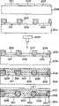
图1表示本发明有机EL元件的制造方法的第1实施例。该图也是表示3色的全色有机EL元件的制造方法的附图。该图中示出了一种有机EL元件的制造方法,该方法具有:在透明基板104上形成象素电极101、102、103的工序,在上述各象素电极上形成一种有机化合物构成的发光层106、107的图案形成工序,形成阴极113的工序,其特征在于,上述发光层的形成按照喷墨方式进行。FIG. 1 shows a first embodiment of the method for manufacturing an organic EL device of the present invention. This figure is also a drawing showing a method of manufacturing a three-color full-color organic EL element. This figure shows a method for manufacturing an organic EL element. The method includes the steps of forming
透明基板104作为支持体并同时具有作为光取出面的功能。因此,透明基板104可以根据透光性和热稳定性来选择。作为透明基板材料,例如可以举出玻璃基板、透明塑料板等,但从耐热性优良方面考虑,优选是玻璃基板。The
首先,在透明基板104上形成象素电极101、102、103。作为形成方法,例如可以举出光刻法、真空淀积法、溅射法、高温溶胶法等,其中优选是光刻法。作为象素电极,优选是透明象素电极,作为构成透明象素电极的材料,可以举出:氧化锡膜、ITO膜、氧化铟和氧化锌的复合氧化物膜等。First, the
然后是形成隔壁(挡板)105,用来填满上述各透明象素电极之间的间隙。Next, partition walls (blockers) 105 are formed to fill the gaps between the above-mentioned transparent pixel electrodes.
采用这种方法,可以提高对比度,防止发光材料的混色,防止象素与象素之间的漏光等。By adopting this method, the contrast ratio can be improved, the color mixing of the luminescent material can be prevented, the light leakage between pixels can be prevented, and the like.
作为构成隔壁105的材料没有特别限定,只要是对EL材料的溶剂具有耐久性的材料即可,例如可以举出:丙烯酸树脂、环氧树脂、感光性聚酰亚胺等的有机材料、液体玻璃等的无机材料等。另外,隔壁105也可以通过向上述材料中混入炭黑等来形成黑色挡光板。The material constituting the
作为该隔壁105的形成方法,例如可以举出光刻法等。As a method for forming the
进而,在各象素电极上按预定图案形成有机发光层,有机发光层优选是设置3色的发光层,优选是其中的至少1色按喷墨方式形成。Furthermore, an organic light-emitting layer is formed in a predetermined pattern on each pixel electrode, and the organic light-emitting layer is preferably provided with three-color light-emitting layers, preferably at least one of which is formed by inkjet.
按照图1的实施例,在象素电极101、102上分别按喷墨方式形成红色发光层106和绿色发光层107。According to the embodiment shown in FIG. 1, a red light-emitting
此处,所谓喷墨方式是指,由喷墨打印装置109的喷头110喷出一种由发光材料溶解或分散在溶剂中而形成的喷出液,从而形成在红色、绿色、蓝色这3种原色或其中间色中至少1种颜色的象素的过程而言。Here, the so-called inkjet method refers to that the
按照所说的喷墨方式,可以简便地而且在短时间内形成精细的图案。另外,通过增减喷出量来调整膜厚或者通过调整墨汁的浓度,即可以容易而且自由地控制发光的均衡性和亮度等的照明度。According to the ink-jet method, fine patterns can be formed easily and in a short time. In addition, by adjusting the film thickness by increasing or decreasing the discharge amount or by adjusting the concentration of ink, it is possible to easily and freely control the balance of light emission and illuminance such as brightness.
另外,当有机发光材料是下述的共轭高分子前体的情况下,可以在按喷墨方式喷出各种发光材料从而形成图案之后,通过加热或光照射等使上述前体成分共轭化(成膜)而形成发光层。In addition, when the organic luminescent material is a conjugated polymer precursor described below, after forming a pattern by ejecting various luminescent materials by an inkjet method, the above-mentioned precursor components can be conjugated by heating or light irradiation. Chemical (film formation) to form a light-emitting layer.
然后,如图1所示,在红色发光层106、绿色发光层107和象素电极103之上形成蓝色发光层108。按照该方法,不但可以形成红、绿、蓝的3原色,而且可以填平红色发光层106和绿色发光层107与隔壁105的垂直高差,从而使其平坦化。Then, as shown in FIG. 1 , a blue
作为形成上述蓝色发光层108的方法没有特殊限定,例如可以采用淀积法、湿法等一般成膜法,或者也可采用喷墨法来形成。The method for forming the blue light-emitting
另外,蓝色发光层108可以由例如象联苯乙烯衍生物那样的电子注入输送型材料构成。在此情况下促进了载流子的注入和输送,从而可以提高发光效率。进而,通过与由下述的空穴注入输送材料构成的薄层积叠在一起,可以使来自电极的电子和空穴平衡地注入并输送到发光层中,从而可以进一步地提高发光效率。In addition, the blue light-emitting
另外,在与空穴注入输送型材料等积叠的情况下,可以使空穴注入输送和电子注入输送分别由不同的材料来承担,因此可以分别对各种材料进行最适宜的设计。作为上述电子注入输送层的形成方法没有特殊限定,例如可以使用淀积法、湿法等一般的成膜法或者喷墨法。In addition, when stacked with a hole injection and transport type material, the hole injection and transport and the electron injection and transport can be performed by different materials, so that each material can be optimally designed. The method for forming the electron injecting and transporting layer is not particularly limited, and for example, a general film-forming method such as a deposition method or a wet method, or an inkjet method can be used.
另外,作为能够形成电子注入输送层的有机化合物,可以举出:PBD、OXD-8等噁二唑衍生物、DSA、羟基喹啉铝配合物、Bebq、三唑衍生物、甲亚胺配合物、卟吩配合物、苯并噁二唑配合物等,其中,可以用其中的1种或2种以上的混合物,或者通过积叠来形成电子注入输送层。另外,也可以在上述有机化合物中掺杂入下述的荧光色素来形成电子注入输送层。另外,上述电子注入输送层也可以具有发光的功能。In addition, examples of organic compounds capable of forming the electron injecting and transporting layer include oxadiazole derivatives such as PBD and OXD-8, DSA, quinoline aluminum complexes, Bebq, triazole derivatives, and imine complexes. , porphine complexes, benzoxadiazole complexes, etc. Among them, one type or a mixture of two or more types thereof can be used, or the electron injection and transport layer can be formed by stacking. In addition, the above-mentioned organic compound may be doped with a fluorescent dye described below to form an electron injecting and transporting layer. In addition, the electron injecting and transporting layer may have a function of emitting light.
按照本实施例,有机发光层中的2色按喷墨方式形成,另1色按其他方法形成,因此,即使是一种不太适合按喷墨方式形成的发光材料,也可以与某些适用于喷墨方式的其他有机发光材料组合来形成全色有机EL元件,因此可以加宽设计范围。According to this embodiment, two colors in the organic light-emitting layer are formed by inkjet, and the other color is formed by other methods. Therefore, even a light-emitting material that is not suitable for formation by inkjet can also be compatible with some suitable materials. In combination with other organic light-emitting materials in the inkjet method to form a full-color organic EL device, the design range can be broadened.
作为除了喷墨方式以外的发光层的形成方法,例如可以举出:光刻法、真空淀积法、印刷法、转印法、浸涂法、旋转涂布法、浇铸法、毛细管法、辊涂法、棒涂法等。As methods for forming the light-emitting layer other than the inkjet method, for example, photolithography, vacuum deposition, printing, transfer, dip coating, spin coating, casting, capillary, roll, etc. coating method, rod coating method, etc.
最后形成阴极(对置电极)113,从而制成本发明的有机EL元件。作为阴极113,优选是金属薄膜电极,作为构成阴极的金属,例如可以举出Mg、Ag、Al、Li等。另外,除了这些材料之外,一些功函数较小的材料也可以使用,例如可以使用碱金属或Ca等碱土类金属以及含有这些金属的合金。这样的阴极113可以用淀积法和溅射法等来形成。Finally, a cathode (counter electrode) 113 is formed, thereby producing the organic EL element of the present invention. The
本发明的有机EL元件可以通过上述的工序来制造。也就是说,如图1所示,在设置于透明基板104上的象素电极101和102之上,各自以喷墨方式按图案形成由有机化合物构成的红色发光层106、绿色发光层107,进而在上述发光层106、107和象素电极103之上以真空淀积法形成蓝色发光层108。最后在其上面形成阴极113,从而完成了本发明的有机EL元件。The organic EL element of the present invention can be produced through the above-mentioned steps. That is to say, as shown in FIG. 1, on the
然后,如图6所示,在阴极413之上形成保护膜415。由于形成了保护膜415,因此可以防止阴极413和各发光层406、407、408的劣化、损伤和剥离等。Then, as shown in FIG. 6 , a protective film 415 is formed over the cathode 413 . Since the protective film 415 is formed, deterioration, damage, peeling, and the like of the cathode 413 and the light emitting layers 406, 407, and 408 can be prevented.
作为上述保护膜415的构成材料,可以举出环氧树脂、丙烯酸树脂、液体玻璃等。另外,作为保护膜415的形成方法,例如可以举出:旋转涂布法、浇铸法、浸涂法、棒涂法、辊涂法、毛细管法等。Examples of the constituent material of the protective film 415 include epoxy resin, acrylic resin, liquid glass, and the like. In addition, examples of a method for forming the protective film 415 include spin coating, casting, dip coating, bar coating, roll coating, and capillary coating.
发光层优选由有机化合物构成,更优选由高分子有机化合物构成。通过形成由有机化合物构成的发光层,可以在低电压的条件下达到高亮度的表面发光。另外,由于发光材料可以在宽范围内选择,因此可以对EL发光元件进行合理的设计。The light-emitting layer is preferably composed of an organic compound, more preferably a polymeric organic compound. By forming a light-emitting layer made of an organic compound, high-brightness surface light emission can be achieved under low-voltage conditions. In addition, since luminescent materials can be selected in a wide range, rational design of EL light-emitting elements is possible.
特别是高分子有机化合物的成膜性优良,而且,由高分子有机化合物构成的发光层具有极良好的耐久性。另外,这些高分子有机化合物具有可见光区域的带隙和较高的导电性,其中,共轭系高分子的这种倾向特别显著。In particular, high-molecular organic compounds are excellent in film-forming properties, and the light-emitting layer composed of high-molecular organic compounds has extremely good durability. In addition, these high-molecular organic compounds have a band gap in the visible light region and high conductivity, and among them, such a tendency is particularly remarkable for conjugated polymers.
作为有机发光层材料,可以使用高分子有机化合物本身,或者使用可以通过加热而共轭化(成膜)的共轭高分子有机化合物的前体等。As the material for the organic light-emitting layer, a high-molecular organic compound itself, or a precursor of a conjugated high-molecular organic compound that can be conjugated (formed into a film) by heating, or the like can be used.
在使用共轭化(成膜)之前的前体作为发光材料的情况下,作为喷墨的喷出液,其粘度等容易调整,可以进行精密的图案成形,而且可以容易地控制发光层的发光特性和涂膜的性状。In the case of using a precursor before conjugation (film formation) as a light-emitting material, the viscosity, etc., of the inkjet discharge liquid can be easily adjusted, precise patterning can be performed, and the light emission of the light-emitting layer can be easily controlled. Properties and properties of coating films.
用于形成发光层的高分子有机化合物,优选是空穴注入输送型材料。这样可以促进载流子的注入和输送,从而提高发光效率。The high-molecular organic compound used to form the light-emitting layer is preferably a hole injection and transport type material. This can promote the injection and transport of carriers, thereby improving the luminous efficiency.
作为能够形成发光层的有机化合物,例如可以举出:PPV(聚(对亚苯亚乙烯))或其衍生物、PTV(聚(2,5-亚噻吩亚乙烯))等聚烷基亚噻吩、PFV(聚(2,5-亚呋喃亚乙烯))、聚对亚苯、聚烷基芴等聚亚芳基乙烯、吡唑啉二聚物、喹嗪(quinolidine)羧酸、高氯酸苯并吡喃鎓盐、苯并吡喃喹嗪、红荧烯、菲咯啉铕配合物等,可以使用其中的1种或2种以上的混合物。Examples of organic compounds capable of forming a light-emitting layer include polyalkylthiophenes such as PPV (poly(p-phenylene vinylene)) or derivatives thereof, and PTV (poly(2,5-thiophene vinylene)). , PFV (poly(2,5-furylidene vinylene)), polyparaphenylene, polyalkylfluorene and other polyarylene vinylene, pyrazoline dimer, quinolidine carboxylic acid, perchloric acid Benzopyrylium salts, benzopyranoquinazines, rubrene, phenanthroline europium complexes, and the like can be used alone or as a mixture of two or more of them.
其中优选是属于共轭高分子有机化合物的PPV或其衍生物。PPV或其衍生物共轭化(成膜)之前的前体可溶于水或有机溶剂中,因此适合于以喷墨方式进行图案形成。另外,由于是高分子,因此可以获得一种光学上高质量的并且其耐久性优良的薄膜。另外,PPV或其衍生物具有强的荧光,并且它是一种导电性的高分子,它的双键上的π电子是在聚合物链上的非定域化电子,因此PPV薄膜具有空穴注入输送层的功能,可以获得一种高性能的有机EL元件。Among them, PPV or its derivatives, which are conjugated polymeric organic compounds, are preferable. The precursor of PPV or its derivative before conjugation (film formation) is soluble in water or an organic solvent, and thus is suitable for pattern formation by an inkjet method. In addition, since it is a polymer, an optically high-quality thin film having excellent durability can be obtained. In addition, PPV or its derivatives have strong fluorescence, and it is a conductive polymer, and the π electrons on its double bond are delocalized electrons on the polymer chain, so the PPV film has holes By injecting the function of the transport layer, a high-performance organic EL element can be obtained.
另外,在使用高分子有机发光层材料的情况下,有机EL元件组合物也可以含有至少1种荧光色素。这样可以改变发光层的发光特性,例如可以有效地提高发光层的发光效率,或者作为改变光吸收极大波长(发光色)的有效手段。In addition, when a polymeric organic light-emitting layer material is used, the organic EL device composition may contain at least one fluorescent dye. In this way, the luminescent properties of the luminescent layer can be changed, for example, the luminous efficiency of the luminescent layer can be effectively improved, or it can be used as an effective means to change the maximum wavelength of light absorption (luminescent color).
也就是说,荧光色素不只是作为发光层材料使用,而且作为承担发光功能的色素材料使用。例如,通过PPV等那样的共轭系高分子有机化合物分子上的载流子再结合而生成的激子的能量,可以几乎完全地转移到荧光色素分子上。在此情况下,发出的光仅仅是由一种荧光量子效率高的荧光色素分子产生的,因此EL元件的电流量子效率也提高了。而且,通过向有机EL元件组合物中加入荧光色素,可以使得发光层发出的光谱同时成为荧光分子的光谱,因此可以有效地作为用于改变发光颜色的手段。That is to say, the fluorescent pigment is used not only as a light-emitting layer material, but also as a pigment material that undertakes a light-emitting function. For example, the energy of excitons generated by recombination of carriers on molecules of a conjugated polymer organic compound such as PPV can be almost completely transferred to fluorescent dye molecules. In this case, the emitted light is generated only by a fluorochrome molecule having a high fluorescence quantum efficiency, so the current quantum efficiency of the EL element is also improved. Furthermore, by adding a fluorescent dye to the organic EL device composition, the spectrum emitted from the light-emitting layer can simultaneously become the spectrum of fluorescent molecules, and thus can be effectively used as a means for changing the color of light emitted.
另外,此处所谓的电流量子效率是一个根据发光功能,用于考察发光性能的尺度,它可按下述公式来定义。In addition, the so-called current quantum efficiency here is a scale used to investigate the luminous performance according to the luminous function, and it can be defined according to the following formula.
ηε=放出的光子的能量/输入的电能ηε = energy of emitted photons / input electrical energy
于是,通过掺杂荧光色素来改变光吸收的极大波长,可以使其发出例如红、蓝、绿的3种原色的光,其结果是可以获得一种全色的显示装置。Therefore, by doping fluorescent dyes to change the maximum wavelength of light absorption, it is possible to emit light of three primary colors such as red, blue, and green. As a result, a full-color display device can be obtained.
另外,通过掺杂荧光色素,可以大幅度地提高EL元件的发光效率。In addition, the luminous efficiency of the EL element can be greatly improved by doping with a fluorescent dye.
作为适用于红色发光层中的荧光色素,可以使用属于激光色素的DCM或若丹明或若丹明的衍生物,以及苝等化合物。这些荧光色素是低分子量的,因此可溶于溶剂中,而且它们与PPV等的相溶性优良,而且容易形成一种均匀而且稳定的发光层。作为若丹明衍生物荧光色素,例如可以举出:若丹明B、若丹明B碱、若丹明6G、若丹明101高氯酸盐等,这些色素也可以是2种以上的混合物。As fluorescent dyes suitable for use in the red light-emitting layer, DCM, rhodamine or rhodamine derivatives, which are laser dyes, and compounds such as perylene can be used. These fluorochromes are low molecular weight and therefore soluble in solvents, and they are excellent in compatibility with PPV and the like, and easily form a uniform and stable light-emitting layer. Rhodamine derivative fluorescent dyes include, for example, rhodamine B, rhodamine B base, rhodamine 6G,
另外,作为适用于绿色发光层中的荧光色素,可以举出:喹吖酮、红荧烯、DCJT以及它们的衍生物。这些荧光色素与上述红色荧光色素同样地是低分子量的,因此可溶于溶剂中,另外,它们与PPV的相溶性良好,因此容易形成发光层。In addition, examples of fluorescent dyes suitable for use in the green light-emitting layer include quinacridone, rubrene, DCJT, and derivatives thereof. These fluorescent dyes are low molecular weight like the above-mentioned red fluorescent dyes, so they are soluble in solvents, and they have good compatibility with PPV, so it is easy to form a light-emitting layer.
作为适用于蓝色发光层的荧光色素,可以举出二苯乙烯基联苯及其衍生物。这些荧光色素也与上述红色荧光色素一样是在水溶液中可溶的,而且与PPV的相溶性良好,因此容易形成发光层。Distyryl biphenyl and its derivatives are mentioned as a fluorescent dye suitable for a blue light emitting layer. These fluorescent dyes are also soluble in aqueous solution like the above-mentioned red fluorescent dyes, and have good compatibility with PPV, so it is easy to form a light-emitting layer.
另外,其他作为适用于蓝色发光层中的荧光色素,可以举出:香豆素以及香豆素-1、香豆素-6、香豆素-7、香豆素120、香豆素138、香豆素152、香豆素153、香豆素311、香豆素314、香豆素334、香豆素337、香豆素343等的香豆素衍生物。In addition, other fluorescent dyes suitable for use in the blue light-emitting layer include coumarin, coumarin-1, coumarin-6, coumarin-7, coumarin-120, and coumarin-138 , coumarin 152, coumarin 153,
另外,其他作为适用于蓝色发光层中的发光材料,可以举出:四苯基丁二烯(TPB)或TPB衍生物、DPVBi等。这些发光材料也与上述的红色荧光色素等一样是低分子量的,因此可溶于溶剂中,而且,它们与PPV等的相溶性良好,因此容易形成发光层。In addition, other light-emitting materials suitable for use in the blue light-emitting layer include tetraphenylbutadiene (TPB) or TPB derivatives, DPVBi, and the like. These luminescent materials are also low molecular weight like the above-mentioned red fluorescent dyes, so they are soluble in solvents, and they have good compatibility with PPV and the like, so it is easy to form a luminescent layer.
以上的荧光色素和发光材料可以使用其中的1种或2种以上的混合物。One kind or a mixture of two or more kinds of the above fluorescent dyes and luminescent materials can be used.
在本发明的有机EL元件的制造方法中使用的喷墨用喷头的结构示于图10和图11中。The structure of the inkjet head used in the manufacturing method of the organic EL element of the present invention is shown in FIGS. 10 and 11 .
在该喷墨用喷头10具有例如不锈钢制的喷嘴板11和振动板13时,这两者通过隔离元件(储存板)15而接合起来。When the
在喷嘴板11与振动板13之间,由隔离元件15形成多个空间19和储液槽21。各空间19和储液槽21的内部充满本发明的组合物,各空间19与贮液槽21通过供给口23而相互连通。Between the nozzle plate 11 and the vibrating
另外,在喷嘴板11上设置一个用于将来自空间19的组合物以射流状喷出的喷嘴孔25。另一方面,在振动板13上形成一个用于将组合物供入储液槽21中的孔27。In addition, a
另外,与振动板13向着空间19的表面相对一侧的表面上,与上述空间19的位置相对应地粘接有压电元件29。In addition, a
该压电元件29处于一对电极31之间,一旦通入电流,压电元件29就向外侧突出挠曲,同时,与压电元件29接合在一起的振动板13也成为整体向外侧挠曲。如此就增大了空间19的容积。因此,与空间19内增大的那部分容积相当的组合物就通过供给口23由储液槽21流入空间19中。The
然后,一旦撤除通入压电元件29的电流,该压电元件29和振动板13就立即恢复其原来的状态。这时空间19也恢复至原来的容积,因此使得空间19内部的组合物的压力上升,从而导致组合物由喷嘴孔25向基板喷出。Then, when the current supplied to the
另外,在喷嘴孔25的周边部位设置有疏水层26,以便防止组合物的飞行途径弯曲和喷孔堵塞。In addition, a water-
也就是说,在喷嘴孔25的周边部位,如图11所示那样设置有例如由Ni-四氟乙烯共析的电镀层构成的疏水层26。That is, in the peripheral part of the
作用这样的喷头,通过按预定图案喷出与红、蓝、绿3原色相对应的组合物来形成各有机发光层,这样就形成了象素。Using such a nozzle, each organic light-emitting layer is formed by discharging compositions corresponding to the three primary colors of red, blue and green in a predetermined pattern, thus forming a pixel.
在本发明的有机EL元件的制造方法中,作为适用于喷墨方式的有机发光材料组合物,可以使用具有以下特性的组合物。In the method for producing an organic EL device of the present invention, a composition having the following characteristics can be used as the organic light-emitting material composition suitable for the inkjet method.
用于喷出上述组合物的喷嘴设置在喷墨用喷头上,因此,该组合物相对于构成上述喷嘴的喷嘴面251的材料的接触角优选为30°~170°,更优选为35°~65°。由于该组合物具有上述范围的接触角,因此可以抑制该组合物飞行途径的弯曲,从而能够形成精密的图案。The nozzles for ejecting the above-mentioned composition are arranged on an inkjet nozzle, and therefore, the contact angle of the composition with respect to the material of the
也就是说,当该接触角不足30℃时,组合物相对于喷嘴面构成材料的润湿性增大,因此在喷出该组合物时,该组合物有时会非对称地附着在喷嘴孔的周围。在此情况下,附着在喷嘴孔的组合物与被喷出的组合物相互之间存在引力作用,由于该组合物在喷出时受到不均匀的作用力,因此发生了不能达到目标位置的所谓飞行弯曲,并且飞行弯曲的频度也增高。另外,如果超过170°,则组合物与喷嘴孔之间的相互作用极小,在喷嘴先端处的弯月形状不稳定,因此对组合物喷出量和喷出定时的控制变得困难。That is, when the contact angle is less than 30° C., the wettability of the composition with respect to the constituent materials of the nozzle surface increases, so when the composition is ejected, the composition may asymmetrically adhere to the nozzle hole. around. In this case, there is an attractive force between the composition adhered to the nozzle hole and the ejected composition, and since the composition receives an uneven force when ejected, the so-called failure to reach the target position occurs. The flight bends, and the frequency of the flight bends increases. In addition, if it exceeds 170°, the interaction between the composition and the nozzle hole is extremely small, and the meniscus shape at the tip of the nozzle is unstable, so that it becomes difficult to control the ejection amount and ejection timing of the composition.
此处所谓飞行弯曲是指,组合物由上述喷嘴喷出时,组合物液滴的命中位置相对于目标位置发生50μm以上的偏移而言。另外,所谓飞行弯曲的频度是指组合物液滴开始以7200Hz的频率喷出时至发生上述飞行弯曲时的时间。飞行弯曲主要是由于喷嘴孔的润湿性不均匀或者由于组合物固体成分的附着而引起喷嘴孔堵塞等而发生的,这一现象可以通过清洗喷头的方法来消除。这种飞行弯曲的频度越高,就必须对喷头进行越频繁的清洗,因此这样一种会使飞行弯曲频度增高的组合物可以说是一种导致按喷墨方式的EL元件的制造效率降低的组合物。就实用水平而言,飞行弯曲的频度必须在1000秒以上。The flight deflection here means that when the composition is ejected from the nozzle, the impact position of the composition droplet deviates by 50 μm or more from the target position. In addition, the frequency of flight bending refers to the time from when the composition droplet starts to be ejected at a frequency of 7200 Hz to when the above-mentioned flight bending occurs. Flight bending is mainly caused by the uneven wettability of the nozzle hole or the clogging of the nozzle hole due to the adhesion of the solid component of the composition. This phenomenon can be eliminated by cleaning the nozzle. The higher the frequency of flight bending, the more frequently the nozzle must be cleaned, so such a composition that increases the frequency of flight bending can be said to be a method that leads to the manufacturing efficiency of EL elements by inkjet. Reduced composition. As far as the practical level is concerned, the frequency of flight bending must be above 1000 seconds.
由于可以防止这样的飞行弯曲,因此可以形成高精细的图案,并且可以高精度地进行。Since such flying bending can be prevented, it is possible to form a high-definition pattern with high precision.
另外,上述组合物的粘度优选为1cp~20cp,更优选为2cp~4cp。在组合物的粘度不足1cp时,上述前体和荧光色素在所说材料中的含量过小,从而使得形成的发光层不能充分地发挥发光能力。另一方面,在超过20cp时,组合物不能顺利地从喷嘴孔喷出,如果不采取扩大喷嘴孔径等变更装置规格的措施,则难以进行图案成形。另外,在粘度过大时,组合物中的固体成分容易析出,从而使得喷嘴孔被堵塞的发生频度增高。In addition, the viscosity of the composition is preferably 1 cp to 20 cp, more preferably 2 cp to 4 cp. When the viscosity of the composition is less than 1 cp, the content of the above-mentioned precursor and fluorescent pigment in the material is too small, so that the formed light-emitting layer cannot fully exhibit the light-emitting ability. On the other hand, when it exceeds 20 cp, the composition cannot be ejected smoothly from the nozzle hole, and it is difficult to perform pattern forming unless measures such as enlarging the diameter of the nozzle hole and changing the device specifications are taken. In addition, when the viscosity is too high, the solid content in the composition tends to precipitate, which increases the frequency of nozzle hole clogging.
另外,上述组合物的表面张力优选为20dyne/cm~70dyne/cm,更优选为25dyne/cm~40dyne/cm。通过使表面张力处于上述范围内,就能与上述接触角的情况一样地抑制飞行弯曲,并将飞行弯曲的频度抑制到较低程度。如果表面张力不足20dyne/cm,则组合物对喷嘴构成材料的润湿性增大,从而会与上述接触角的情况一样地产生飞行弯曲,并且使飞行弯曲的频度增高。另外,如果表面张力超过70dyne/cm,则在喷嘴先端处的弯月形状不稳定,因此对组合物喷出量和喷出定时的控制变得困难。In addition, the surface tension of the composition is preferably 20 dyne/cm to 70 dyne/cm, more preferably 25 dyne/cm to 40 dyne/cm. By setting the surface tension within the above range, flight bending can be suppressed similarly to the case of the above-mentioned contact angle, and the frequency of flight bending can be suppressed to a low level. If the surface tension is less than 20 dyne/cm, the wettability of the composition to the nozzle constituting material will increase, and flight bending will occur similarly to the case of the above-mentioned contact angle, and the frequency of flight bending will increase. In addition, if the surface tension exceeds 70 dyne/cm, the shape of the meniscus at the tip of the nozzle becomes unstable, so that control of the ejection amount and ejection timing of the composition becomes difficult.
另外,作为适用于本发明有机EL元件的制造方法的有机发光材料组合物,只要能够满足上述的接触角、粘度和表面张力中至少一个数值范围即可,优选是能够满足上述参数中2个以上任意组合的特性条件的组合物,更优选是能够满足所有特性的组合物。In addition, as the organic luminescent material composition suitable for the production method of the organic EL element of the present invention, as long as it can satisfy at least one numerical range among the above-mentioned contact angle, viscosity and surface tension, it is preferable that it can satisfy two or more of the above-mentioned parameters. The composition of any combination of characteristic conditions is more preferably a composition capable of satisfying all the characteristics.
图2示出本发明有机EL元件的制造方法的实施例2。FIG. 2 shows Embodiment 2 of the method for manufacturing an organic EL element of the present invention.
在本实施例中,与实施例1同样地在透明基材204上形成象素电极201、202、203和隔壁205,然后按喷墨方式形成红色发光层206、绿色发光层207。In this embodiment,
与上述实施例1不同之处在于,在象素电极203上形成空穴注入输送层208,然后再在该层上面积叠蓝色发光层210。通过如此积叠空穴注入输送层208,促进了如上所述来自电极的空穴的注入和输送,从而可以提高发光效率。The difference from the first embodiment above is that a hole injection and
这样,在本发明的有机EL元件的制造方法中,优选是将至少1色的发光层与空穴注入输送层积叠起来。如此就能提高发光效率,并且可以进一步提高薄膜元件本身的稳定性。Thus, in the method of manufacturing the organic EL device of the present invention, it is preferable to stack at least one color light-emitting layer and the hole injection and transport layer. In this way, the luminous efficiency can be improved, and the stability of the thin film element itself can be further improved.
另外,在积叠的发光层与空穴注入输送层的界面附近,两层中各自所含材料的一部分也可以存在相互向他层一侧渗透和扩散的状态。In addition, in the vicinity of the interface between the stacked light-emitting layer and the hole injection and transport layer, a part of the materials contained in each of the two layers may permeate and diffuse toward the other layer side.
空穴注入输送层208优选是不发光的层。这样就能使蓝色发光层210在象素电极203之上成为发光部,从而能够比较容易地制得全色的有机EL元件。The hole injection and
上述空穴注入输送层208的形成方法没有特别限定,例如可以按喷墨方式来形成。这样就可以按照精度优良的预定图案来配置该空穴注入输送层208。The method for forming the above-mentioned hole injection and
作为空穴输送层208的构成材料,例如可以举出:TPD等的芳香族二胺类化合物、MTDATA、喹吖酮、bisstil蒽衍生物、PVK(聚乙烯咔唑)、酞菁铜等酞菁类配合物、卟吩类化合物、NPD、TAD、聚苯胺等,其中优选为PVK。通过使用PVK,可以形成不发光的空穴注入输送层。Examples of the constituent material of the
进而,与上述实施例1同样地形成蓝色发光层210和阴极211,这样即可以获得本发明的有机EL元件。蓝色发光层210、阴极211的构成材料和形成方法与上述实施例相同。Furthermore, the organic EL element of the present invention can be obtained by forming the blue
图3示出本发明有机EL元件制造方法的实施例3。Fig. 3 shows Embodiment 3 of the method for manufacturing an organic EL element of the present invention.
在本实施例中,与实施例1同样地在透明基材304上设置象素电极301、302、303和隔壁305,然后按喷墨方式设置红色发光层306和绿色发光层307 。In this embodiment,
然后在红色发光层306、绿色发光层307和象素电极303上方的全部面积上形成空穴注入输送层308。如上所述,通过将空穴注入输送层308与发光层306和307积叠起来,可以促进空穴的注入和输送,从而能够提高发光效率。Then, the hole injecting and transporting
另外,根据与上述相同的理由,作为空穴注入输送层308,优选设置不发光的层。In addition, for the same reason as above, it is preferable to provide a layer that does not emit light as the hole injecting and transporting
对上述空穴注入输送层308的形成方法没有特别限定,例如可以举出:喷墨方式、真空淀积法、浸涂法、旋转涂布法、浇铸法、毛细管法、辊涂法、棒涂法等。在本实施例中可以通过真空淀积法来形成。另外,作为空穴注入输送层的构成材料,可以使用与上述实施例2相同的材料。The method for forming the above-mentioned hole injecting and transporting
然后在空穴注入输送层308之上形成蓝色发光层309和阴极311,这样即能获得本发明的有机EL元件。阴极311的构成材料和形成方法与上述实施例相同。Then, a blue light-emitting
图4示出本发明有机EL元件制造方法的实施例4。Fig. 4 shows Embodiment 4 of the method for manufacturing an organic EL element of the present invention.
在本实施例中,与实施例1同样地在透明基材804之上形成象素电极801、802、803和隔壁805,然后在象素电极801、802、803之上各自以喷墨方式按图案形成发光层806、806和808。这样就可以容易而且简便地对例如各发光层材料的喷出量、喷出次数和形成图案进行调节,并且能容易地对各发光层的发光特性、膜厚等膜的性状进行控制。In this embodiment,
然后在各发光层806、807、808之上形成电子注入输送层811。电子注入输送层811可以使来自阴极的电子容易地注入,另外,由于发光部分远离阴极,因此可以防止电极消光,并能与阴极形成较好的接触。作为电子注入输送层811,可以使用未经掺杂的羟基喹啉铝配合物。上述的电子注入输送层811可以通过真空淀积法来形成。An electron injection and
另外,对电子注入输送层811的形成方法没有限定,例如它可以是喷墨法、真空淀积法、浸涂法、旋转涂布法、浇铸法、毛细管法、辊涂法、棒涂法等。In addition, the method of forming the electron injection and
进而在其上面形成阴极813,从而获得了本发明的有机EL元件。阴极813的构成材料和形成方法与上述实施例相同。Further, a
图5示出本发明有机E L元件制造方法的实施例5。Fig. 5 shows Embodiment 5 of the manufacturing method of the organic EL element of the present invention.
在本实施例中,首先与实施例1同样地在透明基材804上设置象素电极801、802和803。再在其上方的全部面积上用旋转涂敷法形成一层例如由PVK构成的空穴注入输送层815。这样不需经过图案成形就能全部涂敷空穴注入输送层815并使其成膜,因此可以提高制造效率。In this embodiment,
另外,对空穴注入输送层815的形成方法没有限定,例如它可以是喷墨法、真空淀积法、浸涂法、旋转涂布法、浇铸法、毛细管法、辊涂法、棒涂法等。In addition, the method of forming the hole
另外,根据与上述同样的理由,空穴注入输送层815优选是不发光的层。In addition, for the same reason as above, the hole injection and
然后在空穴注入输送层815之上形成发光层806、807和808。其中至少有1色的发光层优选使用喷墨印刷装置809,按照喷墨法来形成图案。
进而在发光层上形.成阴极813,从而获得了本发明的有机EL元件。阴极813的构成材料和形成方法与上述实施例相同。And then in the shape of the light-emitting layer. into a
另外,在本实施例的制造方法中不设置隔壁,但是只要按照本发明的有机EL元件的制造方法,就可以高精度地分别进行R、G、B的涂敷,从而可以提高制造效率。但是也可以与上述实施例同样地设置隔壁以分别形成各象素。In addition, in the manufacturing method of this embodiment, partition walls are not provided, but according to the manufacturing method of the organic EL element of the present invention, R, G, and B can be applied separately with high precision, thereby improving manufacturing efficiency. However, it is also possible to provide partition walls to form individual pixels in the same manner as in the above-mentioned embodiments.
本发明的有机EL元件虽然可以按如上所述的方法来制造,但是并不限定于这些方法,例如它也可以具有如下构成。Although the organic EL element of the present invention can be produced by the methods described above, it is not limited to these methods, and it may have the following configuration, for example.
图15是表示本发明的有机EL元件另一个实例的部分截面图。Fig. 15 is a partial sectional view showing another example of the organic EL element of the present invention.
本实施例的有机EL元件是在透明基板61上顺次地积叠反射层62、透明导电性膜(ITO膜)63、空穴注入输送层64、有机发光层65、金属层66、透明导电性膜(ITO膜)67而构成。下面对各层的材料和形成方法进行说明,但是与上述各实施例相同的事项则省略其说明,仅仅说明它们的不同之处。In the organic EL element of this embodiment, a
本实施例的有机EL元件直接地在透明基板61上设置一层由Al等的金属薄膜构成的反射层62。In the organic EL element of this embodiment, a
另外,作为阴极而积叠在发光层65之上的金属层66十分薄(10~
由于具有这样的构成,所以由电极注入的电流在发光层65中转换成的光就按照图中箭头所示的方向透过。因此,不需通过透明基板61就可以将光取出,从而可以获得更高亮度的显示。With such a configuration, the light converted into the light-emitting
图7表示本发明的有机EL显示装置的一个实例。FIG. 7 shows an example of the organic EL display device of the present invention.
在本实施例中,在玻璃板501上通过光刻成象法形成一种Al制的总线(栅极线)511,然后在其上面形成图中没有示出的薄膜晶体管,进而形成504等的ITO透明象素电极。然后与实施例1同样地按喷墨方式形成发光层502(红)、503(绿),进而按真空淀积法形成蓝色发光层505。然后用真空淀积法形成阴极506,这样就制成了与上述实施例1同样的有机EL元件。In this embodiment, a bus (gate line) 511 made of Al is formed on the
之后将保护基材507通过周边密封件509而固定地贴合在透明基板501上。Afterwards, the
然后,将该显示装置放在氩气等惰性气体的气氛中,通过封孔513导入惰性气体512,最后用封孔材料508将封孔513密封。由于密封入惰性气体512,因此可以防止有机EL元件受到水分等来自外部的污染物和环境变化的影响,从而能够保持有机EL显示装置的发光性能。封孔材料508优选由不能透过惰性气体512的材料构成。Then, put the display device in an atmosphere of an inert gas such as argon, introduce an
银胶510具有能使阴极506与栅极线511在所说元件上实现接触的功能。The
栅极线511是薄膜晶体管(TFT)的开-关执行单元,起一种控制的作用,该TFT设置在每一个显示象素上,以便对显示象素作出选择。在写入时,使一行栅极线511的电位成为选择的水平,从而使该行的TFT成为导通状态。这时,只要由各列电源电极配线(图中未示出)向对应的象素供给图象信号电压,该图象信号电压就会通过TFT到达象素电极,于是向象素充电或使贮存在象素内的电荷放电,直至达到该信号电压的水平为止。The
图8示出使用本发明有机EL元件的有源矩阵型有机EL显示装置的一个实例。该实施例的有机EL显示装置按矩阵形配置,而且各自具有由R、G、B的发光部形成的许多发光象素构成的图象显示配置。FIG. 8 shows an example of an active matrix type organic EL display device using the organic EL element of the present invention. The organic EL display device of this embodiment is arranged in a matrix, and each has an image display arrangement composed of a plurality of light-emitting pixels formed of R, G, and B light-emitting portions.
如该图所示,在基板(图中未示出)上形成许多按相互正交排列的信号线(信号电极)601和栅极线(栅极)602,在每一象素中皆具有与信号线601和栅极线602相连接的薄膜晶体管(TFT)604,该TFT604与连接在其上面的由有机EL元件形成的发光层605、606积叠在一起。另外,在有机发光层中,至少有1色的发光层按喷墨方式形成。As shown in the figure, a plurality of signal lines (signal electrodes) 601 and gate lines (gates) 602 arranged orthogonally to each other are formed on a substrate (not shown in the figure), and each pixel has a A thin film transistor (TFT) 604 connected to the
图9是表示本发明有源矩阵型有机EL显示装置的截面图。Fig. 9 is a cross-sectional view showing an active matrix type organic EL display device of the present invention.
首先在透明基板904上形成预定的薄膜晶体管915和图中没有示出的栅极线、信号线等。然后在具有该薄膜晶体管915等预定功能元件的各象素电极(ITO)901、902、903之上形成覆盖着每一个象素电极的空穴注入输送层911。作为空穴注入输送型材料,可以使用与上述实施例同样的物质。另外,空穴注入输送层911的形成方法没有特别限定,它可以按上述任一种方法形成。Firstly, predetermined
进而按图案形成各发光层906(红)、907(绿)、908(蓝)。发光层的形成,可以使用喷墨打印装置910按照喷墨方式来形成其中至少1色的发光层。Furthermore, respective light emitting layers 906 (red), 907 (green), and 908 (blue) are formed in a pattern. For the formation of the luminescent layer, the luminescent layer of at least one color can be formed by using the
最后形成反射电极913,从而制得本发明的有机EL显示装置。作为反射电极913,例如可以形成一种厚度为0.1~0.2μm左右的Mg-Ag电极等。Finally, the
在本发明的有源矩阵型有机EL显示装置的上述实施例中,虽然是使用薄膜晶体管作为开关元件,但对此没有限定,也可以使用其他种类的开关元件、二极管,例如MIM等开关元件。另外也可以采用无源驱动、静态驱动(静止图象、局部显示)等。In the above-mentioned embodiments of the active matrix organic EL display device of the present invention, although thin film transistors are used as switching elements, there is no limitation to this, and other types of switching elements, diodes, such as MIM and other switching elements can also be used. In addition, passive driving, static driving (still image, partial display) and the like can also be used.
另外,一个象素不限于只用一个开关元件,对于一个象素可以配备多个开关元件。In addition, one pixel is not limited to only one switching element, and a plurality of switching elements may be provided for one pixel.
图12示出对于一个象素配备有多个开关元件的有机EL显示装置的实例。在此情况下,开关薄膜晶体管142根据扫描电极131的电位,将信号电极132的电位传达给电流薄膜晶体管143,该电流薄膜晶体管143对于公共电极133和象素电极141的导通起一种控制作用。Fig. 12 shows an example of an organic EL display device equipped with a plurality of switching elements for one pixel. In this case, the switching
下面根据附图解释使用本发明有机EL元件的无源矩阵(单纯矩阵)型有机EL显示装置的一个实例。An example of a passive matrix (simple matrix) type organic EL display device using the organic EL element of the present invention is explained below with reference to the drawings.
图13是本发明的有机EL显示装置的概略部分放大截面图。13 is a schematic partial enlarged cross-sectional view of the organic EL display device of the present invention.
如图所示,在本实施例的有机EL显示装置中,在制造有机EL元件时,薄长方形的扫描电极53和信号电极54通过有机EL元件52而相互正交配置。As shown in the figure, in the organic EL display device of this embodiment, when the organic EL element is manufactured, the thin
这样的无源矩阵型的驱动可按下述方式进行,也就是以脉冲方式顺次地选择扫描电极53,在选择该扫描电极53时,同时选择与各象素相对应的信号电极54并向其施加电压。这样的选择可以由控制器55来控制。The driving of such passive matrix type can be carried out in the following manner, that is, the
应予说明,在无源驱动型的情况下,阴极(cathode)必须形成图案,以便将各条线分隔开。例如,在本发明的第3实施例中,在形成厚度为0.2μm左右的薄阴极时,该阴极被隔壁分隔开,这样就自然地成为已形成图案的状态。It should be noted that in the case of the passive driving type, the cathode must be patterned so as to separate the lines. For example, in the third embodiment of the present invention, when a thin cathode having a thickness of about 0.2 μm is formed, the cathode is partitioned by barrier ribs, and thus is naturally patterned.
阴极可以按照例如掩模淀积法、激光切割法来进行图案形成。The cathode can be patterned by, for example, mask deposition or laser cutting.
图14中示出了向扫描电极13和信号电极14施加电压的电压驱动波形的一个实例。在该图所示的驱动波形中,向选择出的象素施加足以使其发光的电压Vs。另外,根据与浓淡度相符合的脉冲幅度波形,可以控制象素的显示浓度。另一方面,对于未被选择的象素则施加在发光阈值电压以下的电压Vn。An example of voltage drive waveforms for applying voltages to scan
在图14中,Tf表示操作时间。在此情况下,按占空比为1/100进行驱动。另外,由上述实施例4的有机EL元件构成的有机EL显示装置的蓝色发光层808所发出的光,当驱动电压为20V时,其亮度为100cd/m2。In FIG. 14, Tf represents the operation time. In this case, driving is performed with a duty ratio of 1/100. In addition, the light emitted from the blue
(实施例)(Example)
[有机EL元件的制造][Manufacture of organic EL elements]
(实施例1)(Example 1)
如图1所示,在玻璃基板104上按光刻法形成ITO透明象素电极101、102和103,从而形成100μm间距和0.1μm厚的图案。As shown in FIG. 1, ITO
然后掩埋ITO透明象素电极之间的空隙,再用光刻法形成一种兼有遮光和防止墨水流失两种作用的隔壁105。该隔壁105的宽为20μm,厚为2.0μm。Then bury the gaps between the ITO transparent pixel electrodes, and then use photolithography to form a
进而,利用喷墨印刷装置109的喷头110喷出表1和表2中示出的红色、绿色的各种发光材料以形成图案,然后在氮气气氛中于150℃的温度下加热处理4小时,借此使组合物中的前体聚合成高分子,从而形成各发光层106(红)和107(绿)。Furthermore, various red and green light-emitting materials shown in Table 1 and Table 2 were ejected by the
然后利用一种添加有苝的缩合芳香族化合物作为掺杂剂的羟基喹啉铝进行真空淀积,借此形成一层0.1μm的电子注入输送层型的蓝色发光层108。Vacuum deposition was then performed using aluminum quinoline added with a condensed aromatic compound of perylene as a dopant, whereby a blue light-emitting
最后用淀积法形成一层厚度为0.8μm的Mg-Ag电极113作为阴极,从而制成了有机EL元件。Finally, a layer of Mg-
(实施例2)(Example 2)
与实施例1同样,按图2所示在玻璃基板204上形成ITO透明象素电极201、202和203,然后掩埋ITO透明象素电极之间的空隙,进而形成兼有遮光和防止墨水流失两种作用的感光性聚酰亚胺的阻挡墙(隔壁)205。Same as Embodiment 1, form ITO
进而与实施例1同样地使用一台喷墨印刷装置209,按图案涂敷表1和表2中所示的红色、绿色的各种发光材料,然后在氮气气氛中和150℃的温度下加热处理4小时,借此使组合物中的前体聚合成高分子,从而形成各发光层206(红)和207(绿)。Furthermore, using an
然后使用上述的喷墨印刷装置209,在透明象素电极203上按图案形成一层由聚乙烯咔唑(PVK)构成的空穴注入输送层。接着在其上面涂敷一层吡唑啉二聚物,从而形成了蓝色发光层210。Then, a hole injecting and transporting layer made of polyvinylcarbazole (PVK) was formed on the
最后用淀积法形成一层厚度为0.8μm的Al-Li电极211作为阴极,从而制成了有机EL元件。Finally, an Al-Li electrode 211 with a thickness of 0.8 μm was formed as a cathode by a deposition method, thereby making an organic EL element.
(实施例3)(Example 3)
首先与实施例1同样,按图4所示在玻璃基板804上形成ITO透明象素电极801、802、803和隔壁805。First, ITO
然后向表1和表2所示的发光材料中混入有机空穴注入输送型材料,使用一台喷墨打印装置809形成各发光层806(红)、807(绿)和808(蓝)。Then, an organic hole injection transport type material was mixed into the light emitting materials shown in Table 1 and Table 2, and each light emitting layer 806 (red), 807 (green) and 808 (blue) was formed using an
然后使用一种未经掺杂的羟基喹啉铝配合物进行真空淀积,形成了一层厚度为0.1μm的电子注入输送层811。Then vacuum deposition was performed using an undoped quinoline aluminum complex to form an electron injection and
最后用淀积法形成一层厚度为0.2μm的AL-Li电极813,从而制成了有机EL元件。Finally, an AL-
(实施例4)(Example 4)
与实施例1同样,按图3所示在玻璃基板304上形成各个ITO透明象素电极301、302、303和隔壁305。In the same manner as in Embodiment 1, individual ITO
然后与实施例1同样地使用一台喷墨印刷装置310,按图案涂敷表1和表2中所示的红色、绿色的各种发光材料,然后在氮气气氛中和150℃的温度下加热处理4小时,借此使组合物中的前体聚合成高分子,从而形成各发光层306(红)和307(绿)。Then use an
然后在发光层306、307和透明象素电极303之上的全部面积上用涂敷法形成一层由聚乙烯咔唑(PVK)构成的空穴注入输送层308 。Then, on the entire area above the light-emitting
接着在空穴注入输送层308上用真空淀积法形成一层由联苯乙烯衍生物构成的蓝色发光层309。Next, a blue light-emitting
最后用淀积法形成一层厚度为0.8μm的Al-Li电极311作为阴极,从而制成了有机EL元件。这时,如上所述,阴极311被隔壁305自然地分隔开并被其绝缘,从而使各象素电极301、302、303共同构成图案状态。Finally, an Al-
(实施例5)(Example 5)
首先与实施例1同样,按图4所示在玻璃基板804上形成ITO透明象素电极801、802、803和隔壁805。First, ITO
进而使用一台喷墨印刷装置809喷出表1和表2中所示的高分子有机发光材料,按图案涂敷各色发光材料,然后在氮气气氛中和150℃的温度下加热处理4小时,借此使组合物中的前体聚合成高分子,从而形成能发出红色、绿色和蓝色的各发光层806(红)、807(绿)和808(蓝)。Furthermore, an
然后使用一种未经掺杂的羟基喹啉铝配合物进行真空淀积,形成了一层厚度为0.1μm的电子注入输送层811。Then vacuum deposition was performed using an undoped quinoline aluminum complex to form an electron injection and
最后用淀积法形成一层厚度为0.8μm的Al-Li电极813作为阴极,从而制成了有机EL元件。Finally, an Al-
2.对发光层的发光性能和膜性能的评价2. Evaluation of the luminescent properties and film properties of the luminescent layer
对于在上述实施例1~5中制得的有机EL元件的发光层的发光性能和膜性能按下述方法进行评价。The light-emitting properties and film properties of the light-emitting layers of the organic EL elements prepared in Examples 1 to 5 above were evaluated by the following methods.
①发光开始电压①Emission start voltage
向元件施加预定的电压,把观测到1cd/m2的发光亮度时的施加电压定义为发光开始电压[Vth]。A predetermined voltage was applied to the element, and the applied voltage at which a luminance of 1 cd/m2 was observed was defined as the luminescence start voltage [Vth].
②发光寿命②Luminescence life
以稳定化处理后的初期亮度作为100%,按标准波形施加一定的电流使其连续发光,测定其亮度的变化,以其亮度开始低于初期亮度的50%时的时间定义为发光寿命。Taking the initial luminance after stabilization treatment as 100%, apply a certain current according to the standard waveform to make it emit light continuously, measure the change of luminance, and define the luminescence life as the time when the luminance starts to be lower than 50% of the initial luminance.
应予说明,驱动条件是:室温:40℃;湿度:23%;电流值:20mA/cm2。It should be noted that the driving conditions are: room temperature: 40°C; humidity: 23%; current value: 20 mA/cm2 .
③发光亮度③ Luminous brightness
在电流值为20mA/cm2时测得的亮度。Brightness measured at a current value of 20mA/cm2 .
④吸收极大波长④ Absorb maximum wavelength
测定各发光层的吸收极大波长。The absorption maximum wavelength of each light-emitting layer was measured.
⑤成膜稳定性⑤ Film Stability
将发光层在200℃下加热60分钟之后,用显微镜观察发光层的裂纹或变形等缺陷发生的情况。After heating the light-emitting layer at 200° C. for 60 minutes, occurrence of defects such as cracks and deformations in the light-emitting layer was observed with a microscope.
评价按照如下方式进行。Evaluation was performed as follows.
◎…非常良好◎…very good
○…良好○...good
×…不良×… Bad
所获结果示于表3和表4中。The results obtained are shown in Table 3 and Table 4.
如表3和表4所示,在实施例1~5的任一个实施例中,各发光层的发光性能和发光层的膜性能均优良。特别是在发光层由高分子有机化合物构成的情况下,在各发光层中完全观察不到缺陷,这说明形成了非常良好的薄膜。As shown in Table 3 and Table 4, in any of Examples 1 to 5, the light-emitting performance of each light-emitting layer and the film performance of the light-emitting layer were excellent. In particular, when the light-emitting layer was made of a high-molecular organic compound, no defect was observed in each light-emitting layer, which indicates that a very good thin film was formed.
以上根据图示的各实施例解释了本发明的有机EL元件用组合物和有机EL元件的制造方法,但本发明不受这些实施例的限定,例如,也可以安排在各层之间形成任意功能性中间层的工序。另外,对于为了改变发光性能而添加的荧光色素也没有限制。The composition for organic EL elements of the present invention and the manufacturing method of organic EL elements have been explained above according to the illustrated embodiments, but the present invention is not limited by these embodiments, for example, it can also be arranged to form any The process of the functional middle layer. In addition, there is no limitation on the fluorochromes added to change the luminescent properties.
另外,也可以在各层之间形成一层例如由1,2,4-三唑衍生物(TAZ)构成的层作为缓冲层,这样可以进一步地提高发光亮度和发光寿命等。In addition, a layer composed of, for example, 1,2,4-triazole derivatives (TAZ) may be formed between each layer as a buffer layer, so that the luminous brightness and luminous lifetime can be further improved.
另外,在本发明的有机EL元件的制造方法中,为了使EL材料易于粘附,可以具有对树脂保护膜、象素电极和底层的表面进行等离子体处理、UV处理、偶合等表面处理的工序。另外,本发明的有机EL元件的制造方法也可以应用于无机EL元件的制造方法中。In addition, in the manufacturing method of the organic EL element of the present invention, in order to make the EL material easy to adhere, it may have a process of performing surface treatment such as plasma treatment, UV treatment, coupling, etc. on the surface of the resin protective film, the pixel electrode and the bottom layer. . In addition, the method for manufacturing an organic EL element of the present invention can also be applied to a method for manufacturing an inorganic EL element.
另外,本发明的有机EL显示装置可以应用于局部显示或全面同时发光的静止图象显示,例如图画、文字、名牌等低信息量的领域,或者,也可作为具有点、线、面形状的光源使用。In addition, the organic EL display device of the present invention can be applied to partial display or full-scale simultaneous light-emitting still image display, such as low-information fields such as pictures, characters, and nameplates, or it can also be used as a display with point, line, and surface shapes. light source used.
如上所述,按照本发明有机EL元件的制造方法,通过在较宽范围内选择发光材料,可以对EL发光元件进行合理的设计。例如,通过将发光材料与荧光色素进行组合等,可以获得各种显示光。As described above, according to the manufacturing method of the organic EL element of the present invention, the EL light emitting element can be rationally designed by selecting the light emitting material in a wide range. For example, various display lights can be obtained by combining a luminescent material with a fluorescent dye or the like.
另外,通过使用有机发光材料,可以展开有关高亮度和长寿命的各种各样的EL元件的设计。In addition, the use of organic light-emitting materials enables the design of various EL elements related to high brightness and long life.
另外,通过按喷墨方式依照图案形成和排列至少1色的有机发光层、空穴注入输送层和电子注入输送层,可以任意而且精密地设定发光元件的大小或图案。In addition, by forming and arranging at least one color organic light-emitting layer, hole injection and transport layer, and electron injection and transport layer according to a pattern in an inkjet method, the size and pattern of the light-emitting element can be set arbitrarily and precisely.
在使用一种能够通过加热固化来使其共轭化(成膜)的前体作为发光材料的情况下,可以使粘度等条件设定的自由度增大,能够容易地调整适合作为喷墨用喷出液的条件。In the case of using a precursor that can be conjugated (film-formed) by heating and curing as a light-emitting material, the degree of freedom in setting conditions such as viscosity can be increased, and it can be easily adjusted to be suitable for inkjet use. The condition of the ejected liquid.
另外,按照本发明的有机EL元件的制造方法,可以任意地调整膜厚、点数等条件,因此可以容易地控制发光层的发光性能。In addition, according to the manufacturing method of the organic EL device of the present invention, conditions such as the film thickness and the number of dots can be adjusted arbitrarily, so the light-emitting performance of the light-emitting layer can be easily controlled.
另外,按照喷墨方式,可以使喷头在透明基板上自由地移动,因此,对基板的大小没有限制,可以形成任意大小的元件。另外,由于可以将只限于必要量的材料配置在指定的部位,因此可以最大程度地避免产生废液等的废物。从而可以廉价地制造大画面的全色显示装置。In addition, according to the inkjet method, the nozzle can move freely on the transparent substrate, so there is no limit to the size of the substrate, and components of any size can be formed. In addition, since only the necessary amount of material can be placed in a designated location, waste such as waste liquid can be avoided to the greatest extent. Therefore, a large-screen full-color display device can be manufactured at low cost.

Claims (23)
Translated fromChineseApplications Claiming Priority (3)
| Application Number | Priority Date | Filing Date | Title |
|---|---|---|---|
| JP31382896AJP3899566B2 (en) | 1996-11-25 | 1996-11-25 | Manufacturing method of organic EL display device |
| JP313828/1996 | 1996-11-25 | ||
| JP313828/96 | 1996-11-25 |
Related Parent Applications (1)
| Application Number | Title | Priority Date | Filing Date |
|---|---|---|---|
| CNB971925461ADivisionCN1138458C (en) | 1996-11-25 | 1997-11-25 | Organic electroluminescent element, method for manufacturing the same, and organic electroluminescent display device |
Related Child Applications (3)
| Application Number | Title | Priority Date | Filing Date |
|---|---|---|---|
| CN2006101016623ADivisionCN1953239B (en) | 1996-11-25 | 1997-11-25 | Method of manufacturing organic el element, organic el element, and organic el display device |
| CNB200610101652XADivisionCN100477251C (en) | 1996-11-25 | 1997-11-25 | Manufacturing method of organic electroluminescence element |
| CNA2006101016534ADivisionCN1905157A (en) | 1996-11-25 | 1997-11-25 | Organic EL element and method of manufacturing organic EL element, and organic EL display device |
Publications (2)
| Publication Number | Publication Date |
|---|---|
| CN1523938A CN1523938A (en) | 2004-08-25 |
| CN100392891Ctrue CN100392891C (en) | 2008-06-04 |
Family
ID=18046006
Family Applications (5)
| Application Number | Title | Priority Date | Filing Date |
|---|---|---|---|
| CNA2006101016534APendingCN1905157A (en) | 1996-11-25 | 1997-11-25 | Organic EL element and method of manufacturing organic EL element, and organic EL display device |
| CNB2003101102998AExpired - LifetimeCN100392891C (en) | 1996-11-25 | 1997-11-25 | Organic electroluminescent element, method for manufacturing the same, and organic electroluminescent display device |
| CNB971925461AExpired - LifetimeCN1138458C (en) | 1996-11-25 | 1997-11-25 | Organic electroluminescent element, method for manufacturing the same, and organic electroluminescent display device |
| CNB200610101652XAExpired - LifetimeCN100477251C (en) | 1996-11-25 | 1997-11-25 | Manufacturing method of organic electroluminescence element |
| CN2006101016623AExpired - LifetimeCN1953239B (en) | 1996-11-25 | 1997-11-25 | Method of manufacturing organic el element, organic el element, and organic el display device |
Family Applications Before (1)
| Application Number | Title | Priority Date | Filing Date |
|---|---|---|---|
| CNA2006101016534APendingCN1905157A (en) | 1996-11-25 | 1997-11-25 | Organic EL element and method of manufacturing organic EL element, and organic EL display device |
Family Applications After (3)
| Application Number | Title | Priority Date | Filing Date |
|---|---|---|---|
| CNB971925461AExpired - LifetimeCN1138458C (en) | 1996-11-25 | 1997-11-25 | Organic electroluminescent element, method for manufacturing the same, and organic electroluminescent display device |
| CNB200610101652XAExpired - LifetimeCN100477251C (en) | 1996-11-25 | 1997-11-25 | Manufacturing method of organic electroluminescence element |
| CN2006101016623AExpired - LifetimeCN1953239B (en) | 1996-11-25 | 1997-11-25 | Method of manufacturing organic el element, organic el element, and organic el display device |
Country Status (8)
| Country | Link |
|---|---|
| US (7) | US6863961B2 (en) |
| EP (4) | EP1211916B1 (en) |
| JP (1) | JP3899566B2 (en) |
| KR (4) | KR100493131B1 (en) |
| CN (5) | CN1905157A (en) |
| DE (2) | DE69727212T2 (en) |
| TW (1) | TW553579U (en) |
| WO (1) | WO1998024271A1 (en) |
Families Citing this family (493)
| Publication number | Priority date | Publication date | Assignee | Title |
|---|---|---|---|---|
| KR100479000B1 (en)* | 1996-05-15 | 2005-08-01 | 세이코 엡슨 가부시키가이샤 | Manufacturing method of thin film device, liquid crystal panel and electronic device and thin film device |
| JP3899566B2 (en)* | 1996-11-25 | 2007-03-28 | セイコーエプソン株式会社 | Manufacturing method of organic EL display device |
| US6462722B1 (en) | 1997-02-17 | 2002-10-08 | Seiko Epson Corporation | Current-driven light-emitting display apparatus and method of producing the same |
| CN100341042C (en) | 1997-02-17 | 2007-10-03 | 精工爱普生株式会社 | Display device |
| JP3541625B2 (en)* | 1997-07-02 | 2004-07-14 | セイコーエプソン株式会社 | Display device and active matrix substrate |
| JP3520396B2 (en) | 1997-07-02 | 2004-04-19 | セイコーエプソン株式会社 | Active matrix substrate and display device |
| US6843937B1 (en)* | 1997-07-16 | 2005-01-18 | Seiko Epson Corporation | Composition for an organic EL element and method of manufacturing the organic EL element |
| GB9715907D0 (en) | 1997-07-29 | 1997-10-01 | Cambridge Consultants | Electroluminescent device production process |
| CN100517424C (en)* | 1997-08-21 | 2009-07-22 | 精工爱普生株式会社 | display device |
| JP3830238B2 (en) | 1997-08-29 | 2006-10-04 | セイコーエプソン株式会社 | Active matrix type device |
| GB9718516D0 (en) | 1997-09-01 | 1997-11-05 | Cambridge Display Tech Ltd | Methods of Increasing the Efficiency of Organic Electroluminescent Devices |
| JP3633229B2 (en)* | 1997-09-01 | 2005-03-30 | セイコーエプソン株式会社 | LIGHT EMITTING DEVICE MANUFACTURING METHOD AND MULTICOLOR DISPLAY DEVICE MANUFACTURING METHOD |
| DE69834395T2 (en)* | 1997-09-02 | 2007-02-08 | Seiko Epson Corp. | METHOD FOR PRODUCING AN ORGANIC ELECTROLUMINESCENT DEVICE |
| CH692682A5 (en)* | 1997-10-06 | 2002-09-13 | Enz Electronic Ag | Display device. |
| GB2376344B (en)* | 1997-10-14 | 2003-02-19 | Patterning Technologies Ltd | Method of forming an electronic device |
| ATE434259T1 (en) | 1997-10-14 | 2009-07-15 | Patterning Technologies Ltd | METHOD OF MAKING AN ELECTRICAL CAPACITOR |
| JP3206646B2 (en)* | 1998-01-22 | 2001-09-10 | 日本電気株式会社 | Multicolor light emitting organic EL panel and manufacturing method thereof |
| GB9803763D0 (en)* | 1998-02-23 | 1998-04-15 | Cambridge Display Tech Ltd | Display devices |
| CN100530759C (en) | 1998-03-17 | 2009-08-19 | 精工爱普生株式会社 | Thin film pattering substrate and surface treatment |
| JP3646510B2 (en) | 1998-03-18 | 2005-05-11 | セイコーエプソン株式会社 | Thin film forming method, display device, and color filter |
| US7090890B1 (en) | 1998-04-13 | 2006-08-15 | The Trustees Of Princeton University | Modification of polymer optoelectronic properties after film formation by impurity addition or removal |
| GB9813326D0 (en)* | 1998-06-19 | 1998-08-19 | Cambridge Display Tech Ltd | Backlit displays |
| JP3692844B2 (en) | 1998-07-24 | 2005-09-07 | セイコーエプソン株式会社 | Electroluminescent device and electronic device |
| EP1018718B1 (en)* | 1998-07-24 | 2005-09-14 | Seiko Epson Corporation | Display |
| JP4258860B2 (en) | 1998-09-04 | 2009-04-30 | セイコーエプソン株式会社 | Device with light transmission means |
| ATE286346T1 (en)* | 1998-09-17 | 2005-01-15 | Seiko Epson Corp | METHOD FOR PRODUCING AN ELECTROLUMINENCE DEVICE |
| JP2000227770A (en) | 1998-12-01 | 2000-08-15 | Sanyo Electric Co Ltd | Color el display device |
| JP2000227771A (en) | 1998-12-01 | 2000-08-15 | Sanyo Electric Co Ltd | Color el display device |
| JP2000228284A (en)* | 1998-12-01 | 2000-08-15 | Sanyo Electric Co Ltd | Color el display device |
| US6704335B1 (en) | 1998-12-17 | 2004-03-09 | Seiko Epson Corporation | Light-emitting device |
| US6066357A (en)* | 1998-12-21 | 2000-05-23 | Eastman Kodak Company | Methods of making a full-color organic light-emitting display |
| JP3900724B2 (en)* | 1999-01-11 | 2007-04-04 | セイコーエプソン株式会社 | Organic EL element manufacturing method and organic EL display device |
| GB2347015A (en)* | 1999-02-19 | 2000-08-23 | Cambridge Display Tech Ltd | Organic electroluminescent displays |
| US6366025B1 (en) | 1999-02-26 | 2002-04-02 | Sanyo Electric Co., Ltd. | Electroluminescence display apparatus |
| US7821065B2 (en)* | 1999-03-02 | 2010-10-26 | Semiconductor Energy Laboratory Co., Ltd. | Semiconductor device comprising a thin film transistor comprising a semiconductor thin film and method of manufacturing the same |
| JP2000277260A (en) | 1999-03-23 | 2000-10-06 | Seiko Epson Corp | Light emitting device |
| JP4486261B2 (en) | 1999-03-29 | 2010-06-23 | セイコーエプソン株式会社 | Composition, method for producing film, functional element and method for producing the same |
| US6512504B1 (en) | 1999-04-27 | 2003-01-28 | Semiconductor Energy Laborayory Co., Ltd. | Electronic device and electronic apparatus |
| JP2000323276A (en)* | 1999-05-14 | 2000-11-24 | Seiko Epson Corp | Method for manufacturing organic EL device, organic EL device, and ink composition |
| GB2351840A (en) | 1999-06-02 | 2001-01-10 | Seiko Epson Corp | Multicolour light emitting devices. |
| US7288420B1 (en) | 1999-06-04 | 2007-10-30 | Semiconductor Energy Laboratory Co., Ltd. | Method for manufacturing an electro-optical device |
| TWI232595B (en)* | 1999-06-04 | 2005-05-11 | Semiconductor Energy Lab | Electroluminescence display device and electronic device |
| US8853696B1 (en)* | 1999-06-04 | 2014-10-07 | Semiconductor Energy Laboratory Co., Ltd. | Electro-optical device and electronic device |
| GB2367692A (en)* | 1999-06-09 | 2002-04-10 | Cambridge Display Tech Ltd | Method of producing organic light-emissive devices |
| KR100390110B1 (en) | 1999-06-10 | 2003-07-04 | 세이코 엡슨 가부시키가이샤 | Light-emitting device |
| TW556357B (en) | 1999-06-28 | 2003-10-01 | Semiconductor Energy Lab | Method of manufacturing an electro-optical device |
| TW512543B (en) | 1999-06-28 | 2002-12-01 | Semiconductor Energy Lab | Method of manufacturing an electro-optical device |
| TW504941B (en) | 1999-07-23 | 2002-10-01 | Semiconductor Energy Lab | Method of fabricating an EL display device, and apparatus for forming a thin film |
| US7014521B1 (en) | 1999-08-05 | 2006-03-21 | Canon Kabushiki Kaisha | Display panel having a color filter and a protective layer of heat melted material and method of manufacturing the display panel |
| JP4226159B2 (en) | 1999-08-06 | 2009-02-18 | シャープ株式会社 | Manufacturing method of organic LED display |
| CN1385053A (en)* | 1999-09-03 | 2002-12-11 | 优尼爱克斯公司 | Encapsulation of organic electronic devices |
| JP2001092413A (en)* | 1999-09-24 | 2001-04-06 | Semiconductor Energy Lab Co Ltd | EL display device and electronic device |
| JP4854840B2 (en)* | 1999-10-12 | 2012-01-18 | 株式会社半導体エネルギー研究所 | Method for manufacturing light emitting device |
| TW480722B (en) | 1999-10-12 | 2002-03-21 | Semiconductor Energy Lab | Manufacturing method of electro-optical device |
| TW468283B (en)* | 1999-10-12 | 2001-12-11 | Semiconductor Energy Lab | EL display device and a method of manufacturing the same |
| TW471011B (en) | 1999-10-13 | 2002-01-01 | Semiconductor Energy Lab | Thin film forming apparatus |
| JP2001196162A (en) | 1999-10-25 | 2001-07-19 | Seiko Epson Corp | Light emitting device |
| US6587086B1 (en)* | 1999-10-26 | 2003-07-01 | Semiconductor Energy Laboratory Co., Ltd. | Electro-optical device |
| JP4590663B2 (en) | 1999-10-29 | 2010-12-01 | セイコーエプソン株式会社 | Manufacturing method of color filter |
| US7112115B1 (en)* | 1999-11-09 | 2006-09-26 | Semiconductor Energy Laboratory Co., Ltd. | Light emitting device and method of manufacturing the same |
| CN1187846C (en) | 1999-11-29 | 2005-02-02 | 皇家菲利浦电子有限公司 | Organic electrotuminescent device and method of manufacturing thereof |
| WO2001039272A1 (en)* | 1999-11-29 | 2001-05-31 | Koninklijke Philips Electronics N.V. | Organic electroluminescent device and a method of manufacturing thereof |
| JP4477726B2 (en)* | 1999-12-09 | 2010-06-09 | シャープ株式会社 | Manufacturing method of organic LED element |
| KR100387166B1 (en)* | 1999-12-15 | 2003-06-12 | 닛뽄덴끼 가부시끼가이샤 | Organic Electroluminescence Device |
| US20020001026A1 (en)* | 2000-02-01 | 2002-01-03 | Nobuyuki Ishikawa | Production of organic luminescence device |
| TW495808B (en) | 2000-02-04 | 2002-07-21 | Semiconductor Energy Lab | Thin film formation apparatus and method of manufacturing self-light-emitting device using thin film formation apparatus |
| TWI249363B (en) | 2000-02-25 | 2006-02-11 | Seiko Epson Corp | Organic electroluminescence device and manufacturing method therefor |
| TW495809B (en) | 2000-02-28 | 2002-07-21 | Semiconductor Energy Lab | Thin film forming device, thin film forming method, and self-light emitting device |
| JP2001244066A (en) | 2000-03-01 | 2001-09-07 | Seiko Epson Corp | Light emitting device |
| TW495812B (en) | 2000-03-06 | 2002-07-21 | Semiconductor Energy Lab | Thin film forming device, method of forming a thin film, and self-light-emitting device |
| DE10012205A1 (en) | 2000-03-13 | 2001-09-27 | Siemens Ag | Light emitting diode for mobile phone and electronic displays has optoelectronic active layer applied as a solution and dried while being vibrated |
| TWI226205B (en) | 2000-03-27 | 2005-01-01 | Semiconductor Energy Lab | Self-light emitting device and method of manufacturing the same |
| US6936485B2 (en)* | 2000-03-27 | 2005-08-30 | Semiconductor Energy Laboratory Co., Ltd. | Method of manufacturing a light emitting device |
| TW490997B (en)* | 2000-03-31 | 2002-06-11 | Seiko Epson Corp | Method of manufacturing organic EL element, and organic EL element |
| JP2001341296A (en) | 2000-03-31 | 2001-12-11 | Seiko Epson Corp | Thin film forming method by ink jet method, ink jet apparatus, method of manufacturing organic EL element, organic EL element |
| US6852994B2 (en) | 2000-03-31 | 2005-02-08 | Seiko Epson Corporation | Organic EL device and method of manufacturing organic EL device |
| JP3882523B2 (en) | 2000-04-10 | 2007-02-21 | セイコーエプソン株式会社 | Organic electroluminescence device |
| JP4053209B2 (en)* | 2000-05-01 | 2008-02-27 | 三星エスディアイ株式会社 | Manufacturing method of organic EL display |
| US6692845B2 (en)* | 2000-05-12 | 2004-02-17 | Semiconductor Energy Laboratory Co., Ltd. | Light-emitting device |
| TW536836B (en) | 2000-05-22 | 2003-06-11 | Semiconductor Energy Lab | Light emitting device and electrical appliance |
| JP4683766B2 (en)* | 2000-05-22 | 2011-05-18 | 株式会社半導体エネルギー研究所 | Active matrix light emitting device |
| TW538246B (en)* | 2000-06-05 | 2003-06-21 | Semiconductor Energy Lab | Display panel, display panel inspection method, and display panel manufacturing method |
| US7339317B2 (en) | 2000-06-05 | 2008-03-04 | Semiconductor Energy Laboratory Co., Ltd. | Light-emitting device having triplet and singlet compound in light-emitting layers |
| JP2001357974A (en)* | 2000-06-13 | 2001-12-26 | Tdk Corp | Manufacturing method of organic el element and organic el element |
| JP2002008868A (en) | 2000-06-16 | 2002-01-11 | Seiko Epson Corp | Surface emitting device |
| US6906458B2 (en)* | 2000-08-11 | 2005-06-14 | Seiko Epson Corporation | Method for manufacturing organic EL device, organic EL device and electronic apparatus |
| JP2002056989A (en) | 2000-08-11 | 2002-02-22 | Seiko Epson Corp | Light emitting device |
| JP4675005B2 (en)* | 2000-08-18 | 2011-04-20 | 株式会社半導体エネルギー研究所 | Light emitting device, electronic equipment |
| US6905784B2 (en) | 2000-08-22 | 2005-06-14 | Semiconductor Energy Laboratory Co., Ltd. | Light emitting device |
| US7430025B2 (en)* | 2000-08-23 | 2008-09-30 | Semiconductor Energy Laboratory Co., Ltd. | Portable electronic device |
| WO2002018513A1 (en) | 2000-08-30 | 2002-03-07 | Cambridge Display Technology Limited | A formulation for depositing a conjugated polymer layer |
| US7153592B2 (en)* | 2000-08-31 | 2006-12-26 | Fujitsu Limited | Organic EL element and method of manufacturing the same, organic EL display device using the element, organic EL material, and surface emission device and liquid crystal display device using the material |
| US7462372B2 (en) | 2000-09-08 | 2008-12-09 | Semiconductor Energy Laboratory Co., Ltd. | Light emitting device, method of manufacturing the same, and thin film forming apparatus |
| US6617186B2 (en) | 2000-09-25 | 2003-09-09 | Dai Nippon Printing Co., Ltd. | Method for producing electroluminescent element |
| JP4318455B2 (en)* | 2000-10-12 | 2009-08-26 | 三洋電機株式会社 | Color filter forming method, light emitting element layer forming method, color display device manufacturing method using the same, or color display device |
| JP3972354B2 (en)* | 2000-10-17 | 2007-09-05 | セイコーエプソン株式会社 | Active matrix substrate and method of manufacturing liquid crystal display device |
| US6980272B1 (en) | 2000-11-21 | 2005-12-27 | Sarnoff Corporation | Electrode structure which supports self alignment of liquid deposition of materials |
| KR100358503B1 (en)* | 2000-11-25 | 2002-10-30 | 주식회사 엘리아테크 | An Organic Electro-Luminescence Display Panel And Fabricating Method Thereof |
| JP3628997B2 (en) | 2000-11-27 | 2005-03-16 | セイコーエプソン株式会社 | Method for manufacturing organic electroluminescence device |
| CN1921136B (en)* | 2000-11-27 | 2012-05-09 | 精工爱普生株式会社 | Organic electroluminescent device, and manufacture method thereof |
| JP4021177B2 (en) | 2000-11-28 | 2007-12-12 | セイコーエプソン株式会社 | Organic electroluminescence device manufacturing method, organic electroluminescence device, and electronic apparatus |
| DE60111564T2 (en)* | 2000-12-06 | 2006-05-11 | Holmes, Andrew Bruce | PATTERNED COAT WITH COMPRESSED CARBON DIOXIDE |
| JP3876684B2 (en)* | 2000-12-21 | 2007-02-07 | セイコーエプソン株式会社 | Color filter manufacturing method, color filter manufacturing device, liquid crystal device manufacturing method, liquid crystal device manufacturing device, EL device manufacturing method, EL device manufacturing device, material ejection method, head control device, electronic apparatus |
| JP2002190389A (en)* | 2000-12-22 | 2002-07-05 | Nippon Steel Chem Co Ltd | Method and apparatus for manufacturing organic EL element |
| TW518909B (en)* | 2001-01-17 | 2003-01-21 | Semiconductor Energy Lab | Luminescent device and method of manufacturing same |
| JP4139085B2 (en)* | 2001-02-15 | 2008-08-27 | 三星エスディアイ株式会社 | Organic EL device and manufacturing method thereof |
| US20060082627A9 (en) | 2001-02-27 | 2006-04-20 | Bright Christopher J | Formulation and method for depositing a material on a substrate |
| US8232116B2 (en) | 2001-02-28 | 2012-07-31 | Cambridge Display Technology Limited | Method for fabricating a polymer L.E.D. |
| US6791115B2 (en) | 2001-03-09 | 2004-09-14 | Seiko Epson Corporation | Light emitting device, display device and electronic instrument |
| US6787063B2 (en) | 2001-03-12 | 2004-09-07 | Seiko Epson Corporation | Compositions, methods for producing films, functional elements, methods for producing functional elements, methods for producing electro-optical devices and methods for producing electronic apparatus |
| EP1386358A1 (en)* | 2001-04-26 | 2004-02-04 | Koninklijke Philips Electronics N.V. | Organic electroluminescent device and a method of manufacturing thereof |
| CN1229866C (en)* | 2001-04-26 | 2005-11-30 | 皇家菲利浦电子有限公司 | Electroluminescent device and method for manufacturing thereof |
| US20040195966A1 (en)* | 2001-05-14 | 2004-10-07 | Conway Natasha M J | Method of providing a layer including a metal or silicon or germanium and oxygen on a surface |
| JP3969698B2 (en)* | 2001-05-21 | 2007-09-05 | 株式会社半導体エネルギー研究所 | Method for manufacturing light emitting device |
| US7199515B2 (en) | 2001-06-01 | 2007-04-03 | Semiconductor Energy Laboratory Co., Ltd. | Organic light emitting element and light emitting device using the element |
| JP2002367787A (en)* | 2001-06-05 | 2002-12-20 | Tohoku Pioneer Corp | Organic el display device and its manufacturing method |
| US20020197393A1 (en)* | 2001-06-08 | 2002-12-26 | Hideaki Kuwabara | Process of manufacturing luminescent device |
| JP4683772B2 (en) | 2001-06-15 | 2011-05-18 | 株式会社半導体エネルギー研究所 | Method for manufacturing light emitting device |
| JP2003017248A (en) | 2001-06-27 | 2003-01-17 | Sony Corp | Electroluminescent element |
| CN100355507C (en)* | 2001-07-04 | 2007-12-19 | 精工爱普生株式会社 | Ink jet head scanning method and apparatus |
| JP2003022892A (en) | 2001-07-06 | 2003-01-24 | Semiconductor Energy Lab Co Ltd | Light emitting device manufacturing method |
| JP5057619B2 (en) | 2001-08-01 | 2012-10-24 | 株式会社半導体エネルギー研究所 | Method for manufacturing semiconductor device |
| GB2379083A (en) | 2001-08-20 | 2003-02-26 | Seiko Epson Corp | Inkjet printing on a substrate using two immiscible liquids |
| US7141818B2 (en) | 2001-08-25 | 2006-11-28 | Cambridge Display Technology Limited | Optical device |
| JPWO2003030131A1 (en)* | 2001-08-29 | 2005-01-20 | セイコーエプソン株式会社 | Electro-optical device and electronic apparatus |
| KR100787301B1 (en)* | 2001-08-30 | 2007-12-21 | 샤프 가부시키가이샤 | Method for producing organic EL device and organic EL device |
| DK200101287A (en) | 2001-08-31 | 2003-03-01 | Bang & Olufsen As | Readout unit and method for its manufacture |
| JP2003086383A (en) | 2001-09-10 | 2003-03-20 | Seiko Epson Corp | Light emitting device |
| GB2379415A (en)* | 2001-09-10 | 2003-03-12 | Seiko Epson Corp | Monitoring the deposition of organic polymer droplets onto a substrate |
| US20030166311A1 (en)* | 2001-09-12 | 2003-09-04 | Seiko Epson Corporation | Method for patterning, method for forming film, patterning apparatus, film formation apparatus, electro-optic apparatus and method for manufacturing the same, electronic equipment, and electronic apparatus and method for manufacturing the same |
| US6680578B2 (en) | 2001-09-19 | 2004-01-20 | Osram Opto Semiconductors, Gmbh | Organic light emitting diode light source |
| US6569706B2 (en)* | 2001-09-19 | 2003-05-27 | Osram Opto Semiconductors Gmbh | Fabrication of organic light emitting diode using selective printing of conducting polymer layers |
| US6590157B2 (en)* | 2001-09-21 | 2003-07-08 | Eastman Kodak Company | Sealing structure for highly moisture-sensitive electronic device element and method for fabrication |
| US8698706B1 (en) | 2001-10-23 | 2014-04-15 | Imaging Systems Technology, Inc. | Organic electroluminescent display device driving method and apparatus |
| US10211268B1 (en) | 2012-09-28 | 2019-02-19 | Imaging Systems Technology, Inc. | Large area OLED display |
| US6861810B2 (en)* | 2001-10-23 | 2005-03-01 | Fpd Systems | Organic electroluminescent display device driving method and apparatus |
| US7808451B1 (en)* | 2001-10-23 | 2010-10-05 | Imaging Systems Technology, Inc. | Organic electroluminescent display device method and apparatus |
| US8278828B1 (en) | 2001-10-23 | 2012-10-02 | Imaging Systems Technology | Large area organic LED display |
| JP4009817B2 (en) | 2001-10-24 | 2007-11-21 | セイコーエプソン株式会社 | LIGHT EMITTING DEVICE AND ELECTRONIC DEVICE |
| GB2381644A (en) | 2001-10-31 | 2003-05-07 | Cambridge Display Tech Ltd | Display drivers |
| GB2381643A (en) | 2001-10-31 | 2003-05-07 | Cambridge Display Tech Ltd | Display drivers |
| JP4269134B2 (en) | 2001-11-06 | 2009-05-27 | セイコーエプソン株式会社 | Organic semiconductor device |
| TWI264121B (en) | 2001-11-30 | 2006-10-11 | Semiconductor Energy Lab | A display device, a method of manufacturing a semiconductor device, and a method of manufacturing a display device |
| US6953735B2 (en) | 2001-12-28 | 2005-10-11 | Semiconductor Energy Laboratory Co., Ltd. | Method for fabricating a semiconductor device by transferring a layer to a support with curvature |
| JP4066661B2 (en)* | 2002-01-23 | 2008-03-26 | セイコーエプソン株式会社 | Organic EL device manufacturing apparatus and droplet discharge apparatus |
| US6921148B2 (en)* | 2002-01-30 | 2005-07-26 | Seiko Epson Corporation | Liquid drop discharge head, discharge method and discharge device; electro optical device, method of manufacture thereof, and device for manufacture thereof; color filter, method of manufacture thereof, and device for manufacture thereof; and device incorporating backing, method of manufacture thereof, and device for manufacture thereof |
| EP1338431A3 (en) | 2002-02-08 | 2003-10-01 | Fuji Photo Film Co., Ltd. | Visible image receiving material having surface hydrophilicity |
| JP2003266738A (en)* | 2002-03-19 | 2003-09-24 | Seiko Epson Corp | Discharge device head unit, discharge device including the same, liquid crystal display device manufacturing method, organic EL device manufacturing method, electron emission device manufacturing method, PDP device manufacturing method, electrophoretic display device manufacturing method, color Filter manufacturing method, organic EL manufacturing method, spacer forming method, metal wiring forming method, lens forming method, resist forming method, and light diffuser forming method |
| US20050252602A1 (en)* | 2002-03-20 | 2005-11-17 | Tomomi Tateishi | Organic thin-film device and its production method |
| GB0207134D0 (en) | 2002-03-27 | 2002-05-08 | Cambridge Display Tech Ltd | Method of preparation of organic optoelectronic and electronic devices and devices thereby obtained |
| AU2003224378A1 (en)* | 2002-05-27 | 2003-12-12 | Koninklijke Philips Electronics N.V. | Method of providing a substrate surface with a patterned layer |
| US6858464B2 (en) | 2002-06-19 | 2005-02-22 | Semiconductor Energy Laboratory Co., Ltd. | Method of manufacturing light emitting device |
| KR100478524B1 (en) | 2002-06-28 | 2005-03-28 | 삼성에스디아이 주식회사 | Electroluminescence display device using mixture of high molecular and low molecular emitting material as emitting material |
| CN100483785C (en)* | 2002-07-01 | 2009-04-29 | 精工爱普生株式会社 | Composition, film forming method and film forming apparatus, electrooptical apparatus and producing method thereof |
| TWI276366B (en) | 2002-07-09 | 2007-03-11 | Semiconductor Energy Lab | Production apparatus and method of producing a light-emitting device by using the same apparatus |
| JP2004055159A (en)* | 2002-07-16 | 2004-02-19 | Dainippon Screen Mfg Co Ltd | Method for manufacturing organic el element, and organic el element displaying device |
| JP4852224B2 (en)* | 2002-07-30 | 2012-01-11 | セイコーエプソン株式会社 | Organic EL device manufacturing equipment |
| JP4165692B2 (en)* | 2002-08-05 | 2008-10-15 | 大日本印刷株式会社 | Method for manufacturing electroluminescent device |
| GB0218202D0 (en)* | 2002-08-06 | 2002-09-11 | Avecia Ltd | Organic light emitting diodes |
| JP3729262B2 (en) | 2002-08-29 | 2005-12-21 | セイコーエプソン株式会社 | ELECTROLUMINESCENT DEVICE AND ELECTRONIC DEVICE |
| AU2003263360A1 (en) | 2002-09-03 | 2004-03-29 | Cambridge Display Technology Limited | Optical device |
| US7098060B2 (en)* | 2002-09-06 | 2006-08-29 | E.I. Du Pont De Nemours And Company | Methods for producing full-color organic electroluminescent devices |
| KR100490539B1 (en) | 2002-09-19 | 2005-05-17 | 삼성에스디아이 주식회사 | Organic electroluminescence device and manufacturing method thereof |
| JP4440523B2 (en)* | 2002-09-19 | 2010-03-24 | 大日本印刷株式会社 | Organic EL display device by inkjet method, color filter manufacturing method, manufacturing device |
| JP4701580B2 (en)* | 2002-09-30 | 2011-06-15 | セイコーエプソン株式会社 | ELECTRO-OPTICAL DEVICE, ITS MANUFACTURING METHOD, AND ELECTRONIC DEVICE |
| GB0224121D0 (en)* | 2002-10-16 | 2002-11-27 | Microemissive Displays Ltd | Method of patterning a functional material on to a substrate |
| JP3997888B2 (en)* | 2002-10-25 | 2007-10-24 | セイコーエプソン株式会社 | Electro-optical device, method of manufacturing electro-optical device, and electronic apparatus |
| EP1416028A1 (en) | 2002-10-30 | 2004-05-06 | Covion Organic Semiconductors GmbH | New method for the production of monomers useful in the manufacture of semiconductive polymers |
| CN100544533C (en) | 2002-11-11 | 2009-09-23 | 株式会社半导体能源研究所 | Method for manufacturing light emitting device |
| US20040096570A1 (en)* | 2002-11-15 | 2004-05-20 | Michael Weaver | Structure and method of fabricating organic devices |
| US6891326B2 (en) | 2002-11-15 | 2005-05-10 | Universal Display Corporation | Structure and method of fabricating organic devices |
| US6982179B2 (en) | 2002-11-15 | 2006-01-03 | University Display Corporation | Structure and method of fabricating organic devices |
| JP4719468B2 (en)* | 2002-11-27 | 2011-07-06 | 株式会社アルバック | Industrial microdeposition system including masking to reduce droplet alignment effects and droplet volume tolerances and errors |
| GB0227778D0 (en) | 2002-11-28 | 2003-01-08 | Cambridge Display Tech Ltd | Droplet-deposition related methods and apparatus |
| US20040108061A1 (en)* | 2002-12-06 | 2004-06-10 | Eastman Kodak Company | Apparatus and method for making a light-emitting display |
| US7112113B2 (en)* | 2002-12-25 | 2006-09-26 | Semiconductor Energy Laboratory Co., Ltd. | Manufacturing method of display device |
| WO2004058850A1 (en)* | 2002-12-25 | 2004-07-15 | Semiconductor Energy Laboratory Co., Ltd. | High-molecular compounds, electroluminescents and light emitting devices |
| JP4830254B2 (en)* | 2003-01-23 | 2011-12-07 | セイコーエプソン株式会社 | Method for manufacturing organic EL device and electronic device |
| JPWO2004068446A1 (en)* | 2003-01-27 | 2006-05-25 | 東芝松下ディスプレイテクノロジー株式会社 | Manufacturing method of organic EL display |
| JP4595946B2 (en)* | 2003-01-28 | 2010-12-08 | セイコーエプソン株式会社 | LIGHT EMITTING BODY, ITS MANUFACTURING METHOD, ELECTRO-OPTICAL DEVICE, AND ELECTRONIC DEVICE |
| JP3966283B2 (en) | 2003-01-28 | 2007-08-29 | セイコーエプソン株式会社 | LIGHT EMITTING BODY, ITS MANUFACTURING METHOD AND DEVICE, ELECTRO-OPTICAL DEVICE, AND ELECTRONIC DEVICE |
| US7275812B2 (en)* | 2003-01-29 | 2007-10-02 | Fujifilm Corporation | Ink jet head and recording apparatus using the same |
| US20040151829A1 (en)* | 2003-01-31 | 2004-08-05 | Eastman Kodak Company | Optimizing OLED emission |
| JP4311050B2 (en)* | 2003-03-18 | 2009-08-12 | セイコーエプソン株式会社 | Functional droplet ejection head drive control method and functional droplet ejection apparatus |
| KR20050109604A (en) | 2003-03-27 | 2005-11-21 | 이 아이 듀폰 디 네모아 앤드 캄파니 | Processes and donor elements for transferring thermally sensitive materials to substrates |
| JP2004298787A (en)* | 2003-03-31 | 2004-10-28 | Seiko Epson Corp | Drawing apparatus, electronic optical apparatus, and electronic apparatus |
| JP2004304009A (en)* | 2003-03-31 | 2004-10-28 | Canon Inc | Organic thin film transistor |
| US7018007B2 (en)* | 2003-04-16 | 2006-03-28 | Osram Opto Semiconductors Gmbh | Ink-jet pocket printing |
| JP4120455B2 (en)* | 2003-04-22 | 2008-07-16 | セイコーエプソン株式会社 | Pattern forming method and device manufacturing method |
| JP3823981B2 (en)* | 2003-05-12 | 2006-09-20 | セイコーエプソン株式会社 | PATTERN AND WIRING PATTERN FORMING METHOD, DEVICE AND ITS MANUFACTURING METHOD, ELECTRO-OPTICAL DEVICE, ELECTRONIC DEVICE, AND ACTIVE MATRIX SUBSTRATE MANUFACTURING METHOD |
| US8530269B2 (en) | 2003-05-12 | 2013-09-10 | Cambridge Enterprise Ltd | Manufacture of a polymer device |
| GB0311234D0 (en) | 2003-05-16 | 2003-06-18 | Isis Innovation | Organic phosphorescent material and organic optoelectronic device |
| JP4103830B2 (en)* | 2003-05-16 | 2008-06-18 | セイコーエプソン株式会社 | Pattern forming method and pattern forming apparatus, device manufacturing method, and active matrix substrate manufacturing method |
| US6998492B2 (en)* | 2003-05-16 | 2006-02-14 | Semiconductor Energy Laboratory Co., Ltd. | Organometallic complex and light-emitting element containing the same |
| JP4465484B2 (en) | 2003-05-21 | 2010-05-19 | ダウ グローバル テクノロジーズ インコーポレイティド | Mixture of viscosity modifier and luminescent compound |
| JP4651918B2 (en)* | 2003-05-21 | 2011-03-16 | 東北パイオニア株式会社 | Manufacturing method of organic EL panel |
| JP2005019955A (en)* | 2003-05-30 | 2005-01-20 | Seiko Epson Corp | Thin film pattern forming method, device manufacturing method, electro-optical device, and electronic apparatus |
| DE602004013003T2 (en) | 2003-05-30 | 2009-06-18 | Merck Patent Gmbh | Semiconducting polymer |
| WO2004108417A1 (en) | 2003-06-04 | 2004-12-16 | Mimaki Engineering Co.,Ltd. | Ink jet printer using uv ink |
| TWI237413B (en)* | 2003-06-06 | 2005-08-01 | Chi Mei Optoelectronics Corp | Organic electro-luminescent device array and fabrication method thereof |
| EP1491568A1 (en) | 2003-06-23 | 2004-12-29 | Covion Organic Semiconductors GmbH | Semiconductive Polymers |
| US7153539B2 (en)* | 2003-06-24 | 2006-12-26 | Eastman Kodak Company | Apparatus and method of color tuning a light-emitting display |
| KR100527194B1 (en) | 2003-06-24 | 2005-11-08 | 삼성에스디아이 주식회사 | organic electroluminescence device employing doped hole transfer layer and/or hole injection layer |
| US20040265481A1 (en)* | 2003-06-27 | 2004-12-30 | Yoshihiro Kobayashi | Method for manufacturing electroluminescent element |
| JP3757960B2 (en)* | 2003-07-11 | 2006-03-22 | セイコーエプソン株式会社 | Droplet ejection device, electro-optical device manufacturing method, and electronic device manufacturing method |
| US7438944B2 (en) | 2003-07-11 | 2008-10-21 | Seiko Epson Corporation | Droplet information measuring method and apparatus therefor, film pattern forming method, device manufacturing method, droplet discharge apparatus, electro-optical apparatus, and electronic apparatus |
| US20060172123A1 (en)* | 2003-07-18 | 2006-08-03 | Duineveld Paulus C | Thin film patterning arrangement |
| US7275972B2 (en) | 2003-08-22 | 2007-10-02 | 3M Innovative Properties Company | Method of making an electroluminescent device having a patterned emitter layer and non-patterned emitter layer |
| US20050048314A1 (en)* | 2003-08-28 | 2005-03-03 | Homer Antoniadis | Light emitting polymer devices with improved efficiency and lifetime |
| DE10340711A1 (en) | 2003-09-04 | 2005-04-07 | Covion Organic Semiconductors Gmbh | Electronic device containing organic semiconductors |
| JP2005085604A (en)* | 2003-09-09 | 2005-03-31 | Seiko Epson Corp | Organic metal compound thin film forming method, organic metal compound thin film, and manufacturing method of organic electronic device including the same, organic electronic device, manufacturing method of organic electroluminescence, organic electroluminescence, and electronic apparatus |
| KR100543003B1 (en) | 2003-09-15 | 2006-01-20 | 삼성에스디아이 주식회사 | Full color organic electroluminescent device and manufacturing method thereof |
| TW200521599A (en)* | 2003-10-14 | 2005-07-01 | Seiko Epson Corp | Electro-optical device, its manufacturing method and electronic instrument |
| JP2005123083A (en)* | 2003-10-17 | 2005-05-12 | Dainippon Screen Mfg Co Ltd | Coating composition and method for producing organic EL device |
| US20050100657A1 (en)* | 2003-11-10 | 2005-05-12 | Macpherson Charles D. | Organic material with a region including a guest material and organic electronic devices incorporating the same |
| JP4390113B2 (en) | 2003-11-10 | 2009-12-24 | ケンブリッジ ディスプレイ テクノロジー リミテッド | Dibenzosilol polymer and method for producing the same |
| JP3915806B2 (en)* | 2003-11-11 | 2007-05-16 | セイコーエプソン株式会社 | Electro-optical device and electronic apparatus |
| KR20050050487A (en)* | 2003-11-25 | 2005-05-31 | 삼성에스디아이 주식회사 | Full color organic electroluminescent device |
| KR100659530B1 (en) | 2003-11-26 | 2006-12-19 | 삼성에스디아이 주식회사 | Full Color Organic Light Emitting Diode |
| US7566640B2 (en) | 2003-12-15 | 2009-07-28 | Semiconductor Energy Laboratory Co., Ltd. | Method for manufacturing thin film integrated circuit device, noncontact thin film integrated circuit device and method for manufacturing the same, and idtag and coin including the noncontact thin film integrated circuit device |
| KR100970253B1 (en)* | 2003-12-19 | 2010-07-16 | 삼성전자주식회사 | Manufacturing method of light emitting device |
| GB0329364D0 (en) | 2003-12-19 | 2004-01-21 | Cambridge Display Tech Ltd | Optical device |
| US7271076B2 (en)* | 2003-12-19 | 2007-09-18 | Semiconductor Energy Laboratory Co., Ltd. | Manufacturing method of thin film integrated circuit device and manufacturing method of non-contact type thin film integrated circuit device |
| US7566010B2 (en)* | 2003-12-26 | 2009-07-28 | Semiconductor Energy Laboratory Co., Ltd. | Securities, chip mounting product, and manufacturing method thereof |
| KR100663028B1 (en)* | 2003-12-30 | 2006-12-28 | 엘지.필립스 엘시디 주식회사 | Organic electroluminescent device and manufacturing method thereof |
| GB0401613D0 (en) | 2004-01-26 | 2004-02-25 | Cambridge Display Tech Ltd | Organic light emitting diode |
| US7632721B2 (en)* | 2004-02-06 | 2009-12-15 | Semiconductor Energy Laboratory Co., Ltd. | Method for manufacturing thin film integrated circuit, and element substrate |
| JP2005268202A (en)* | 2004-02-16 | 2005-09-29 | Seiko Epson Corp | ORGANIC ELECTROLUMINESCENT DEVICE, METHOD FOR PRODUCING ORGANIC ELECTROLUMINESCENT DEVICE, AND ELECTRONIC DEVICE |
| KR100712096B1 (en)* | 2004-02-19 | 2007-04-27 | 삼성에스디아이 주식회사 | Manufacturing method of organic light emitting display device |
| JP3994998B2 (en)* | 2004-03-03 | 2007-10-24 | セイコーエプソン株式会社 | LIGHT EMITTING DEVICE, LIGHT EMITTING DEVICE MANUFACTURING METHOD, AND ELECTRONIC DEVICE |
| JP4281584B2 (en)* | 2004-03-04 | 2009-06-17 | セイコーエプソン株式会社 | Manufacturing method of semiconductor device |
| US7067841B2 (en) | 2004-04-22 | 2006-06-27 | E. I. Du Pont De Nemours And Company | Organic electronic devices |
| TWI262538B (en)* | 2004-04-30 | 2006-09-21 | Sharp Kk | Component placement substrate and production method thereof |
| JP2005317439A (en)* | 2004-04-30 | 2005-11-10 | Seiko Epson Corp | Display panel and display device |
| DE102004023420A1 (en)* | 2004-05-12 | 2005-12-08 | Lisa Dräxlmaier GmbH | Method for producing a combined piezo / luminescent film and actuating element with such a piezo / luminescent film |
| KR101223333B1 (en)* | 2004-05-13 | 2013-01-16 | 가부시키가이샤 알박 | Organic el device and method for fabricating same |
| CN1957484A (en)* | 2004-05-18 | 2007-05-02 | 默克专利股份有限公司 | Formulation for ink-jet printing comprising semiconducting polymers |
| CN1965613B (en) | 2004-05-21 | 2010-06-16 | 株式会社半导体能源研究所 | Light-emitting element and light-emitting device using the same |
| EP1771257A4 (en)* | 2004-05-27 | 2009-10-21 | Sigma Lab Arizona Inc | Large-area electroluminescent light-emitting devices |
| JP2006013139A (en)* | 2004-06-25 | 2006-01-12 | Seiko Epson Corp | ORGANIC EL DEVICE, ITS MANUFACTURING METHOD, AND ELECTRONIC DEVICE |
| US20060001021A1 (en)* | 2004-06-30 | 2006-01-05 | Motorola, Inc. | Multiple semiconductor inks apparatus and method |
| JP4103865B2 (en)* | 2004-07-27 | 2008-06-18 | セイコーエプソン株式会社 | Manufacturing method of organic EL display device |
| GB2416621A (en) | 2004-07-27 | 2006-02-01 | Cambridge Display Tech Ltd | Laminated interconnects for opto-electronic device modules |
| US20060022174A1 (en)* | 2004-07-27 | 2006-02-02 | General Electric Company | Electroactive chemical composition and method of coating |
| US9136504B2 (en) | 2004-08-04 | 2015-09-15 | Cambridge Display Technology Limited | Organic electroluminescent device |
| TWI233319B (en)* | 2004-08-10 | 2005-05-21 | Ind Tech Res Inst | Full-color organic electroluminescence device and display panel using the same |
| KR20060019099A (en)* | 2004-08-26 | 2006-03-03 | 삼성전자주식회사 | OLED display and manufacturing method thereof |
| JP4158755B2 (en)* | 2004-09-30 | 2008-10-01 | セイコーエプソン株式会社 | Method for producing functional film, method for producing thin film transistor |
| KR100770578B1 (en)* | 2004-11-30 | 2007-10-26 | 주식회사 대우일렉트로닉스 | Organic electroluminescent devices |
| GB0427266D0 (en) | 2004-12-13 | 2005-01-12 | Cambridge Display Tech Ltd | Phosphorescent OLED |
| US20060132028A1 (en)* | 2004-12-16 | 2006-06-22 | Lexmark International, Inc. | Electroluminescent display construction using printing technology |
| US20070292602A1 (en)* | 2004-12-17 | 2007-12-20 | Sharp Kabushiki Kaisha | Method and Apparatus for Fabricating Organic Electroluminescent Display |
| GB0428445D0 (en) | 2004-12-29 | 2005-02-02 | Cambridge Display Tech Ltd | Blue-shifted triarylamine polymer |
| GB0428444D0 (en) | 2004-12-29 | 2005-02-02 | Cambridge Display Tech Ltd | Conductive polymer compositions in opto-electrical devices |
| US20060145598A1 (en)* | 2004-12-30 | 2006-07-06 | Macpherson Charles D | Electronic devices and process for forming the same |
| US8481104B2 (en) | 2004-12-30 | 2013-07-09 | E I Du Pont De Nemours And Company | Method of forming organic electronic devices |
| US7268006B2 (en) | 2004-12-30 | 2007-09-11 | E.I. Du Pont De Nemours And Company | Electronic device including a guest material within a layer and a process for forming the same |
| JP2006196298A (en)* | 2005-01-13 | 2006-07-27 | Toshiba Matsushita Display Technology Co Ltd | Method for manufacturing organic el display device |
| JP4548121B2 (en) | 2005-01-14 | 2010-09-22 | セイコーエプソン株式会社 | Method for manufacturing light emitting device |
| KR101108148B1 (en)* | 2005-02-03 | 2012-02-09 | 삼성모바일디스플레이주식회사 | Organic EL device and method for manufacturing same |
| JP4311360B2 (en) | 2005-02-25 | 2009-08-12 | セイコーエプソン株式会社 | LIGHT EMITTING ELEMENT, LIGHT EMITTING DEVICE, AND ELECTRONIC DEVICE |
| JP4793071B2 (en)* | 2005-04-18 | 2011-10-12 | ソニー株式会社 | Display device and manufacturing method of display device |
| TWI361018B (en) | 2005-04-18 | 2012-03-21 | Sony Corp | Display device and a method of manufacturing the s |
| KR100833017B1 (en) | 2005-05-12 | 2008-05-27 | 주식회사 엘지화학 | Method for preparing a high resolution pattern with direct writing means |
| US7510951B2 (en) | 2005-05-12 | 2009-03-31 | Lg Chem, Ltd. | Method for forming high-resolution pattern with direct writing means |
| DE102005022903A1 (en) | 2005-05-18 | 2006-11-23 | Merck Patent Gmbh | Solutions of organic semiconductors |
| GB0510382D0 (en) | 2005-05-20 | 2005-06-29 | Cambridge Display Tech Ltd | Ink jet printing compositions in opto-electrical devices |
| JP4736544B2 (en)* | 2005-06-01 | 2011-07-27 | セイコーエプソン株式会社 | Electro-optical device and electronic apparatus |
| JP4613700B2 (en)* | 2005-06-01 | 2011-01-19 | セイコーエプソン株式会社 | Electro-optical device and electronic apparatus |
| GB0514476D0 (en) | 2005-07-14 | 2005-08-17 | Cambridge Display Tech Ltd | Conductive polymer compositions in opto-electrical devices |
| US20070096640A1 (en)* | 2005-08-19 | 2007-05-03 | Gang Yu | Methods for producing full color organic electroluminescent devices |
| GB0517195D0 (en) | 2005-08-23 | 2005-09-28 | Cambridge Display Tech Ltd | Molecular electronic device structures and fabrication methods |
| JP2007103349A (en)* | 2005-09-08 | 2007-04-19 | Seiko Epson Corp | Film pattern forming method, organic EL device manufacturing method, color filter substrate manufacturing method, liquid crystal display device manufacturing method |
| GB0518968D0 (en) | 2005-09-16 | 2005-10-26 | Cdt Oxford Ltd | Organic light-emitting device |
| JP4483757B2 (en) | 2005-09-30 | 2010-06-16 | セイコーエプソン株式会社 | Organic EL device and optical device |
| US20070090758A1 (en)* | 2005-10-21 | 2007-04-26 | Kwasny David M | Electroluminescent panel |
| JP2007122914A (en) | 2005-10-25 | 2007-05-17 | Sharp Corp | Manufacturing method of organic electroluminescence display and manufacturing apparatus used therefor |
| KR101143006B1 (en) | 2005-10-28 | 2012-05-08 | 삼성전자주식회사 | Organic light emitting diode display and method for manufacturing thereof |
| US7990047B2 (en)* | 2005-10-28 | 2011-08-02 | Samsung Electronics Co., Ltd. | Organic light emitting diode display and method of manufacturing the same |
| JP2008010805A (en)* | 2005-11-11 | 2008-01-17 | Sumitomo Chemical Co Ltd | Organic electroluminescence device |
| KR100661642B1 (en)* | 2005-11-28 | 2006-12-26 | 삼성전자주식회사 | Manufacturing method of display device and display device thereby |
| JP2007188862A (en) | 2005-12-13 | 2007-07-26 | Canon Inc | Organic EL light emitting device and method for manufacturing the same |
| GB2433509A (en) | 2005-12-22 | 2007-06-27 | Cambridge Display Tech Ltd | Arylamine polymer |
| GB0526185D0 (en) | 2005-12-22 | 2006-02-01 | Cambridge Display Tech Ltd | Electronic device |
| GB0526393D0 (en) | 2005-12-23 | 2006-02-08 | Cdt Oxford Ltd | Light emissive device |
| KR100900550B1 (en) | 2006-01-16 | 2009-06-02 | 삼성전자주식회사 | Display device and manufacturing method |
| GB2434915A (en) | 2006-02-03 | 2007-08-08 | Cdt Oxford Ltd | Phosphoescent OLED for full colour display |
| CN100462846C (en)* | 2006-02-15 | 2009-02-18 | 虹创科技股份有限公司 | Thin film pattern layer producing method |
| US9214636B2 (en) | 2006-02-28 | 2015-12-15 | Idemitsu Kosan Co., Ltd. | Organic electroluminescence device |
| US20070215883A1 (en)* | 2006-03-20 | 2007-09-20 | Dixon Michael J | Electroluminescent Devices, Subassemblies for use in Making Electroluminescent Devices, and Dielectric Materials, Conductive Inks and Substrates Related Thereto |
| WO2007113935A1 (en) | 2006-04-05 | 2007-10-11 | Sharp Kabushiki Kaisha | Organic electroluminescent display and method for manufacturing same |
| TW200739982A (en)* | 2006-04-06 | 2007-10-16 | Nat Univ Chung Cheng | Method for manufacturing full-color organic light-emitting diode array based on microcontact printing technology |
| WO2007117698A2 (en)* | 2006-04-07 | 2007-10-18 | Qd Vision, Inc. | Composition including material, methods of depositing material, articles including same and systems for depositing material |
| GB2437113B (en) | 2006-04-12 | 2008-11-26 | Cambridge Display Tech Ltd | Light-emissive display and method of manufacturing the same |
| WO2007120877A2 (en)* | 2006-04-14 | 2007-10-25 | Qd Vision, Inc. | Transfer surface for manufacturing a light emitting device |
| JP4904903B2 (en)* | 2006-04-20 | 2012-03-28 | 大日本印刷株式会社 | Method for manufacturing organic electroluminescence device |
| JP4795268B2 (en)* | 2006-04-20 | 2011-10-19 | キヤノン株式会社 | Organic light emitting device |
| GB2440934B (en) | 2006-04-28 | 2009-12-16 | Cdt Oxford Ltd | Opto-electrical polymers and devices |
| US7911134B2 (en)* | 2006-06-05 | 2011-03-22 | E. I. Du Pont De Nemours And Company | Process for forming an organic light-emitting diode and devices made by the process |
| WO2008105792A2 (en)* | 2006-06-24 | 2008-09-04 | Qd Vision, Inc. | Methods for depositing nanomaterial, methods for fabricating a device, methods for fabricating an array of devices and compositions |
| WO2008108798A2 (en) | 2006-06-24 | 2008-09-12 | Qd Vision, Inc. | Methods for depositing nanomaterial, methods for fabricating a device, and methods for fabricating an array of devices |
| WO2008111947A1 (en)* | 2006-06-24 | 2008-09-18 | Qd Vision, Inc. | Methods and articles including nanomaterial |
| KR101440164B1 (en) | 2006-08-01 | 2014-09-12 | 캠브리지 디스플레이 테크놀로지 리미티드 | Manufacturing method of optoelectronic device |
| GB2441355B (en) | 2006-08-31 | 2009-05-20 | Cambridge Display Tech Ltd | Organic electronic device |
| GB2441354B (en) | 2006-08-31 | 2009-07-29 | Cambridge Display Tech Ltd | Display drive systems |
| GB0617167D0 (en) | 2006-08-31 | 2006-10-11 | Cdt Oxford Ltd | Compounds for use in opto-electrical devices |
| GB0618698D0 (en) | 2006-09-22 | 2006-11-01 | Cambridge Display Tech Ltd | Molecular electronic device fabrication methods and structures |
| TWI378740B (en)* | 2006-10-04 | 2012-12-01 | Ritdisplay Corp | Full-color organic light emitting diode display panel and method thereof |
| JP4605134B2 (en)* | 2006-10-05 | 2011-01-05 | セイコーエプソン株式会社 | Liquid arrangement method, color filter manufacturing method, organic EL display device manufacturing method |
| GB0620045D0 (en) | 2006-10-10 | 2006-11-22 | Cdt Oxford Ltd | Otpo-electrical devices and methods of making the same |
| DE102007029915B4 (en)* | 2006-12-20 | 2017-03-30 | Lg Display Co., Ltd. | Organic electroluminescent device and method of making the same |
| US20100035377A1 (en)* | 2006-12-22 | 2010-02-11 | Cbrite Inc. | Transfer Coating Method |
| TW200842401A (en)* | 2006-12-22 | 2008-11-01 | Cbrite Inc | Hemispherical coating method for micro-elements |
| US20080166566A1 (en)* | 2006-12-29 | 2008-07-10 | Shiva Prakash | Process for forming an organic light-emitting diode and devices made by the process |
| US20080218068A1 (en)* | 2007-03-05 | 2008-09-11 | Cok Ronald S | Patterned inorganic led device |
| JP4529988B2 (en)* | 2007-03-08 | 2010-08-25 | セイコーエプソン株式会社 | Light emitting device and electronic device |
| GB2448175B (en) | 2007-04-04 | 2009-07-22 | Cambridge Display Tech Ltd | Thin film transistor |
| TWI343648B (en)* | 2007-04-19 | 2011-06-11 | Au Optronics Corp | Organic electroluminescent structure and method of making the same |
| JP2008271317A (en)* | 2007-04-23 | 2008-11-06 | Sumitomo Chemical Co Ltd | Illumination light communication system and transmitter for illumination light communication |
| KR100872396B1 (en)* | 2007-05-03 | 2008-12-08 | 한국기계연구원 | Luminous advertising paper and manufacturing method thereof |
| CN101055922B (en)* | 2007-05-09 | 2012-04-25 | 友达光电股份有限公司 | Organize EL structure and its making method |
| KR100858824B1 (en) | 2007-05-31 | 2008-09-17 | 삼성에스디아이 주식회사 | Organic light emitting device and method for manufacturing same |
| JP2008311059A (en)* | 2007-06-14 | 2008-12-25 | Rohm Co Ltd | Organic electroluminescent device and method for manufacturing the same |
| WO2009014590A2 (en)* | 2007-06-25 | 2009-01-29 | Qd Vision, Inc. | Compositions and methods including depositing nanomaterial |
| TW200907469A (en)* | 2007-08-14 | 2009-02-16 | Ind Tech Res Inst | Display panel and fabricating method thereof |
| GB2454867B (en) | 2007-11-09 | 2010-02-03 | Cambridge Display Tech Ltd | Electroluminescent devices comprising bus bar |
| US20090130296A1 (en)* | 2007-11-15 | 2009-05-21 | Universal Display Corporation | Fabrication of Organic Electronic Devices by Ink-Jet Printing at Low Temperatures |
| GB2454890B (en) | 2007-11-21 | 2010-08-25 | Limited Cambridge Display Technology | Light-emitting device and materials therefor |
| KR20100105673A (en) | 2007-12-14 | 2010-09-29 | 이 아이 듀폰 디 네모아 앤드 캄파니 | Backplane structures for electronic devices |
| GB2455726A (en)* | 2007-12-18 | 2009-06-24 | Motorola Inc | Printable organic composition for organic electronics |
| GB2455747B (en) | 2007-12-19 | 2011-02-09 | Cambridge Display Tech Ltd | Electronic devices and methods of making the same using solution processing techniques |
| US7888169B2 (en)* | 2007-12-26 | 2011-02-15 | Organicid, Inc. | Organic semiconductor device and method of manufacturing the same |
| JP4725577B2 (en)* | 2007-12-28 | 2011-07-13 | カシオ計算機株式会社 | Manufacturing method of display device |
| US8154700B2 (en)* | 2007-12-28 | 2012-04-10 | E.I. Du Pont De Nemours And Company | Electronic device having electrodes and organic active regions and processes of forming the same |
| GB2456788B (en) | 2008-01-23 | 2011-03-09 | Cambridge Display Tech Ltd | White light emitting material |
| KR100922759B1 (en)* | 2008-02-26 | 2009-10-21 | 삼성모바일디스플레이주식회사 | Organic light emitting device |
| GB0803950D0 (en) | 2008-03-03 | 2008-04-09 | Cambridge Display Technology O | Solvent for printing composition |
| KR100994114B1 (en)* | 2008-03-11 | 2010-11-12 | 삼성모바일디스플레이주식회사 | Thin Film Formation Method |
| GB2458454B (en) | 2008-03-14 | 2011-03-16 | Cambridge Display Tech Ltd | Electronic devices and methods of making the same using solution processing techniques |
| TWI363442B (en)* | 2008-04-11 | 2012-05-01 | Hon Hai Prec Ind Co Ltd | Method and device for manufacturing patterned thin-film layer |
| GB2459895B (en) | 2008-05-09 | 2011-04-27 | Cambridge Display Technology Limited | Organic light emissive device |
| TW201005813A (en)* | 2008-05-15 | 2010-02-01 | Du Pont | Process for forming an electroactive layer |
| JP2010034484A (en)* | 2008-07-01 | 2010-02-12 | Nippon Hoso Kyokai <Nhk> | Organic electroluminescence device |
| GB2462410B (en) | 2008-07-21 | 2011-04-27 | Cambridge Display Tech Ltd | Compositions and methods for manufacturing light-emissive devices |
| GB2462122B (en) | 2008-07-25 | 2013-04-03 | Cambridge Display Tech Ltd | Electroluminescent materials |
| GB0814161D0 (en) | 2008-08-01 | 2008-09-10 | Cambridge Display Tech Ltd | Blue-light emitting material |
| GB2462314B (en) | 2008-08-01 | 2011-03-16 | Cambridge Display Tech Ltd | Organic light-emiting materials and devices |
| GB0814971D0 (en) | 2008-08-15 | 2008-09-24 | Cambridge Display Tech Ltd | Opto-electrical devices and methods of manufacturing the same |
| GB2462844B (en) | 2008-08-21 | 2011-04-20 | Cambridge Display Tech Ltd | Organic electroluminescent device |
| GB2462688B (en) | 2008-08-22 | 2012-03-07 | Cambridge Display Tech Ltd | Opto-electrical devices and methods of manufacturing the same |
| GB2463040B (en) | 2008-08-28 | 2012-10-31 | Cambridge Display Tech Ltd | Light-emitting material |
| GB2488258B (en) | 2008-09-02 | 2013-01-16 | Cambridge Display Tech Ltd | Electroluminescent material and device |
| GB2463493B (en) | 2008-09-15 | 2012-11-14 | Cambridge Display Tech Ltd | An improved method for ink jet printing organic electronic devices |
| GB2464111B (en) | 2008-10-02 | 2011-06-15 | Cambridge Display Tech Ltd | Organic electroluminescent device |
| US8721922B2 (en)* | 2008-10-13 | 2014-05-13 | Nitto Denko Corporation | Printable light-emitting compositions |
| KR20100043011A (en) | 2008-10-17 | 2010-04-27 | 세이코 엡슨 가부시키가이샤 | Organic electroluminescent device, method for producing organic electroluminescent device, and electronic apparatus |
| EP2192636A1 (en) | 2008-11-26 | 2010-06-02 | Rijksuniversiteit Groningen | Modulatable light-emitting diode |
| GB2466842B (en) | 2009-01-12 | 2011-10-26 | Cambridge Display Tech Ltd | Interlayer formulation for flat films |
| GB2466843A (en) | 2009-01-12 | 2010-07-14 | Cambridge Display Tech Ltd | Interlayer formulation for flat films |
| CN102308670B (en) | 2009-02-10 | 2014-12-10 | 松下电器产业株式会社 | Repair method of organic electroluminescence display |
| US8778708B2 (en) | 2009-03-06 | 2014-07-15 | E I Du Pont De Nemours And Company | Process for forming an electroactive layer |
| CN102362338A (en) | 2009-03-09 | 2012-02-22 | E.I.内穆尔杜邦公司 | Process for forming an electroactive layer |
| KR20110139253A (en) | 2009-03-09 | 2011-12-28 | 이 아이 듀폰 디 네모아 앤드 캄파니 | Method for Forming Electroactive Layer |
| GB2469497B (en) | 2009-04-16 | 2012-04-11 | Cambridge Display Tech Ltd | Polymers comprising fluorene derivative repeat units and their preparation |
| GB2469498B (en) | 2009-04-16 | 2012-03-07 | Cambridge Display Tech Ltd | Polymer and polymerisation method |
| GB0906554D0 (en) | 2009-04-16 | 2009-05-20 | Cambridge Display Tech Ltd | Organic electroluminescent device |
| GB2469500B (en) | 2009-04-16 | 2012-06-06 | Cambridge Display Tech Ltd | Method of forming a polymer |
| JP5371544B2 (en)* | 2009-05-21 | 2013-12-18 | パナソニック株式会社 | Organic electroluminescence display device and manufacturing method thereof |
| US20120161172A1 (en)* | 2009-07-06 | 2012-06-28 | Pioneer Corporation | Display device and method for manufacturing the same |
| WO2011024171A1 (en) | 2009-08-27 | 2011-03-03 | Yeda Research And Development Co. Ltd | Oligo- and polyfurans, preparation and uses thereof |
| JP2011119212A (en) | 2009-11-03 | 2011-06-16 | Seiko Epson Corp | Method for manufacturing organic el device, organic el device, and electronic apparatus |
| JP5326999B2 (en)* | 2009-11-04 | 2013-10-30 | セイコーエプソン株式会社 | Organic EL device, method for manufacturing organic EL device, electronic device |
| GB2475246B (en) | 2009-11-10 | 2012-02-29 | Cambridge Display Tech Ltd | Organic opto-electronic device and method |
| GB2475247B (en) | 2009-11-10 | 2012-06-13 | Cambridge Display Tech Ltd | Organic optoelectronic device and method |
| JP5515661B2 (en)* | 2009-11-16 | 2014-06-11 | ソニー株式会社 | Manufacturing method of organic EL display device |
| KR101084177B1 (en) | 2009-11-30 | 2011-11-17 | 삼성모바일디스플레이주식회사 | Organic light emitting display device and manufacturing method thereof |
| US8288187B2 (en) | 2010-01-20 | 2012-10-16 | Universal Display Corporation | Electroluminescent devices for lighting applications |
| TWI466351B (en)* | 2010-02-05 | 2014-12-21 | Sony Corp | Organic el display and method of manufacturing the same |
| GB2479120A (en) | 2010-03-26 | 2011-10-05 | Cambridge Display Tech Ltd | Organic electrolumunescent device having conductive layer connecting metal over well defining layer and cathode |
| JP5678487B2 (en)* | 2010-04-09 | 2015-03-04 | ソニー株式会社 | Organic EL display device |
| GB2487342B (en) | 2010-05-14 | 2013-06-19 | Cambridge Display Tech Ltd | Host polymer comprising conjugated repeat units and non-conjugated repeat units for light-emitting compositions, and organic light-emitting devices |
| GB2480323A (en) | 2010-05-14 | 2011-11-16 | Cambridge Display Tech Ltd | OLED hole transport layer |
| GB2484253B (en) | 2010-05-14 | 2013-09-11 | Cambridge Display Tech Ltd | Organic light-emitting composition and device |
| US9105847B2 (en)* | 2010-06-24 | 2015-08-11 | Joled Inc. | Organic EL display and method of manufacturing the same |
| GB2499969A (en) | 2010-06-25 | 2013-09-11 | Cambridge Display Tech Ltd | Composition comprising an organic semiconducting material and a triplet-accepting material |
| CN102959757B (en) | 2010-06-25 | 2016-01-06 | 剑桥显示技术有限公司 | Organic luminescent device and method |
| US10744759B2 (en)* | 2010-06-29 | 2020-08-18 | CARDINAL HEALTH SWITZERLAND 515 GmbH | First drop dissimilarity in drop-on-demand inkjet devices and methods for its correction |
| JP5418435B2 (en)* | 2010-07-27 | 2014-02-19 | セイコーエプソン株式会社 | Display device and electronic device |
| JP5471937B2 (en) | 2010-07-27 | 2014-04-16 | セイコーエプソン株式会社 | LIGHT EMITTING ELEMENT, DISPLAY DEVICE, AND ELECTRONIC DEVICE |
| CN103081150A (en)* | 2010-09-02 | 2013-05-01 | 昭和电工株式会社 | EL element, EL element manufacturing method, display device, and illumination device |
| GB2483269A (en) | 2010-09-02 | 2012-03-07 | Cambridge Display Tech Ltd | Organic Electroluminescent Device containing Fluorinated Compounds |
| GB2484537A (en) | 2010-10-15 | 2012-04-18 | Cambridge Display Tech Ltd | Light-emitting composition |
| GB2485001A (en) | 2010-10-19 | 2012-05-02 | Cambridge Display Tech Ltd | OLEDs |
| TWI514050B (en)* | 2010-12-06 | 2015-12-21 | Hon Hai Prec Ind Co Ltd | Backlight film, manufacturing method thereof and molding equipment |
| CN102537753B (en)* | 2010-12-09 | 2016-05-04 | 鸿富锦精密工业(深圳)有限公司 | Reflection diaphragm and manufacture method thereof and former |
| KR101839930B1 (en) | 2010-12-29 | 2018-04-27 | 삼성디스플레이 주식회사 | Organic light emitting display apparatus and method of manufacturing organic light emitting display apparatus |
| JP5819069B2 (en)* | 2011-01-20 | 2015-11-18 | 株式会社Joled | Organic EL display device |
| GB2494096B (en) | 2011-01-31 | 2013-12-18 | Cambridge Display Tech Ltd | Polymer |
| CN103339167B (en) | 2011-01-31 | 2018-01-12 | 剑桥显示技术有限公司 | Polymer |
| GB201122316D0 (en) | 2011-12-23 | 2012-02-01 | Cambridge Display Tech Ltd | Polymer, polymer composition and organic light-emitting device |
| CN102934241B (en)* | 2011-02-28 | 2015-09-02 | 松下电器产业株式会社 | The manufacture method of infrared light-emitting component |
| JP5759760B2 (en)* | 2011-03-16 | 2015-08-05 | 株式会社Joled | Display device and electronic device |
| JP5766483B2 (en) | 2011-03-30 | 2015-08-19 | 株式会社Joled | Ink composition for reversal printing, printing method using the same, and method for producing display device |
| GB201105582D0 (en) | 2011-04-01 | 2011-05-18 | Cambridge Display Tech Ltd | Organic light-emitting device and method |
| JP5760630B2 (en) | 2011-04-18 | 2015-08-12 | セイコーエプソン株式会社 | ORGANIC EL DEVICE, ITS MANUFACTURING METHOD, AND ELECTRONIC DEVICE |
| GB201107905D0 (en) | 2011-05-12 | 2011-06-22 | Cambridge Display Tech Ltd | Light-emitting material, composition and device |
| CN103534833B (en)* | 2011-05-13 | 2016-07-20 | 索尼株式会社 | Organic Electroluminescent Multicolor Light-Emitting Device |
| JP5644677B2 (en)* | 2011-05-31 | 2014-12-24 | セイコーエプソン株式会社 | Organic EL device |
| GB201110564D0 (en) | 2011-06-22 | 2011-08-03 | Cambridge Display Tech Ltd | Polymer and optoelectronic device |
| WO2013005028A1 (en) | 2011-07-04 | 2013-01-10 | Cambridge Display Technology Limited | Organic light emitting device and fabrication method thereof |
| GB201111742D0 (en) | 2011-07-08 | 2011-08-24 | Cambridge Display Tech Ltd | Solution |
| GB201113563D0 (en) | 2011-08-05 | 2011-09-21 | Cambridge Display Tech Ltd | Light emitting polymers and devices |
| GB201210131D0 (en) | 2011-11-02 | 2012-07-25 | Cambridge Display Tech Ltd | Light emitting composition and device |
| US20140335639A1 (en)* | 2011-12-15 | 2014-11-13 | Panasonic Corporation | Method for producing organic el display panel |
| GB201200619D0 (en) | 2012-01-16 | 2012-02-29 | Cambridge Display Tech Ltd | Polymer |
| JP5321700B2 (en)* | 2012-01-17 | 2013-10-23 | 三菱化学株式会社 | Organic electroluminescence device, organic EL lighting, and organic EL display device |
| WO2013114118A2 (en) | 2012-01-31 | 2013-08-08 | Cambridge Display Technology Limited | Polymer |
| KR102105287B1 (en)* | 2012-08-01 | 2020-04-28 | 가부시키가이샤 한도오따이 에네루기 켄큐쇼 | Display device |
| KR101927848B1 (en) | 2012-09-17 | 2018-12-12 | 삼성디스플레이 주식회사 | Organic electroluminescent display and method of manufacturing the same |
| JP2014072120A (en) | 2012-10-01 | 2014-04-21 | Seiko Epson Corp | Organic el device, method for manufacturing organic el device, and electronic apparatus |
| WO2014054596A1 (en)* | 2012-10-02 | 2014-04-10 | 三菱化学株式会社 | Organic electroluminescent element, organic el lighting and organic el display device |
| WO2014061019A1 (en) | 2012-10-17 | 2014-04-24 | Yeda Research And Development Co. Ltd. | Soluble conjugated oligomers |
| JP6310856B2 (en) | 2012-11-15 | 2018-04-11 | 株式会社Joled | Organic EL multicolor light emitting device |
| GB2508410A (en) | 2012-11-30 | 2014-06-04 | Cambridge Display Tech Ltd | Polymer and organic electronic device |
| KR101996434B1 (en)* | 2012-11-30 | 2019-07-05 | 삼성디스플레이 주식회사 | Method for manufacturing organic light emitting display apparatus |
| CN105073434B (en) | 2012-12-27 | 2017-12-26 | 科迪华公司 | Method and system for printing ink volume control to deposit fluid within precise tolerances |
| US11673155B2 (en) | 2012-12-27 | 2023-06-13 | Kateeva, Inc. | Techniques for arrayed printing of a permanent layer with improved speed and accuracy |
| US9832428B2 (en) | 2012-12-27 | 2017-11-28 | Kateeva, Inc. | Fast measurement of droplet parameters in industrial printing system |
| US12330178B2 (en) | 2012-12-27 | 2025-06-17 | Kateeva, Inc. | Techniques for arrayed printing of a permanent layer with improved speed and accuracy |
| US9352561B2 (en) | 2012-12-27 | 2016-05-31 | Kateeva, Inc. | Techniques for print ink droplet measurement and control to deposit fluids within precise tolerances |
| US9700908B2 (en) | 2012-12-27 | 2017-07-11 | Kateeva, Inc. | Techniques for arrayed printing of a permanent layer with improved speed and accuracy |
| US11141752B2 (en) | 2012-12-27 | 2021-10-12 | Kateeva, Inc. | Techniques for arrayed printing of a permanent layer with improved speed and accuracy |
| KR20150120376A (en) | 2013-02-20 | 2015-10-27 | 가부시키가이샤 한도오따이 에네루기 켄큐쇼 | Peeling method, semiconductor device, and peeling apparatus |
| GB2514818B (en) | 2013-06-05 | 2015-12-16 | Cambridge Display Tech Ltd | Polymer and organic electronic device |
| KR20150005264A (en)* | 2013-07-05 | 2015-01-14 | 삼성디스플레이 주식회사 | Organic light emitting display device and method of manufacturing the same |
| CN105793957B (en) | 2013-12-12 | 2019-05-03 | 株式会社半导体能源研究所 | Stripping method and stripping device |
| CN107825886B (en) | 2013-12-12 | 2020-04-14 | 科迪华公司 | Method of manufacturing electronic device |
| CN103915571A (en)* | 2014-01-27 | 2014-07-09 | 上海天马有机发光显示技术有限公司 | AMOLED display panel and film manufacturing method and display device |
| DE102014008722B4 (en) | 2014-06-18 | 2024-08-22 | Merck Patent Gmbh | Compositions for electronic devices, formulation containing them, use of the composition, use of the formulation and organic electronic device containing the composition |
| FR3023120A1 (en)* | 2014-06-25 | 2016-01-01 | Dracula Technologies | ELECTROLUMINESCENT DEVICE AND METHOD FOR MANUFACTURING THE SAME |
| US10644246B2 (en) | 2014-06-25 | 2020-05-05 | Merck Patent Gmbh | Materials for organic electroluminescent devices |
| CN104167431B (en)* | 2014-08-12 | 2018-05-25 | 京东方科技集团股份有限公司 | OLED display device and apply its OLED display |
| JP6387580B2 (en)* | 2014-09-25 | 2018-09-12 | 株式会社Joled | Manufacturing method of organic EL display panel |
| WO2016129536A1 (en) | 2015-02-13 | 2016-08-18 | 出光興産株式会社 | Organic el light-emitting apparatus and electronic instrument |
| CN104701458B (en)* | 2015-03-24 | 2019-01-04 | 京东方科技集团股份有限公司 | A kind of organic luminescent device and preparation method thereof, display device |
| CN105139766A (en)* | 2015-10-10 | 2015-12-09 | 卫明 | Cold-light display screen |
| KR102426711B1 (en)* | 2015-11-18 | 2022-07-29 | 삼성디스플레이 주식회사 | Flexible display apparatus |
| CN105739210A (en)* | 2016-03-29 | 2016-07-06 | 京东方科技集团股份有限公司 | Array substrate, display panel, manufacturing method of display panel and display device |
| US10002762B2 (en)* | 2016-09-09 | 2018-06-19 | International Business Machines Corporation | Multi-angled deposition and masking for custom spacer trim and selected spacer removal |
| EP3548486B1 (en) | 2016-12-05 | 2021-10-27 | Merck Patent GmbH | Materials for organic electroluminescent devices |
| WO2018104193A1 (en) | 2016-12-05 | 2018-06-14 | Merck Patent Gmbh | Materials for organic electroluminescent devices |
| US11495751B2 (en) | 2017-01-04 | 2022-11-08 | Merck Patent Gmbh | Materials for organic electroluminescent devices |
| EP3573985B1 (en) | 2017-01-30 | 2023-01-18 | Merck Patent GmbH | Materials for organic electroluminescent devices |
| TW201835075A (en) | 2017-02-14 | 2018-10-01 | 德商麥克專利有限公司 | Material for organic electroluminescent device |
| KR102525822B1 (en) | 2017-07-06 | 2023-04-26 | 삼성디스플레이 주식회사 | Display device and manufacturing method thereof |
| CN111225919A (en) | 2017-10-24 | 2020-06-02 | 默克专利有限公司 | Materials for organic electroluminescent devices |
| US20200312929A1 (en)* | 2017-11-28 | 2020-10-01 | Sakai Display Products Corporation | Organic electroluminescence light-emitting element and manufacturing method thereof |
| KR102486552B1 (en) | 2018-01-15 | 2023-01-10 | 삼성디스플레이 주식회사 | Display device and method for manufacturing the display device |
| TWI811290B (en) | 2018-01-25 | 2023-08-11 | 德商麥克專利有限公司 | Materials for organic electroluminescent devices |
| US11264437B2 (en) | 2018-05-14 | 2022-03-01 | Samsung Display Co., Ltd. | Display devices |
| KR20210018438A (en) | 2018-06-07 | 2021-02-17 | 메르크 파텐트 게엠베하 | Organic electroluminescent device |
| US20190378768A1 (en)* | 2018-06-12 | 2019-12-12 | Sharp Kabushiki Kaisha | Display panel producing system and method of producing display panel |
| TWI678009B (en)* | 2018-06-22 | 2019-11-21 | 友達光電股份有限公司 | Display panel and manufacturing method thereof |
| WO2020011686A1 (en) | 2018-07-09 | 2020-01-16 | Merck Patent Gmbh | Materials for organic electroluminescent devices |
| EP3877373B1 (en) | 2018-11-06 | 2023-01-11 | Merck Patent GmbH | 5,6-diphenyl-5,6-dihydro-dibenz[c,e][1,2]azaphosphorine and 6-phenyl-6h-dibenzo[c,e][1,2]thiazine-5,5-dioxide derivatives and related compounds as organic electroluminescent materials for oleds |
| US12035625B2 (en) | 2018-11-15 | 2024-07-09 | Merck Patent Gmbh | Materials for organic electroluminescent devices |
| GB2579807A (en) | 2018-12-14 | 2020-07-08 | Sumitomo Chemical Co | Composition and organic light-emitting device |
| TW202039493A (en) | 2018-12-19 | 2020-11-01 | 德商麥克專利有限公司 | Materials for organic electroluminescent devices |
| GB2581141A (en) | 2019-01-31 | 2020-08-12 | Sumitomo Chemical Co | Light-emitting composition |
| TW202122558A (en) | 2019-09-03 | 2021-06-16 | 德商麥克專利有限公司 | Materials for organic electroluminescent devices |
| CN110649180B (en)* | 2019-09-30 | 2021-10-26 | 武汉天马微电子有限公司 | Display panel manufacturing method, display panel and display device |
| US20230139809A1 (en) | 2020-01-29 | 2023-05-04 | Merck Patent Gmbh | Benzimidazole derivatives |
| CN112133734B (en)* | 2020-09-29 | 2022-08-30 | 湖北长江新型显示产业创新中心有限公司 | Display panel and display device |
| WO2022101171A1 (en) | 2020-11-10 | 2022-05-19 | Merck Patent Gmbh | Sulfurous compounds for organic electroluminescent devices |
| US20230416264A1 (en) | 2020-12-02 | 2023-12-28 | Merck Patent Gmbh | Heterocyclic compounds for organic electroluminescent devices |
| CN116710454A (en) | 2021-01-25 | 2023-09-05 | 默克专利有限公司 | Nitrogen-containing compounds for organic electroluminescent devices |
| KR20230154439A (en) | 2021-03-02 | 2023-11-08 | 메르크 파텐트 게엠베하 | Compounds for organic electroluminescent devices |
| KR20230158657A (en) | 2021-03-18 | 2023-11-21 | 메르크 파텐트 게엠베하 | Heteroaromatic compounds for organic electroluminescent devices |
| CN112909069A (en)* | 2021-03-26 | 2021-06-04 | 武汉天马微电子有限公司 | Display module and display device |
| CN112952025A (en)* | 2021-03-31 | 2021-06-11 | 京东方科技集团股份有限公司 | Display substrate and display device |
| WO2023213837A1 (en) | 2022-05-06 | 2023-11-09 | Merck Patent Gmbh | Cyclic compounds for organic electroluminescent devices |
| WO2024061948A1 (en) | 2022-09-22 | 2024-03-28 | Merck Patent Gmbh | Nitrogen-containing hetreocycles for organic electroluminescent devices |
| KR20250075627A (en) | 2022-09-22 | 2025-05-28 | 메르크 파텐트 게엠베하 | Nitrogen-containing compounds for organic electroluminescent devices |
| CN120152954A (en) | 2022-11-01 | 2025-06-13 | 默克专利有限公司 | Nitrogen-containing heterocyclic compounds for organic electroluminescent devices |
| CN120500491A (en) | 2023-01-10 | 2025-08-15 | 默克专利有限公司 | Nitrogen-containing heterocyclic compound for organic electroluminescent device |
| CN120569385A (en) | 2023-01-17 | 2025-08-29 | 默克专利有限公司 | Heterocyclic compounds for organic electroluminescent devices |
| WO2024184050A1 (en) | 2023-03-07 | 2024-09-12 | Merck Patent Gmbh | Cyclic nitrogen compounds for organic electroluminescent devices |
| WO2025003084A1 (en) | 2023-06-28 | 2025-01-02 | Merck Patent Gmbh | Dicyanoaryl compounds for organic electroluminescent devices |
| WO2025045935A1 (en) | 2023-08-31 | 2025-03-06 | Merck Patent Gmbh | Cyano group-containing aromatic compounds for organic electroluminescent devices |
| WO2025109056A1 (en) | 2023-11-24 | 2025-05-30 | Merck Patent Gmbh | Oxygen-containing heterocycles for organic electroluminescent devices |
| WO2025181097A1 (en) | 2024-02-29 | 2025-09-04 | Merck Patent Gmbh | Nitrogen-containing hetreocycles for organic electroluminescent devices |
| WO2025181044A1 (en) | 2024-02-29 | 2025-09-04 | Merck Patent Gmbh | Nitrogen-containing compounds for organic electroluminescent devices |
| WO2025181124A1 (en) | 2024-03-01 | 2025-09-04 | Merck Patent Gmbh | Materials for organic electroluminescent devices |
Citations (5)
| Publication number | Priority date | Publication date | Assignee | Title |
|---|---|---|---|---|
| US5294870A (en)* | 1991-12-30 | 1994-03-15 | Eastman Kodak Company | Organic electroluminescent multicolor image display device |
| JPH07169567A (en)* | 1993-12-16 | 1995-07-04 | Idemitsu Kosan Co Ltd | Organic EL element |
| JPH07235378A (en)* | 1993-12-28 | 1995-09-05 | Casio Comput Co Ltd | Method for manufacturing electroluminescent device and electroluminescent device |
| JPH07294916A (en)* | 1994-04-21 | 1995-11-10 | Toray Ind Inc | Display unit |
| CN1138458C (en)* | 1996-11-25 | 2004-02-11 | 精工爱普生株式会社 | Organic electroluminescent element, method for manufacturing the same, and organic electroluminescent display device |
Family Cites Families (136)
| Publication number | Priority date | Publication date | Assignee | Title |
|---|---|---|---|---|
| US36711A (en)* | 1862-10-21 | Improvement in plows | ||
| US2520439A (en)* | 1945-10-08 | 1950-08-29 | Phillips Petroleum Co | Wet grinding process |
| US3792308A (en) | 1970-06-08 | 1974-02-12 | Matsushita Electric Industrial Co Ltd | Electrophoretic display device of the luminescent type |
| US4015166A (en)* | 1972-09-06 | 1977-03-29 | Matsushita Electric Industrial Co., Ltd. | X-Y matrix type electroluminescent display panel |
| US3956032A (en)* | 1974-09-24 | 1976-05-11 | The United States Of America As Represented By The United States National Aeronautics And Space Administration | Process for fabricating SiC semiconductor devices |
| US4007462A (en) | 1975-12-24 | 1977-02-08 | Recognition Equipment Incorporated | Light absorption printing process |
| US4569305A (en) | 1981-10-09 | 1986-02-11 | Ferco S.R.L. | Apparatus to provide the application of glue on preselected zones of printed circuit boards |
| JPS5975205A (en) | 1982-10-25 | 1984-04-27 | Seiko Epson Corp | Color filter manufacturing method |
| US4792817A (en) | 1983-08-29 | 1988-12-20 | Diagraph Corporation | Ink jet printing systems |
| JPS6140418A (en) | 1984-07-31 | 1986-02-26 | Mitsubishi Motors Corp | Manufacture of turbine housing for turbo supercharger |
| US4683146A (en)* | 1984-04-16 | 1987-07-28 | Canon Kabushiki Kaisha | Process for producing deposition films |
| JPS6178165A (en) | 1984-09-25 | 1986-04-21 | Sanyo Electric Co Ltd | Manufacturing method of thin film transistor |
| US4687352A (en) | 1984-12-29 | 1987-08-18 | Brother Kogyo Kabushiki Kaisha | Printer with an image reader |
| US4757235A (en)* | 1985-04-30 | 1988-07-12 | Nec Corporation | Electroluminescent device with monolithic substrate |
| JPS6231174A (en) | 1985-08-02 | 1987-02-10 | Mitsubishi Electric Corp | Field effect transistor |
| JPH0711631B2 (en) | 1985-10-09 | 1995-02-08 | 三菱電機株式会社 | Liquid crystal display manufacturing method |
| EP0218117A3 (en) | 1985-10-11 | 1989-11-23 | Allied Corporation | Cyclosilazane polymers as dielectric films in integrated circuit fabrication technology |
| JP2549840B2 (en) | 1986-03-25 | 1996-10-30 | セイコーエプソン株式会社 | LCD panel |
| JPS62295028A (en) | 1986-06-16 | 1987-12-22 | Toshiba Corp | Liquid crystal display element |
| JPS6315527A (en) | 1986-07-08 | 1988-01-22 | Fujitsu Ltd | logic circuit |
| US4891110A (en) | 1986-11-10 | 1990-01-02 | Zenith Electronics Corporation | Cataphoretic process for screening color cathode ray tubes |
| US4983880A (en)* | 1986-12-19 | 1991-01-08 | Gte Products Corporation | Edge breakdown protection in ACEL thin film display |
| US5131248A (en)* | 1987-08-28 | 1992-07-21 | Ihui Ho | Structure of key and lock barrel for lock set |
| JPH01140188A (en) | 1987-11-26 | 1989-06-01 | Komatsu Ltd | Thin film el display panel |
| JP2653099B2 (en) | 1988-05-17 | 1997-09-10 | セイコーエプソン株式会社 | Active matrix panel, projection display and viewfinder |
| US5132248A (en) | 1988-05-31 | 1992-07-21 | The United States Of America As Represented By The United States Department Of Energy | Direct write with microelectronic circuit fabrication |
| JP2578655B2 (en) | 1988-12-27 | 1997-02-05 | カヤバ工業株式会社 | Electric power steering device |
| GB8909011D0 (en) | 1989-04-20 | 1989-06-07 | Friend Richard H | Electroluminescent devices |
| JPH03109526A (en) | 1989-06-20 | 1991-05-09 | Japan Synthetic Rubber Co Ltd | Active matrix substrate for liquid crystal display device |
| JPH0333824A (en) | 1989-06-30 | 1991-02-14 | Idemitsu Kosan Co Ltd | Film formation of liquid crystal material |
| JPH03102324A (en) | 1989-09-18 | 1991-04-26 | Sanyo Electric Co Ltd | Production of thin-film transistor |
| JPH03126921A (en) | 1989-10-12 | 1991-05-30 | Sony Corp | Liquid crystal display device |
| JP2807510B2 (en) | 1989-11-29 | 1998-10-08 | 大日本印刷株式会社 | Method for manufacturing transfer sheet and liquid crystal display element |
| US5066512A (en) | 1989-12-08 | 1991-11-19 | International Business Machines Corporation | Electrostatic deposition of lcd color filters |
| JPH03192334A (en) | 1989-12-22 | 1991-08-22 | Matsushita Electric Ind Co Ltd | lcd display panel |
| EP0443861B2 (en)* | 1990-02-23 | 2008-05-28 | Sumitomo Chemical Company, Limited | Organic electroluminescence device |
| JP2734464B2 (en) | 1990-02-28 | 1998-03-30 | 出光興産株式会社 | Electroluminescence device and method of manufacturing the same |
| JP3069139B2 (en) | 1990-03-16 | 2000-07-24 | 旭化成工業株式会社 | Dispersion type electroluminescent device |
| JPH03269995A (en) | 1990-03-16 | 1991-12-02 | Ricoh Co Ltd | Method for manufacturing electroluminescent device |
| US5326692B1 (en) | 1992-05-13 | 1996-04-30 | Molecular Probes Inc | Fluorescent microparticles with controllable enhanced stokes shift |
| US5041190A (en) | 1990-05-16 | 1991-08-20 | Xerox Corporation | Method of fabricating channel plates and ink jet printheads containing channel plates |
| US5250439A (en)* | 1990-07-19 | 1993-10-05 | Miles Inc. | Use of conductive sensors in diagnostic assays |
| US5202261A (en)* | 1990-07-19 | 1993-04-13 | Miles Inc. | Conductive sensors and their use in diagnostic assays |
| US5477352A (en)* | 1990-10-31 | 1995-12-19 | Sharp Kaushiki Kaisha | Liquid crystal display device with liquid crystal dispersed or impregnated in a perfluoro-type polymer of perfluoroalkyl acrylate or methacrylate |
| US5347154A (en) | 1990-11-15 | 1994-09-13 | Seiko Instruments Inc. | Light valve device using semiconductive composite substrate |
| US5206749A (en)* | 1990-12-31 | 1993-04-27 | Kopin Corporation | Liquid crystal display having essentially single crystal transistors pixels and driving circuits |
| JPH04253033A (en) | 1991-01-30 | 1992-09-08 | Sanyo Electric Co Ltd | Liquid crystal display device |
| WO1992022922A2 (en)* | 1991-06-12 | 1992-12-23 | Case Western Reserve University | Process for the controlled growth of single-crystal films of silicon carbide polytypes on silicon carbide wafers |
| KR930005559B1 (en)* | 1991-06-14 | 1993-06-23 | 삼성전관 주식회사 | Plane display devices |
| KR940000143B1 (en) | 1991-06-25 | 1994-01-07 | 재단법인 한국전자통신연구소 | Manufacturing method of large thin film transistor (TFT) liquid crystal display panel (LCD panel) |
| JPH05116941A (en) | 1991-10-30 | 1993-05-14 | Matsushita Electric Ind Co Ltd | Production of electric conductive transparent film |
| US5214350A (en) | 1991-09-11 | 1993-05-25 | Zenith Electronics | Identification of image displays and their component parts |
| JP3262815B2 (en) | 1991-10-21 | 2002-03-04 | 触媒化成工業株式会社 | Smooth glass substrate and method for manufacturing the same |
| US5276380A (en) | 1991-12-30 | 1994-01-04 | Eastman Kodak Company | Organic electroluminescent image display device |
| US5517037A (en) | 1992-03-25 | 1996-05-14 | Kanegafuchi Chemical Industry Co., Ltd. | Polysilicon thin film with a particulate product of SiOx |
| JP2781492B2 (en) | 1992-04-01 | 1998-07-30 | シャープ株式会社 | Color electroluminescence display device |
| DE4212501C1 (en) | 1992-04-14 | 1993-08-05 | Fraunhofer-Gesellschaft Zur Foerderung Der Angewandten Forschung Ev, 8000 Muenchen, De | Deposition of silicon nitride polymer layer on substrate - using linear or cyclic silazane in gas, giving good quality and high coating ratio |
| JP2760459B2 (en) | 1992-04-20 | 1998-05-28 | シャープ株式会社 | Active matrix type substrate |
| US5439519A (en) | 1992-04-28 | 1995-08-08 | Tokyo Ohka Kogyo Co., Ltd. | Solution applying apparatus |
| EP0905544B1 (en) | 1992-06-01 | 2003-05-21 | LG.Philips LCD Co., Ltd. | A method of fabricating a liquid crystal display |
| JP2964780B2 (en)* | 1992-06-10 | 1999-10-18 | 富士ゼロックス株式会社 | Oriented multilayer ferroelectric thin film and method for producing the same |
| US5997122A (en) | 1992-06-30 | 1999-12-07 | Canon Kabushiki Kaisha | Ink jet recording apparatus capable of performing liquid droplet diameter random variable recording and ink jet recording method using ink for liquid droplet random variable recording |
| GB9215929D0 (en) | 1992-07-27 | 1992-09-09 | Cambridge Display Tech Ltd | Electroluminescent devices |
| US5510066A (en)* | 1992-08-14 | 1996-04-23 | Guild Associates, Inc. | Method for free-formation of a free-standing, three-dimensional body |
| US5652067A (en) | 1992-09-10 | 1997-07-29 | Toppan Printing Co., Ltd. | Organic electroluminescent device |
| JP3033067B2 (en)* | 1992-10-05 | 2000-04-17 | 富士ゼロックス株式会社 | Method for manufacturing multilayer ferroelectric conductive film |
| JPH06204168A (en) | 1992-12-28 | 1994-07-22 | Canon Inc | Semiconductor device |
| JPH06281958A (en) | 1993-03-25 | 1994-10-07 | Sony Corp | Liquid crystal display device |
| JPH06281917A (en) | 1993-03-29 | 1994-10-07 | Dainippon Printing Co Ltd | Polymer distributed liquid crystal display device and manufacture of the same |
| JP2991270B2 (en) | 1993-04-26 | 1999-12-20 | キヤノン株式会社 | Manufacturing method of color filter |
| AU7256594A (en) | 1993-07-09 | 1995-02-06 | Regents Of The University Of California, The | Electroluminescent diodes utilizing blends of polymers |
| US5565216A (en) | 1993-07-21 | 1996-10-15 | Carson Products Company | Hair relaxer compositions |
| JP3724592B2 (en) | 1993-07-26 | 2005-12-07 | ハイニックス セミコンダクター アメリカ インコーポレイテッド | Method for planarizing a semiconductor substrate |
| JP2790163B2 (en) | 1993-07-29 | 1998-08-27 | 富士通株式会社 | Method for forming silicon oxide film, method for manufacturing semiconductor device, and method for manufacturing flat display device |
| JP2814049B2 (en) | 1993-08-27 | 1998-10-22 | 株式会社半導体エネルギー研究所 | Semiconductor device and manufacturing method thereof |
| JP3534445B2 (en) | 1993-09-09 | 2004-06-07 | 隆一 山本 | EL device using polythiophene |
| US5410806A (en) | 1993-09-15 | 1995-05-02 | Lsi Logic Corporation | Method for fabricating conductive epoxy grid array semiconductors packages |
| JPH07101068A (en) | 1993-10-05 | 1995-04-18 | Citizen Watch Co Ltd | Manufacture of ink jet printer head |
| JP3279091B2 (en) | 1993-10-07 | 2002-04-30 | 松下電器産業株式会社 | Organic electrolyte lithium secondary battery and method for producing separator thereof |
| JPH07122475A (en) | 1993-10-22 | 1995-05-12 | Toshiba Corp | Resist coating device |
| JPH07134288A (en) | 1993-11-10 | 1995-05-23 | Dainippon Printing Co Ltd | Liquid crystal optical element and manufacturing method thereof |
| TW417034B (en) | 1993-11-24 | 2001-01-01 | Canon Kk | Color filter, method for manufacturing it, and liquid crystal panel |
| JP2860869B2 (en) | 1993-12-02 | 1999-02-24 | 株式会社半導体エネルギー研究所 | Semiconductor device and manufacturing method thereof |
| JP3017912B2 (en) | 1993-12-13 | 2000-03-13 | シャープ株式会社 | Electrode substrate for liquid crystal display device and liquid crystal display device |
| JPH07192867A (en) | 1993-12-27 | 1995-07-28 | Idemitsu Kosan Co Ltd | Organic EL element |
| US5399390A (en) | 1994-01-27 | 1995-03-21 | Motorola, Inc. | Liquid crystal display with polymeric substrate |
| DE69523351T2 (en) | 1994-01-28 | 2002-05-02 | Canon K.K., Tokio/Tokyo | Color filters, process for their manufacture, and liquid crystal panel |
| JP3813217B2 (en) | 1995-03-13 | 2006-08-23 | パイオニア株式会社 | Method for manufacturing organic electroluminescence display panel |
| US5424560A (en)* | 1994-05-31 | 1995-06-13 | Motorola, Inc. | Integrated multicolor organic led array |
| JP3246189B2 (en) | 1994-06-28 | 2002-01-15 | 株式会社日立製作所 | Semiconductor display device |
| US5935331A (en) | 1994-09-09 | 1999-08-10 | Matsushita Electric Industrial Co., Ltd. | Apparatus and method for forming films |
| US5665857A (en) | 1994-09-12 | 1997-09-09 | Motorola | Conjugated polymer with built-in fluorescent centers and method of manufacture |
| JPH08122768A (en) | 1994-10-19 | 1996-05-17 | Sony Corp | Display device |
| JP3431700B2 (en) | 1994-11-14 | 2003-07-28 | 理想科学工業株式会社 | Stencil making method and stencil making machine for stencil printing |
| US5707745A (en)* | 1994-12-13 | 1998-01-13 | The Trustees Of Princeton University | Multicolor organic light emitting devices |
| US5550066A (en) | 1994-12-14 | 1996-08-27 | Eastman Kodak Company | Method of fabricating a TFT-EL pixel |
| US5684365A (en)* | 1994-12-14 | 1997-11-04 | Eastman Kodak Company | TFT-el display panel using organic electroluminescent media |
| JPH08188658A (en) | 1995-01-13 | 1996-07-23 | Sekisui Chem Co Ltd | Process for treating surface of substrate |
| JPH08188663A (en) | 1995-01-13 | 1996-07-23 | Sekisui Chem Co Ltd | Process for treating surface of substrate |
| US5610932A (en) | 1995-01-25 | 1997-03-11 | Physical Sciences, Inc. | Solid state dye laser host |
| US5804917A (en)* | 1995-01-31 | 1998-09-08 | Futaba Denshi Kogyo K.K. | Organic electroluminescent display device and method for manufacturing same |
| JP3208638B2 (en) | 1995-01-31 | 2001-09-17 | 双葉電子工業株式会社 | Organic electroluminescent display device and method of manufacturing the same |
| TW334474B (en) | 1995-02-01 | 1998-06-21 | Sumitomo Kagaku Kk | Method for making a polymeric fluorescent substrate and organic electrolumninescent element |
| US5693428A (en) | 1995-02-06 | 1997-12-02 | Sanyo Electric Co., Ltd. | Organic electroluminescent device |
| JP3401356B2 (en)* | 1995-02-21 | 2003-04-28 | パイオニア株式会社 | Organic electroluminescent display panel and method of manufacturing the same |
| US5693962A (en) | 1995-03-22 | 1997-12-02 | Motorola | Full color organic light emitting diode array |
| US5771562A (en) | 1995-05-02 | 1998-06-30 | Motorola, Inc. | Passivation of organic devices |
| KR100303134B1 (en) | 1995-05-09 | 2002-11-23 | 엘지.필립스 엘시디 주식회사 | Lcd and fabricating method for fabricating the same |
| JP3124722B2 (en) | 1995-07-31 | 2001-01-15 | キヤノン株式会社 | Method and apparatus for manufacturing color filter, method of reducing color mixture between partitioned areas of color filter, method of improving accuracy of ink application position to partitioned area of color filter, and coloring unevenness of partitioned area of color filter Reduction method |
| US5593788A (en) | 1996-04-25 | 1997-01-14 | Eastman Kodak Company | Organic electroluminescent devices with high operational stability |
| US5652019A (en)* | 1995-10-10 | 1997-07-29 | Rockwell International Corporation | Method for producing resistive gradients on substrates and articles produced thereby |
| JPH09123513A (en) | 1995-11-06 | 1997-05-13 | Fuji Xerox Co Ltd | Conductive polymer thin film and manufacture thereof, driving method for the conductive polymer thin film, method and apparatus for image forming |
| US5830272A (en) | 1995-11-07 | 1998-11-03 | Sputtered Films, Inc. | System for and method of providing a controlled deposition on wafers |
| US5688551A (en)* | 1995-11-13 | 1997-11-18 | Eastman Kodak Company | Method of forming an organic electroluminescent display panel |
| US6195142B1 (en) | 1995-12-28 | 2001-02-27 | Matsushita Electrical Industrial Company, Ltd. | Organic electroluminescence element, its manufacturing method, and display device using organic electroluminescence element |
| KR100479000B1 (en) | 1996-05-15 | 2005-08-01 | 세이코 엡슨 가부시키가이샤 | Manufacturing method of thin film device, liquid crystal panel and electronic device and thin film device |
| JP3036436B2 (en)* | 1996-06-19 | 2000-04-24 | セイコーエプソン株式会社 | Method of manufacturing active matrix type organic EL display |
| US5779799A (en) | 1996-06-21 | 1998-07-14 | Micron Technology, Inc. | Substrate coating apparatus |
| US6104311A (en)* | 1996-08-26 | 2000-08-15 | Addison Technologies | Information storage and identification tag |
| WO1998024273A1 (en) | 1996-11-27 | 1998-06-04 | Tdk Corporation | Organic el element and method of producing the same |
| US6013982A (en)* | 1996-12-23 | 2000-01-11 | The Trustees Of Princeton University | Multicolor display devices |
| GB9701680D0 (en)* | 1997-01-28 | 1997-03-19 | Cambridge Display Tech Ltd | Viscosity modification of precursor solutions |
| US5972419A (en) | 1997-06-13 | 1999-10-26 | Hewlett-Packard Company | Electroluminescent display and method for making the same |
| GB9718516D0 (en)* | 1997-09-01 | 1997-11-05 | Cambridge Display Tech Ltd | Methods of Increasing the Efficiency of Organic Electroluminescent Devices |
| US6087196A (en) | 1998-01-30 | 2000-07-11 | The Trustees Of Princeton University | Fabrication of organic semiconductor devices using ink jet printing |
| KR100640671B1 (en)* | 1998-02-18 | 2006-11-02 | 세이코 엡슨 가부시키가이샤 | Method of manufacturing distributed reflective multilayer film mirror |
| US6137221A (en) | 1998-07-08 | 2000-10-24 | Agilent Technologies, Inc. | Organic electroluminescent device with full color characteristics |
| JP4434411B2 (en) | 2000-02-16 | 2010-03-17 | 出光興産株式会社 | Active drive type organic EL light emitting device and manufacturing method thereof |
| TW484238B (en)* | 2000-03-27 | 2002-04-21 | Semiconductor Energy Lab | Light emitting device and a method of manufacturing the same |
| TW490997B (en)* | 2000-03-31 | 2002-06-11 | Seiko Epson Corp | Method of manufacturing organic EL element, and organic EL element |
| US6515310B2 (en)* | 2000-05-06 | 2003-02-04 | Semiconductor Energy Laboratory Co., Ltd. | Light-emitting device and electric apparatus |
| JP3815269B2 (en)* | 2000-07-07 | 2006-08-30 | セイコーエプソン株式会社 | Organic EL display and manufacturing method thereof, perforated substrate, electro-optical device and manufacturing method thereof, and electronic apparatus |
| WO2002018513A1 (en)* | 2000-08-30 | 2002-03-07 | Cambridge Display Technology Limited | A formulation for depositing a conjugated polymer layer |
| JP3876684B2 (en)* | 2000-12-21 | 2007-02-07 | セイコーエプソン株式会社 | Color filter manufacturing method, color filter manufacturing device, liquid crystal device manufacturing method, liquid crystal device manufacturing device, EL device manufacturing method, EL device manufacturing device, material ejection method, head control device, electronic apparatus |
| EP1386358A1 (en)* | 2001-04-26 | 2004-02-04 | Koninklijke Philips Electronics N.V. | Organic electroluminescent device and a method of manufacturing thereof |
| JP4766218B2 (en)* | 2001-07-09 | 2011-09-07 | セイコーエプソン株式会社 | Organic EL array exposure head, manufacturing method thereof, and image forming apparatus using the same |
- 1996
- 1996-11-25JPJP31382896Apatent/JP3899566B2/ennot_activeExpired - Lifetime
- 1997
- 1997-11-25KRKR10-2004-7011651Apatent/KR100493131B1/ennot_activeExpired - Lifetime
- 1997-11-25EPEP20020002979patent/EP1211916B1/ennot_activeExpired - Lifetime
- 1997-11-25EPEP97913435Apatent/EP0880303B1/ennot_activeExpired - Lifetime
- 1997-11-25CNCNA2006101016534Apatent/CN1905157A/enactivePending
- 1997-11-25CNCNB2003101102998Apatent/CN100392891C/ennot_activeExpired - Lifetime
- 1997-11-25KRKR10-1998-0705629Apatent/KR100498847B1/ennot_activeExpired - Lifetime
- 1997-11-25EPEP20030077509patent/EP1376716B1/ennot_activeExpired - Lifetime
- 1997-11-25WOPCT/JP1997/004283patent/WO1998024271A1/enactiveIP Right Grant
- 1997-11-25CNCNB971925461Apatent/CN1138458C/ennot_activeExpired - Lifetime
- 1997-11-25TWTW91215877Upatent/TW553579U/ennot_activeIP Right Cessation
- 1997-11-25KRKR10-2004-7011649Apatent/KR100495744B1/ennot_activeExpired - Lifetime
- 1997-11-25KRKR10-2004-7011648Apatent/KR100498852B1/ennot_activeExpired - Lifetime
- 1997-11-25CNCNB200610101652XApatent/CN100477251C/ennot_activeExpired - Lifetime
- 1997-11-25EPEP20030077510patent/EP1376717A3/ennot_activeWithdrawn
- 1997-11-25USUS09/101,083patent/US6863961B2/ennot_activeExpired - Lifetime
- 1997-11-25DEDE69727212Tpatent/DE69727212T2/ennot_activeExpired - Lifetime
- 1997-11-25CNCN2006101016623Apatent/CN1953239B/ennot_activeExpired - Lifetime
- 1997-11-25DEDE1997636494patent/DE69736494T2/ennot_activeExpired - Lifetime
- 2000
- 2000-12-08USUS09/731,915patent/US6838192B2/ennot_activeExpired - Lifetime
- 2001
- 2001-07-10USUS09/901,097patent/US20020136823A1/ennot_activeAbandoned
- 2001-10-24USUS09/983,414patent/US6833156B2/ennot_activeExpired - Lifetime
- 2002
- 2002-06-12USUS10/166,704patent/US6821553B2/ennot_activeExpired - Lifetime
- 2004
- 2004-10-04USUS10/956,123patent/US7662425B2/ennot_activeExpired - Fee Related
- 2009
- 2009-12-31USUS12/651,267patent/US8614545B2/ennot_activeExpired - Fee Related
Patent Citations (5)
| Publication number | Priority date | Publication date | Assignee | Title |
|---|---|---|---|---|
| US5294870A (en)* | 1991-12-30 | 1994-03-15 | Eastman Kodak Company | Organic electroluminescent multicolor image display device |
| JPH07169567A (en)* | 1993-12-16 | 1995-07-04 | Idemitsu Kosan Co Ltd | Organic EL element |
| JPH07235378A (en)* | 1993-12-28 | 1995-09-05 | Casio Comput Co Ltd | Method for manufacturing electroluminescent device and electroluminescent device |
| JPH07294916A (en)* | 1994-04-21 | 1995-11-10 | Toray Ind Inc | Display unit |
| CN1138458C (en)* | 1996-11-25 | 2004-02-11 | 精工爱普生株式会社 | Organic electroluminescent element, method for manufacturing the same, and organic electroluminescent display device |
Also Published As
Similar Documents
| Publication | Publication Date | Title |
|---|---|---|
| CN100392891C (en) | Organic electroluminescent element, method for manufacturing the same, and organic electroluminescent display device | |
| JP3900724B2 (en) | Organic EL element manufacturing method and organic EL display device | |
| JP3861400B2 (en) | Electroluminescent device and manufacturing method thereof | |
| JP4062352B2 (en) | Organic EL display device | |
| JP4226159B2 (en) | Manufacturing method of organic LED display | |
| JP2004516641A (en) | Electroluminescent device and method of manufacturing the same | |
| JP2003229256A (en) | Method for manufacturing organic EL device and ink composition for organic EL device | |
| WO2000018193A1 (en) | Method for manufacturing electroluminescence device | |
| JP2009238708A (en) | Manufacturing method for organic electroluminescent apparatus | |
| US7023140B2 (en) | Organic EL display apparatus and method of driving the same |
Legal Events
| Date | Code | Title | Description |
|---|---|---|---|
| C06 | Publication | ||
| PB01 | Publication | ||
| C10 | Entry into substantive examination | ||
| SE01 | Entry into force of request for substantive examination | ||
| C14 | Grant of patent or utility model | ||
| GR01 | Patent grant | ||
| CX01 | Expiry of patent term | Granted publication date:20080604 |