CN100392832C - Electrical device manufacturing method - Google Patents
Electrical device manufacturing methodDownload PDFInfo
- Publication number
- CN100392832C CN100392832CCNB028087933ACN02808793ACN100392832CCN 100392832 CCN100392832 CCN 100392832CCN B028087933 ACNB028087933 ACN B028087933ACN 02808793 ACN02808793 ACN 02808793ACN 100392832 CCN100392832 CCN 100392832C
- Authority
- CN
- China
- Prior art keywords
- mentioned
- temperature
- semiconductor chip
- adhesive
- electric device
- Prior art date
- Legal status (The legal status is an assumption and is not a legal conclusion. Google has not performed a legal analysis and makes no representation as to the accuracy of the status listed.)
- Expired - Lifetime
Links
- 238000004519manufacturing processMethods0.000titleclaimsabstractdescription37
- 239000004065semiconductorSubstances0.000claimsabstractdescription71
- 238000010438heat treatmentMethods0.000claimsabstractdescription24
- 238000003466weldingMethods0.000claimsabstractdescription22
- 238000006243chemical reactionMethods0.000claimsdescription62
- 238000000034methodMethods0.000claimsdescription52
- 239000011230binding agentSubstances0.000claimsdescription36
- 239000000758substrateSubstances0.000claimsdescription34
- 238000001125extrusionMethods0.000claimsdescription15
- 230000001052transient effectEffects0.000claims6
- 239000000853adhesiveSubstances0.000abstractdescription113
- 230000001070adhesive effectEffects0.000abstractdescription113
- 238000001723curingMethods0.000description21
- 239000003795chemical substances by applicationSubstances0.000description14
- 239000002245particleSubstances0.000description12
- 230000000052comparative effectEffects0.000description9
- 238000011156evaluationMethods0.000description9
- 229920005989resinPolymers0.000description9
- 239000011347resinSubstances0.000description9
- 239000002184metalSubstances0.000description8
- 229910052751metalInorganic materials0.000description8
- 238000001938differential scanning calorimetry curveMethods0.000description7
- 238000003825pressingMethods0.000description7
- 238000002076thermal analysis methodMethods0.000description7
- 229920001187thermosetting polymerPolymers0.000description6
- 230000032683agingEffects0.000description5
- 239000011800void materialSubstances0.000description5
- 239000000919ceramicSubstances0.000description4
- 239000003822epoxy resinSubstances0.000description4
- 229920000647polyepoxidePolymers0.000description4
- 238000000113differential scanning calorimetryMethods0.000description3
- RAXXELZNTBOGNW-UHFFFAOYSA-NimidazoleNatural productsC1=CNC=N1RAXXELZNTBOGNW-UHFFFAOYSA-N0.000description3
- 230000000977initiatory effectEffects0.000description3
- 238000012360testing methodMethods0.000description3
- PXHVJJICTQNCMI-UHFFFAOYSA-NNickelChemical compound[Ni]PXHVJJICTQNCMI-UHFFFAOYSA-N0.000description2
- 239000000463materialSubstances0.000description2
- 238000005259measurementMethods0.000description2
- 239000000203mixtureSubstances0.000description2
- 238000007747platingMethods0.000description2
- 238000005476solderingMethods0.000description2
- 238000001029thermal curingMethods0.000description2
- 229920005992thermoplastic resinPolymers0.000description2
- KXGFMDJXCMQABM-UHFFFAOYSA-N2-methoxy-6-methylphenolChemical compound[CH]OC1=CC=CC([CH])=C1OKXGFMDJXCMQABM-UHFFFAOYSA-N0.000description1
- RYGMFSIKBFXOCR-UHFFFAOYSA-NCopperChemical compound[Cu]RYGMFSIKBFXOCR-UHFFFAOYSA-N0.000description1
- RWSOTUBLDIXVET-UHFFFAOYSA-NDihydrogen sulfideChemical classSRWSOTUBLDIXVET-UHFFFAOYSA-N0.000description1
- 239000004593EpoxySubstances0.000description1
- 239000004640Melamine resinSubstances0.000description1
- 229920000877Melamine resinPolymers0.000description1
- 229920001807Urea-formaldehydePolymers0.000description1
- 150000008065acid anhydridesChemical class0.000description1
- 239000000654additiveSubstances0.000description1
- 238000004458analytical methodMethods0.000description1
- 230000003712anti-aging effectEffects0.000description1
- 239000007767bonding agentSubstances0.000description1
- 239000011248coating agentSubstances0.000description1
- 238000000576coating methodMethods0.000description1
- 239000003086colorantSubstances0.000description1
- 229910052802copperInorganic materials0.000description1
- 239000010949copperSubstances0.000description1
- 239000007822coupling agentSubstances0.000description1
- 230000007423decreaseEffects0.000description1
- -1defoamersSubstances0.000description1
- 238000010586diagramMethods0.000description1
- 239000000945fillerSubstances0.000description1
- PCHJSUWPFVWCPO-UHFFFAOYSA-NgoldChemical compound[Au]PCHJSUWPFVWCPO-UHFFFAOYSA-N0.000description1
- 239000010931goldSubstances0.000description1
- 229910052737goldInorganic materials0.000description1
- 230000020169heat generationEffects0.000description1
- 239000012948isocyanateSubstances0.000description1
- 150000002513isocyanatesChemical class0.000description1
- 239000004973liquid crystal related substanceSubstances0.000description1
- 239000003094microcapsuleSubstances0.000description1
- 229910052759nickelInorganic materials0.000description1
- ISWSIDIOOBJBQZ-UHFFFAOYSA-Nphenol groupChemical groupC1(=CC=CC=C1)OISWSIDIOOBJBQZ-UHFFFAOYSA-N0.000description1
- 239000005011phenolic resinSubstances0.000description1
- 229920001568phenolic resinPolymers0.000description1
- 239000013034phenoxy resinSubstances0.000description1
- 229920006287phenoxy resinPolymers0.000description1
- 229920000768polyaminePolymers0.000description1
- 229920001225polyester resinPolymers0.000description1
- 239000004645polyester resinSubstances0.000description1
- 229920001721polyimidePolymers0.000description1
- 238000012545processingMethods0.000description1
- 230000036632reaction speedEffects0.000description1
- 238000004904shorteningMethods0.000description1
- 239000007787solidSubstances0.000description1
Images


Classifications
- H—ELECTRICITY
- H01—ELECTRIC ELEMENTS
- H01L—SEMICONDUCTOR DEVICES NOT COVERED BY CLASS H10
- H01L21/00—Processes or apparatus adapted for the manufacture or treatment of semiconductor or solid state devices or of parts thereof
- H01L21/02—Manufacture or treatment of semiconductor devices or of parts thereof
- H01L21/04—Manufacture or treatment of semiconductor devices or of parts thereof the devices having potential barriers, e.g. a PN junction, depletion layer or carrier concentration layer
- H01L21/50—Assembly of semiconductor devices using processes or apparatus not provided for in a single one of the groups H01L21/18 - H01L21/326 or H10D48/04 - H10D48/07 e.g. sealing of a cap to a base of a container
- H01L21/52—Mounting semiconductor bodies in containers
- H—ELECTRICITY
- H01—ELECTRIC ELEMENTS
- H01L—SEMICONDUCTOR DEVICES NOT COVERED BY CLASS H10
- H01L24/00—Arrangements for connecting or disconnecting semiconductor or solid-state bodies; Methods or apparatus related thereto
- H01L24/80—Methods for connecting semiconductor or other solid state bodies using means for bonding being attached to, or being formed on, the surface to be connected
- H01L24/81—Methods for connecting semiconductor or other solid state bodies using means for bonding being attached to, or being formed on, the surface to be connected using a bump connector
- H—ELECTRICITY
- H01—ELECTRIC ELEMENTS
- H01L—SEMICONDUCTOR DEVICES NOT COVERED BY CLASS H10
- H01L21/00—Processes or apparatus adapted for the manufacture or treatment of semiconductor or solid state devices or of parts thereof
- H01L21/02—Manufacture or treatment of semiconductor devices or of parts thereof
- H01L21/04—Manufacture or treatment of semiconductor devices or of parts thereof the devices having potential barriers, e.g. a PN junction, depletion layer or carrier concentration layer
- H01L21/50—Assembly of semiconductor devices using processes or apparatus not provided for in a single one of the groups H01L21/18 - H01L21/326 or H10D48/04 - H10D48/07 e.g. sealing of a cap to a base of a container
- H01L21/56—Encapsulations, e.g. encapsulation layers, coatings
- H01L21/563—Encapsulation of active face of flip-chip device, e.g. underfilling or underencapsulation of flip-chip, encapsulation preform on chip or mounting substrate
- H—ELECTRICITY
- H01—ELECTRIC ELEMENTS
- H01L—SEMICONDUCTOR DEVICES NOT COVERED BY CLASS H10
- H01L24/00—Arrangements for connecting or disconnecting semiconductor or solid-state bodies; Methods or apparatus related thereto
- H01L24/01—Means for bonding being attached to, or being formed on, the surface to be connected, e.g. chip-to-package, die-attach, "first-level" interconnects; Manufacturing methods related thereto
- H01L24/26—Layer connectors, e.g. plate connectors, solder or adhesive layers; Manufacturing methods related thereto
- H01L24/28—Structure, shape, material or disposition of the layer connectors prior to the connecting process
- H01L24/29—Structure, shape, material or disposition of the layer connectors prior to the connecting process of an individual layer connector
- H—ELECTRICITY
- H01—ELECTRIC ELEMENTS
- H01L—SEMICONDUCTOR DEVICES NOT COVERED BY CLASS H10
- H01L24/00—Arrangements for connecting or disconnecting semiconductor or solid-state bodies; Methods or apparatus related thereto
- H01L24/80—Methods for connecting semiconductor or other solid state bodies using means for bonding being attached to, or being formed on, the surface to be connected
- H01L24/83—Methods for connecting semiconductor or other solid state bodies using means for bonding being attached to, or being formed on, the surface to be connected using a layer connector
- H—ELECTRICITY
- H01—ELECTRIC ELEMENTS
- H01L—SEMICONDUCTOR DEVICES NOT COVERED BY CLASS H10
- H01L2224/00—Indexing scheme for arrangements for connecting or disconnecting semiconductor or solid-state bodies and methods related thereto as covered by H01L24/00
- H01L2224/01—Means for bonding being attached to, or being formed on, the surface to be connected, e.g. chip-to-package, die-attach, "first-level" interconnects; Manufacturing methods related thereto
- H01L2224/10—Bump connectors; Manufacturing methods related thereto
- H01L2224/12—Structure, shape, material or disposition of the bump connectors prior to the connecting process
- H01L2224/13—Structure, shape, material or disposition of the bump connectors prior to the connecting process of an individual bump connector
- H01L2224/13001—Core members of the bump connector
- H01L2224/13099—Material
- H01L2224/131—Material with a principal constituent of the material being a metal or a metalloid, e.g. boron [B], silicon [Si], germanium [Ge], arsenic [As], antimony [Sb], tellurium [Te] and polonium [Po], and alloys thereof
- H01L2224/13138—Material with a principal constituent of the material being a metal or a metalloid, e.g. boron [B], silicon [Si], germanium [Ge], arsenic [As], antimony [Sb], tellurium [Te] and polonium [Po], and alloys thereof the principal constituent melting at a temperature of greater than or equal to 950°C and less than 1550°C
- H01L2224/13144—Gold [Au] as principal constituent
- H—ELECTRICITY
- H01—ELECTRIC ELEMENTS
- H01L—SEMICONDUCTOR DEVICES NOT COVERED BY CLASS H10
- H01L2224/00—Indexing scheme for arrangements for connecting or disconnecting semiconductor or solid-state bodies and methods related thereto as covered by H01L24/00
- H01L2224/01—Means for bonding being attached to, or being formed on, the surface to be connected, e.g. chip-to-package, die-attach, "first-level" interconnects; Manufacturing methods related thereto
- H01L2224/10—Bump connectors; Manufacturing methods related thereto
- H01L2224/15—Structure, shape, material or disposition of the bump connectors after the connecting process
- H01L2224/16—Structure, shape, material or disposition of the bump connectors after the connecting process of an individual bump connector
- H01L2224/161—Disposition
- H01L2224/16151—Disposition the bump connector connecting between a semiconductor or solid-state body and an item not being a semiconductor or solid-state body, e.g. chip-to-substrate, chip-to-passive
- H01L2224/16221—Disposition the bump connector connecting between a semiconductor or solid-state body and an item not being a semiconductor or solid-state body, e.g. chip-to-substrate, chip-to-passive the body and the item being stacked
- H01L2224/16225—Disposition the bump connector connecting between a semiconductor or solid-state body and an item not being a semiconductor or solid-state body, e.g. chip-to-substrate, chip-to-passive the body and the item being stacked the item being non-metallic, e.g. insulating substrate with or without metallisation
- H—ELECTRICITY
- H01—ELECTRIC ELEMENTS
- H01L—SEMICONDUCTOR DEVICES NOT COVERED BY CLASS H10
- H01L2224/00—Indexing scheme for arrangements for connecting or disconnecting semiconductor or solid-state bodies and methods related thereto as covered by H01L24/00
- H01L2224/01—Means for bonding being attached to, or being formed on, the surface to be connected, e.g. chip-to-package, die-attach, "first-level" interconnects; Manufacturing methods related thereto
- H01L2224/26—Layer connectors, e.g. plate connectors, solder or adhesive layers; Manufacturing methods related thereto
- H01L2224/31—Structure, shape, material or disposition of the layer connectors after the connecting process
- H01L2224/32—Structure, shape, material or disposition of the layer connectors after the connecting process of an individual layer connector
- H01L2224/321—Disposition
- H01L2224/32151—Disposition the layer connector connecting between a semiconductor or solid-state body and an item not being a semiconductor or solid-state body, e.g. chip-to-substrate, chip-to-passive
- H01L2224/32221—Disposition the layer connector connecting between a semiconductor or solid-state body and an item not being a semiconductor or solid-state body, e.g. chip-to-substrate, chip-to-passive the body and the item being stacked
- H01L2224/32225—Disposition the layer connector connecting between a semiconductor or solid-state body and an item not being a semiconductor or solid-state body, e.g. chip-to-substrate, chip-to-passive the body and the item being stacked the item being non-metallic, e.g. insulating substrate with or without metallisation
- H—ELECTRICITY
- H01—ELECTRIC ELEMENTS
- H01L—SEMICONDUCTOR DEVICES NOT COVERED BY CLASS H10
- H01L2224/00—Indexing scheme for arrangements for connecting or disconnecting semiconductor or solid-state bodies and methods related thereto as covered by H01L24/00
- H01L2224/73—Means for bonding being of different types provided for in two or more of groups H01L2224/10, H01L2224/18, H01L2224/26, H01L2224/34, H01L2224/42, H01L2224/50, H01L2224/63, H01L2224/71
- H01L2224/732—Location after the connecting process
- H01L2224/73201—Location after the connecting process on the same surface
- H01L2224/73203—Bump and layer connectors
- H01L2224/73204—Bump and layer connectors the bump connector being embedded into the layer connector
- H—ELECTRICITY
- H01—ELECTRIC ELEMENTS
- H01L—SEMICONDUCTOR DEVICES NOT COVERED BY CLASS H10
- H01L2224/00—Indexing scheme for arrangements for connecting or disconnecting semiconductor or solid-state bodies and methods related thereto as covered by H01L24/00
- H01L2224/74—Apparatus for manufacturing arrangements for connecting or disconnecting semiconductor or solid-state bodies and for methods related thereto
- H01L2224/75—Apparatus for connecting with bump connectors or layer connectors
- H01L2224/7525—Means for applying energy, e.g. heating means
- H01L2224/75251—Means for applying energy, e.g. heating means in the lower part of the bonding apparatus, e.g. in the apparatus chuck
- H—ELECTRICITY
- H01—ELECTRIC ELEMENTS
- H01L—SEMICONDUCTOR DEVICES NOT COVERED BY CLASS H10
- H01L2224/00—Indexing scheme for arrangements for connecting or disconnecting semiconductor or solid-state bodies and methods related thereto as covered by H01L24/00
- H01L2224/74—Apparatus for manufacturing arrangements for connecting or disconnecting semiconductor or solid-state bodies and for methods related thereto
- H01L2224/75—Apparatus for connecting with bump connectors or layer connectors
- H01L2224/7525—Means for applying energy, e.g. heating means
- H01L2224/75252—Means for applying energy, e.g. heating means in the upper part of the bonding apparatus, e.g. in the bonding head
- H—ELECTRICITY
- H01—ELECTRIC ELEMENTS
- H01L—SEMICONDUCTOR DEVICES NOT COVERED BY CLASS H10
- H01L2224/00—Indexing scheme for arrangements for connecting or disconnecting semiconductor or solid-state bodies and methods related thereto as covered by H01L24/00
- H01L2224/80—Methods for connecting semiconductor or other solid state bodies using means for bonding being attached to, or being formed on, the surface to be connected
- H01L2224/81—Methods for connecting semiconductor or other solid state bodies using means for bonding being attached to, or being formed on, the surface to be connected using a bump connector
- H01L2224/812—Applying energy for connecting
- H01L2224/81201—Compression bonding
- H01L2224/81203—Thermocompression bonding, e.g. diffusion bonding, pressure joining, thermocompression welding or solid-state welding
- H—ELECTRICITY
- H01—ELECTRIC ELEMENTS
- H01L—SEMICONDUCTOR DEVICES NOT COVERED BY CLASS H10
- H01L2224/00—Indexing scheme for arrangements for connecting or disconnecting semiconductor or solid-state bodies and methods related thereto as covered by H01L24/00
- H01L2224/80—Methods for connecting semiconductor or other solid state bodies using means for bonding being attached to, or being formed on, the surface to be connected
- H01L2224/81—Methods for connecting semiconductor or other solid state bodies using means for bonding being attached to, or being formed on, the surface to be connected using a bump connector
- H01L2224/818—Bonding techniques
- H01L2224/81801—Soldering or alloying
- H—ELECTRICITY
- H01—ELECTRIC ELEMENTS
- H01L—SEMICONDUCTOR DEVICES NOT COVERED BY CLASS H10
- H01L2224/00—Indexing scheme for arrangements for connecting or disconnecting semiconductor or solid-state bodies and methods related thereto as covered by H01L24/00
- H01L2224/80—Methods for connecting semiconductor or other solid state bodies using means for bonding being attached to, or being formed on, the surface to be connected
- H01L2224/83—Methods for connecting semiconductor or other solid state bodies using means for bonding being attached to, or being formed on, the surface to be connected using a layer connector
- H01L2224/8319—Arrangement of the layer connectors prior to mounting
- H01L2224/83192—Arrangement of the layer connectors prior to mounting wherein the layer connectors are disposed only on another item or body to be connected to the semiconductor or solid-state body
- H—ELECTRICITY
- H01—ELECTRIC ELEMENTS
- H01L—SEMICONDUCTOR DEVICES NOT COVERED BY CLASS H10
- H01L2924/00—Indexing scheme for arrangements or methods for connecting or disconnecting semiconductor or solid-state bodies as covered by H01L24/00
- H01L2924/0001—Technical content checked by a classifier
- H01L2924/00014—Technical content checked by a classifier the subject-matter covered by the group, the symbol of which is combined with the symbol of this group, being disclosed without further technical details
- H—ELECTRICITY
- H01—ELECTRIC ELEMENTS
- H01L—SEMICONDUCTOR DEVICES NOT COVERED BY CLASS H10
- H01L2924/00—Indexing scheme for arrangements or methods for connecting or disconnecting semiconductor or solid-state bodies as covered by H01L24/00
- H01L2924/01—Chemical elements
- H01L2924/01004—Beryllium [Be]
- H—ELECTRICITY
- H01—ELECTRIC ELEMENTS
- H01L—SEMICONDUCTOR DEVICES NOT COVERED BY CLASS H10
- H01L2924/00—Indexing scheme for arrangements or methods for connecting or disconnecting semiconductor or solid-state bodies as covered by H01L24/00
- H01L2924/01—Chemical elements
- H01L2924/01005—Boron [B]
- H—ELECTRICITY
- H01—ELECTRIC ELEMENTS
- H01L—SEMICONDUCTOR DEVICES NOT COVERED BY CLASS H10
- H01L2924/00—Indexing scheme for arrangements or methods for connecting or disconnecting semiconductor or solid-state bodies as covered by H01L24/00
- H01L2924/01—Chemical elements
- H01L2924/01006—Carbon [C]
- H—ELECTRICITY
- H01—ELECTRIC ELEMENTS
- H01L—SEMICONDUCTOR DEVICES NOT COVERED BY CLASS H10
- H01L2924/00—Indexing scheme for arrangements or methods for connecting or disconnecting semiconductor or solid-state bodies as covered by H01L24/00
- H01L2924/01—Chemical elements
- H01L2924/01012—Magnesium [Mg]
- H—ELECTRICITY
- H01—ELECTRIC ELEMENTS
- H01L—SEMICONDUCTOR DEVICES NOT COVERED BY CLASS H10
- H01L2924/00—Indexing scheme for arrangements or methods for connecting or disconnecting semiconductor or solid-state bodies as covered by H01L24/00
- H01L2924/01—Chemical elements
- H01L2924/01015—Phosphorus [P]
- H—ELECTRICITY
- H01—ELECTRIC ELEMENTS
- H01L—SEMICONDUCTOR DEVICES NOT COVERED BY CLASS H10
- H01L2924/00—Indexing scheme for arrangements or methods for connecting or disconnecting semiconductor or solid-state bodies as covered by H01L24/00
- H01L2924/01—Chemical elements
- H01L2924/01019—Potassium [K]
- H—ELECTRICITY
- H01—ELECTRIC ELEMENTS
- H01L—SEMICONDUCTOR DEVICES NOT COVERED BY CLASS H10
- H01L2924/00—Indexing scheme for arrangements or methods for connecting or disconnecting semiconductor or solid-state bodies as covered by H01L24/00
- H01L2924/01—Chemical elements
- H01L2924/01027—Cobalt [Co]
- H—ELECTRICITY
- H01—ELECTRIC ELEMENTS
- H01L—SEMICONDUCTOR DEVICES NOT COVERED BY CLASS H10
- H01L2924/00—Indexing scheme for arrangements or methods for connecting or disconnecting semiconductor or solid-state bodies as covered by H01L24/00
- H01L2924/01—Chemical elements
- H01L2924/01029—Copper [Cu]
- H—ELECTRICITY
- H01—ELECTRIC ELEMENTS
- H01L—SEMICONDUCTOR DEVICES NOT COVERED BY CLASS H10
- H01L2924/00—Indexing scheme for arrangements or methods for connecting or disconnecting semiconductor or solid-state bodies as covered by H01L24/00
- H01L2924/01—Chemical elements
- H01L2924/01033—Arsenic [As]
- H—ELECTRICITY
- H01—ELECTRIC ELEMENTS
- H01L—SEMICONDUCTOR DEVICES NOT COVERED BY CLASS H10
- H01L2924/00—Indexing scheme for arrangements or methods for connecting or disconnecting semiconductor or solid-state bodies as covered by H01L24/00
- H01L2924/01—Chemical elements
- H01L2924/01045—Rhodium [Rh]
- H—ELECTRICITY
- H01—ELECTRIC ELEMENTS
- H01L—SEMICONDUCTOR DEVICES NOT COVERED BY CLASS H10
- H01L2924/00—Indexing scheme for arrangements or methods for connecting or disconnecting semiconductor or solid-state bodies as covered by H01L24/00
- H01L2924/01—Chemical elements
- H01L2924/01078—Platinum [Pt]
- H—ELECTRICITY
- H01—ELECTRIC ELEMENTS
- H01L—SEMICONDUCTOR DEVICES NOT COVERED BY CLASS H10
- H01L2924/00—Indexing scheme for arrangements or methods for connecting or disconnecting semiconductor or solid-state bodies as covered by H01L24/00
- H01L2924/01—Chemical elements
- H01L2924/01079—Gold [Au]
- H—ELECTRICITY
- H01—ELECTRIC ELEMENTS
- H01L—SEMICONDUCTOR DEVICES NOT COVERED BY CLASS H10
- H01L2924/00—Indexing scheme for arrangements or methods for connecting or disconnecting semiconductor or solid-state bodies as covered by H01L24/00
- H01L2924/01—Chemical elements
- H01L2924/01082—Lead [Pb]
- H—ELECTRICITY
- H01—ELECTRIC ELEMENTS
- H01L—SEMICONDUCTOR DEVICES NOT COVERED BY CLASS H10
- H01L2924/00—Indexing scheme for arrangements or methods for connecting or disconnecting semiconductor or solid-state bodies as covered by H01L24/00
- H01L2924/013—Alloys
- H01L2924/014—Solder alloys
- Y—GENERAL TAGGING OF NEW TECHNOLOGICAL DEVELOPMENTS; GENERAL TAGGING OF CROSS-SECTIONAL TECHNOLOGIES SPANNING OVER SEVERAL SECTIONS OF THE IPC; TECHNICAL SUBJECTS COVERED BY FORMER USPC CROSS-REFERENCE ART COLLECTIONS [XRACs] AND DIGESTS
- Y10—TECHNICAL SUBJECTS COVERED BY FORMER USPC
- Y10T—TECHNICAL SUBJECTS COVERED BY FORMER US CLASSIFICATION
- Y10T156/00—Adhesive bonding and miscellaneous chemical manufacture
- Y10T156/10—Methods of surface bonding and/or assembly therefor
- Y—GENERAL TAGGING OF NEW TECHNOLOGICAL DEVELOPMENTS; GENERAL TAGGING OF CROSS-SECTIONAL TECHNOLOGIES SPANNING OVER SEVERAL SECTIONS OF THE IPC; TECHNICAL SUBJECTS COVERED BY FORMER USPC CROSS-REFERENCE ART COLLECTIONS [XRACs] AND DIGESTS
- Y10—TECHNICAL SUBJECTS COVERED BY FORMER USPC
- Y10T—TECHNICAL SUBJECTS COVERED BY FORMER US CLASSIFICATION
- Y10T29/00—Metal working
- Y10T29/49—Method of mechanical manufacture
- Y10T29/49002—Electrical device making
- Y10T29/49117—Conductor or circuit manufacturing
- Y10T29/49124—On flat or curved insulated base, e.g., printed circuit, etc.
- Y10T29/4913—Assembling to base an electrical component, e.g., capacitor, etc.
Landscapes
- Engineering & Computer Science (AREA)
- Computer Hardware Design (AREA)
- Microelectronics & Electronic Packaging (AREA)
- Power Engineering (AREA)
- Physics & Mathematics (AREA)
- Condensed Matter Physics & Semiconductors (AREA)
- General Physics & Mathematics (AREA)
- Manufacturing & Machinery (AREA)
- Wire Bonding (AREA)
- Adhesives Or Adhesive Processes (AREA)
Abstract
Translated fromChinese
Description
Translated fromChinese技术领域technical field
本发明涉及粘结剂,特别是涉及将半导体芯片连接到基板上的技术。This invention relates to adhesives and, in particular, to techniques for attaching semiconductor chips to substrates.
背景技术Background technique
迄今,为了将半导体芯片粘接到柔性布线板之类的基板上,使用了热固化性的粘结剂。图9的符号101表示利用粘结剂112将半导体芯片111粘附到基板113上的电气装置。Conventionally, a thermosetting adhesive has been used to bond a semiconductor chip to a substrate such as a flexible wiring board.
在与基板113的半导体芯片111相向的面上配置金属布线112。另外,在与半导体芯片111的基板113相向的面上配置凸点状的端子121,并使这些端子121与对置基板113的金属布线122相接。
由于半导体芯片111的端子121与未图示的内部电路连接,所以在图9所示的状态下,经端子121与半导体芯片111的内部电路和基板113的金属布线122电连接。另外,通过加热使粘结剂112固化,基板113与半导体芯片111也经该粘结剂112进行机械式连接。这样,如果使用粘结剂112,则即使不用焊锡,也可将半导体芯片111与基板113连接起来。Since the
在现有技术的粘结工序中,将常温粘结剂112涂敷或贴附到基板113表面后,采用加热了的挤压头将半导体芯片111推压(加热挤压)到粘结剂112上进行粘结,但将粘剂结112涂敷或贴附到基板113时,或将半导体芯片111压到粘结剂112上时,往往有空气卷入,在基板113与粘结剂112之间或半导体芯片111的端子121之间产生空洞(气泡)130。在粘结剂112中有空洞130的情况下,在回流处理等电气装置被加热时,半导体芯片111往往剥离或产生导通不良。In the bonding process of the prior art, after the room temperature adhesive 112 is coated or attached to the surface of the
如果降低粘结剂112涂敷时的粘度,则由于基板113或半导体芯片111与粘结剂112的沾润性提高,所以涂敷时的空气卷入量减少,但一旦卷入了的空气在加热挤压时则难以除去。If the viscosity when the
另一方面,尽管在粘度高的情况下,涂敷时容易卷入空气,而卷入了的空气在加热挤压时容易除去,但还是存在容易产生端子间连接不良的问题。On the other hand, when the viscosity is high, air is easily entrapped during application, and the entrapped air is easily removed during heating and pressing, but there is a problem that poor connection between terminals is likely to occur.
作为减少空洞的技术,如在特开平5-144873中公开的那样,已知有采用挤压头将半导体芯片111压到常温粘结剂112上后,使挤压头阶梯式地或连续地缓慢升温,对粘结剂112加热的方法。按照该方法,通过使粘结剂112缓慢升温,空洞130变得难以发生。然而,在上述方法中,通过对同一挤压头进行温度调整,无法对多个半导体芯片111连续地进行处理,延长了生产节拍时间,生产率降低了。As a technique for reducing voids, as disclosed in Japanese Patent Application Laid-Open No. 5-144873, it is known to use an extrusion head to press the
另一方面,作为缩短生产节拍时间的技术,已知有在将半导体芯片111装到粘结剂112上的对准工序(暂时压焊工序)和对半导体芯片111加热挤压的粘结工序(正式压焊工序)中采用了各不相同的挤压头,在对准工序中不加热而对位,在粘结工序中一次加热的方法。按照该方法,生产率虽然提高了,但容易发生空洞130。总之,要高效地生产可靠性高的电气装置101是困难的。On the other hand, as a technique for shortening the tact time, there are known an alignment process (temporary pressure bonding process) in which the
发明内容Contents of the invention
本发明是为了解决上述现有技术的欠妥之处而进行的,其目的在于提供粘结剂中无空洞、可靠性高的电气装置。The present invention has been made to solve the above-mentioned disadvantages of the prior art, and an object of the present invention is to provide an electrical device having no voids in the adhesive and having high reliability.
为了解决上述课题,本发明是具有以基板的连接端子与半导体芯片的连接端子互相相向的方式进行对位,将上述半导体芯片压到配置于上述基板上的粘结剂上,对上述半导体芯片一边挤压,一边加热,使上述连接端子彼此之间接触的粘结工序的电气装置制造方法,上述粘结工序具有在将上述粘结剂加热到第一温度的状态下将上述半导体芯片压到上述粘结剂上的暂时压焊工序和对上述半导体芯片一边挤压,一边将上述粘结剂加热到比上述第一温度高的第二温度的正式压焊工序。In order to solve the above-mentioned problems, the present invention has the method of aligning the connection terminals of the substrate and the connection terminals of the semiconductor chip facing each other, pressing the semiconductor chip onto the adhesive disposed on the substrate, and aligning the semiconductor chip on one side. A method of manufacturing an electrical device in a bonding step of bringing the connecting terminals into contact with each other while heating, wherein the bonding step includes pressing the semiconductor chip onto the A tentative bonding process on the adhesive, and a main bonding process of heating the adhesive to a second temperature higher than the first temperature while pressing the semiconductor chip.
本发明是这样的电气装置制造方法,其中,上述第一温度高于上述粘结剂的反应开始温度而且低于上述粘结剂的反应峰值温度。The present invention is the method of manufacturing an electric device, wherein the first temperature is higher than the reaction start temperature of the binder and lower than the reaction peak temperature of the binder.
本发明是这样的电气装置制造方法,其中,上述第二温度高于上述粘结剂的反应峰值温度。The present invention is the method of manufacturing an electric device, wherein the second temperature is higher than the reaction peak temperature of the binder.
本发明是这样的电气装置制造方法,其中,在上述暂时压焊工序中,将上述基板配置在第一装载台上,将上述第一装载台加热到上述第一温度。The present invention is a method of manufacturing an electric device, wherein, in the temporary bonding step, the substrate is placed on a first stage, and the first stage is heated to the first temperature.
本发明是这样的电气装置制造方法,其中,在上述暂时压焊工序中,在进行上述对位后,将上述半导体芯片压到上述粘结剂上。The present invention is a method of manufacturing an electric device, wherein, in the temporary bonding step, after performing the alignment, the semiconductor chip is pressed onto the adhesive.
本发明是这样的电气装置制造方法,其中,在上述暂时压焊工序中,在将上述半导体芯片压到上述粘结剂时,将上述半导体芯片挤压到上述相向的连接端子彼此之间不至相互接触的程度。The present invention is a method of manufacturing an electric device, wherein, in the temporary pressure bonding step, when pressing the semiconductor chip to the adhesive, the semiconductor chip is pressed between the facing connection terminals so as not to degree of mutual contact.
本发明是这样的电气装置制造方法,其中,在上述正式压焊工序中,将上述基板移到与上述第一装载台不同的第二装载台上。The present invention is a method of manufacturing an electric device, wherein, in the main pressure bonding step, the substrate is moved to a second stage different from the first stage.
本发明是这样的电气装置制造方法,其中,在上述正式压焊工序中,将可加热的挤压头加热到上述第二温度,将上述挤压头压到上述半导体芯片上。The present invention is a method of manufacturing an electric device, wherein, in the main bonding step, a heatable pressing head is heated to the second temperature, and the pressing head is pressed onto the semiconductor chip.
本发明是这样的电气装置制造方法,其中,在上述正式压焊工序中,在使上述相向的连接端子彼此之间相互接触后,将上述粘结剂加热到上述第二温度。The present invention is a method of manufacturing an electric device, wherein, in the main bonding step, the adhesive is heated to the second temperature after the facing connecting terminals are brought into contact with each other.
再有,所谓粘结剂的反应开始温度是在进行粘结剂的差示扫描热分析时得到的DSC(差示扫描量热学)曲线在发热方向从基线上升时的温度,所谓粘结剂的反应峰值温度是该DSC曲线的发热峰值温度。In addition, the so-called reaction start temperature of the binder is the temperature when the DSC (differential scanning calorimetry) curve obtained during the differential scanning thermal analysis of the binder rises from the base line in the direction of heat generation. The reaction peak temperature is the exothermic peak temperature of the DSC curve.
本发明如上述那样构成,在本发明的暂时压焊工序中,由于在将半导体芯片压到粘结剂上之前粘结剂被加热到第一温度,通过加热使粘结剂的粘度比涂敷时降低,所以在将半导体芯片压到粘结剂上时,粘结剂容易流入半导体芯片的连接端子之间,空气难以卷入。The present invention is constituted as described above. In the temporary bonding process of the present invention, since the adhesive is heated to the first temperature before the semiconductor chip is pressed onto the adhesive, the viscosity of the adhesive is reduced by the heating compared to the applied temperature. Therefore, when the semiconductor chip is pressed onto the adhesive, the adhesive tends to flow between the connection terminals of the semiconductor chip, and air is difficult to get involved.
在该状态下,半导体芯片的连接端子不与基板的连接端子相接,在连接端子之间残留有多余的粘结剂。由于第一温度比粘结剂的反应开始温度高,所以如将粘结剂维持在第一温度,则粘结剂的固化反应加快,但由于第一温度低于粘结剂的反应峰值温度,反应进行速度减慢,粘结剂的反应率保持在2%以上、20%以下的范围。In this state, the connection terminals of the semiconductor chip are not in contact with the connection terminals of the substrate, and excess adhesive remains between the connection terminals. Since the first temperature is higher than the reaction start temperature of the binder, if the binder is maintained at the first temperature, the curing reaction of the binder is accelerated, but since the first temperature is lower than the reaction peak temperature of the binder, The reaction speed slows down, and the reaction rate of the binder is kept in the range of 2% or more and 20% or less.
在该状态下,粘结剂的粘度比涂敷时为高,但并未失去流动性。从而,在正式压焊工序中,如进一步推压半导体芯片,则在半导体芯片的连接端子与基板的连接端子之间残留的多余粘结剂与残留的空洞一起被挤出,半导体芯片的连接端子与基板的连接端子相接。In this state, the viscosity of the adhesive is higher than at the time of application, but fluidity has not been lost. Thus, in the formal pressure bonding process, if the semiconductor chip is further pushed, the excess adhesive remaining between the connection terminal of the semiconductor chip and the connection terminal of the substrate will be squeezed out together with the remaining cavity, and the connection terminal of the semiconductor chip will be squeezed out. Connect to the connection terminal of the board.
在连接端子相互之间接触的状态下,如粘结剂升温到第二温度,则粘结剂完全固化,用电学的或机械的方式将半导体芯片与基板连接起来。In the state where the connecting terminals are in contact with each other, if the temperature of the adhesive is raised to the second temperature, the adhesive is completely cured, and the semiconductor chip and the substrate are connected electrically or mechanically.
在暂时压焊工序中,如使第一装载台加热,则由于可将粘结剂加热到第一温度,所以无需加热对位用的保持机构,作为保持机构可用常温挤压头。另外,只要进行对位,即可加热该挤压头。In the temporary bonding process, if the first loading table is heated, the adhesive can be heated to the first temperature, so there is no need to heat the holding mechanism for alignment, and a normal temperature extrusion head can be used as the holding mechanism. In addition, the extrusion head can be heated as long as alignment is performed.
附图说明Description of drawings
图1(a)是用于说明本发明的电气装置之一例的制造工序(1)的剖面图。Fig. 1(a) is a cross-sectional view illustrating a manufacturing process (1) of an example of an electric device of the present invention.
图1(b)是用于说明本发明的电气装置之一例的制造工序(2)的剖面图。Fig. 1(b) is a cross-sectional view illustrating a manufacturing process (2) of an example of the electric device of the present invention.
图1(c)是用于说明本发明的电气装置之一例的制造工序(3)的剖面图。Fig. 1(c) is a cross-sectional view illustrating a manufacturing process (3) of an example of the electric device of the present invention.
图1(d)是用于说明本发明的电气装置之一例的制造工序(4)的剖面图。Fig. 1(d) is a cross-sectional view illustrating a manufacturing process (4) of an example of the electric device of the present invention.
图2(a)是用于说明本发明的电气装置之一例的制造工序(5)的剖面图。Fig. 2(a) is a cross-sectional view illustrating a manufacturing process (5) of an example of the electric device of the present invention.
图2(b)是用于说明本发明的电气装置之一例的制造工序(6)的剖面图。Fig. 2(b) is a cross-sectional view illustrating a manufacturing process (6) of an example of the electric device of the present invention.
图2(c)是用于说明本发明的电气装置之一例的制造工序(7)的剖面图。Fig. 2(c) is a cross-sectional view illustrating a manufacturing process (7) of an example of the electric device of the present invention.
图3(a)是用于说明本发明的电气装置之另一例的制造工序(1)的剖面图。Fig. 3(a) is a cross-sectional view illustrating a manufacturing process (1) of another example of the electric device of the present invention.
图3(b)是用于说明本发明的电气装置之另一例的制造工序(2)的剖面图。Fig. 3(b) is a cross-sectional view illustrating a manufacturing process (2) of another example of the electric device of the present invention.
图3(c)是用于说明本发明的电气装置之另一例的制造工序(3)的剖面图。Fig. 3(c) is a cross-sectional view illustrating a manufacturing process (3) of another example of the electric device of the present invention.
图4是示出第一例的粘结剂的DSC曲线的图。Fig. 4 is a graph showing a DSC curve of the binder of the first example.
图5是示出第一例的粘结剂的温度粘度曲线的图。Fig. 5 is a graph showing the temperature-viscosity curve of the adhesive of the first example.
图6是示出第二例的粘结剂的温度粘度曲线的图。Fig. 6 is a graph showing the temperature-viscosity curve of the adhesive of the second example.
图7是示出第三例的粘结剂的温度粘度曲线的图。FIG. 7 is a graph showing a temperature-viscosity curve of an adhesive of a third example.
图8是用于说明本发明的电气装置的另一例的剖面图。Fig. 8 is a cross-sectional view illustrating another example of the electric device of the present invention.
图9是用于说明现有技术的电气装置的图。Fig. 9 is a diagram for explaining a conventional electric device.
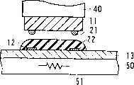
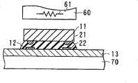
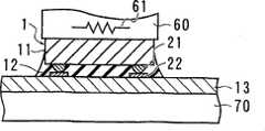
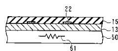
在各图中,符号1、2表示电气装置。符号12、15分别表示粘结剂。符号11表示半导体芯片。符号13表示基板(柔性布线板)。符号21表示半导体芯片的连接端子(凸点)。符号22表示基板的连接端子。符号50表示第一装载台(暂时压焊台)。符号70表示第二装载台(正式压焊台)。符号60表示挤压头(正式压焊头)。In each figure,
具体实施方式Detailed ways
现说明本发明的实施形态。Embodiments of the present invention will now be described.
首先,将作为热固化性树脂的环氧树脂、由微胶囊化的固化剂构成的潜在固化剂和导电粒子混合在一起,制作后述的表1的ACP、ACF、NCP各栏中示出的组成的粘结剂。在该状态下粘结剂呈膏状。First, an epoxy resin as a thermosetting resin, a latent curing agent composed of a microencapsulated curing agent, and conductive particles were mixed together to prepare the ACP, ACF, and NCP columns of Table 1 described later. composed of binders. In this state the adhesive is in the form of a paste.
图1(a)的符号13表示柔性布线板(基板)。在该柔性布线板13的表面上配置金属布线,从金属布线的一部分构成多个连接端子22。这些连接端子22分别露出于柔性布线板13的表面,分别配置于与后述半导体芯片的凸点对应的位置上。如将粘结剂12涂敷于装载后述半导体芯片的位置上,则柔性布线板13的连接端子22被粘结剂12覆盖(图1(b))。
图1(c)的符号50表示暂时压焊台(第一装载台)。在暂时压焊台50的表面附近配置陶瓷加热器51。如果用陶瓷加热器51将暂时压焊台50预先加热到至少是粘结剂12的反应开始温度以上,将柔性布线板13置于未配置连接端子22一侧的面之下,放置于暂时压焊台50的表面上,则柔性布线板13与粘结剂12借助于热传导被加热到反应开始温度以上。在该状态下调整陶瓷加热器51的通电量,使粘结剂12处于反应开始温度以上、反应峰值温度以下的温度(第一温度)。
这时,由于加热而粘结剂12的粘度降低,对粘结剂12的柔性布线板13的沾润性提高,所以在涂敷粘结剂12时被卷入了的气泡(空洞)消失。At this time, the viscosity of the adhesive 12 is lowered by heating, and the wettability of the
图1(d)的符号11表示半导体芯片。在半导体芯片11的一面上配置多个凸点21(连接端子),这些凸点21与半导体芯片11的未图示的内部电路进行电连接。
图1(d)的符号40表示保持机构,如图1(d)所示,在使配置了半导体芯片11的凸点21一侧的面朝下的状态下,利用保持机构40保持半导体芯片11,在使半导体芯片11位于柔性布线板13的上方的状态下,在进行了对位使半导体芯片11的凸点21与柔性布线板13的连接端子22互相相向后,使保持机构40下降,将半导体芯片11装在柔性布线板13上的粘结剂12上。The
如将半导体芯片11推压到半导体芯片11的凸点21不至与柔性布线板13的连接端子22相接的程度,则从凸点21的前端表面挤出粘结剂12,粘结剂12便流入邻接的凸点21之间的空隙。这时,由于粘结剂12的粘度因加热而比涂敷时降低,所以在粘结剂12流入凸点21之间时不产生空洞。If the
图2(a)示出了该状态,在半导体芯片11的凸点21之间空洞消失,粘结剂12被充填其中。另外,在互相相向的凸点21与连接端子22之间残留多余的粘结剂12,凸点21与连接端子22不进行电连接。另外,利用暂时压焊台50的陶瓷加热器51,粘结剂12的温度被维持在第一温度。FIG. 2( a ) shows the state where the voids disappear between the
通过将粘结剂12的温度维持在第一温度,潜在性固化剂的微胶囊局部地溶解,粘结剂的固化反应缓慢地进行。当粘结剂12的反应率达到2%以上、20%以下的范围时,在将半导体芯片11装到粘结剂12上的状态下,使保持机构退到上方,将柔性布线板13与粘结剂12、半导体芯片11一起从暂时压焊台50移到正式压焊台70(第二装载台)上(图2(b))。By maintaining the temperature of the adhesive 12 at the first temperature, the microcapsules of the latent curing agent are partially dissolved, and the curing reaction of the adhesive progresses slowly. When the reaction rate of the adhesive 12 reaches the range of 2% or more and 20% or less, in the state where the
在正式压焊台70的上方,配置正式压焊头(挤压头)60。在正式压焊头60中内置加热器61,正式压焊头60被预先加热到至少超过粘结剂12的反应峰值温度的温度。Above the main bonding table 70, the main bonding head (extrusion head) 60 is arranged. A
在图2(b)所示的状态下,虽然粘结剂12的粘度比涂敷时增高,但其流动性并未消失。In the state shown in FIG. 2(b), although the viscosity of the adhesive 12 is higher than that at the time of application, its fluidity does not disappear.
从而,将正式压焊头60压到粘结剂12上的半导体芯片11上,如果一边对正式压焊头60加热,一边施加规定的载重,则多余的粘结剂12与残留的空洞一起从凸点21与连接端子22之间被挤出,在粘结剂12被加热到反应峰值温度以上之前,凸点21被接到连接端子21上。Thereby, when the
在该状态下,如果进一步继续加热挤压,利用热传导将粘结剂12加热到反应峰值温度以上(第二温度),则粘结剂12中的潜在性固化剂完全溶解,粘结剂12的热固化反应急剧加快,在凸点21与连接端子22相接的状态下,粘结剂12完全固化。In this state, if further heating and extrusion is continued, and the adhesive 12 is heated above the reaction peak temperature (second temperature) by heat conduction, the latent curing agent in the adhesive 12 is completely dissolved, and the adhesive 12 The thermal curing reaction is rapidly accelerated, and the adhesive 12 is completely cured in a state where the
图2(c)示出了粘结剂12完全固化了的状态的电气装置1。在该电气装置1中,柔性布线板13与半导体芯片11用固化了的粘结剂12不仅进行机械连接,也经凸点21进行电连接。FIG. 2( c ) shows the
以上说明了使用膏状粘结剂12的情形,但本发明不限定于此。例如,也包含使本发明中所用的粘结剂半固化至表现出自支撑性的程度的膜状物,或添加固态树脂形成为膜状的物质。The case where the
图3(a)的符号15表示上述的膜状粘结剂之一例。如图3(b)所示,在将膜状粘结剂15贴附到配置了柔性布线板13的连接端子22一侧的面上以后,如在与图1(c)~图2(c)所示的工序相同的条件下分别进行暂时压焊工序和正式压焊工序,则得到如图3(c)所示的电气装置2。
[实施例][Example]
将下述表1中所示的环氧树脂、潜在性固化剂和导电粒子分别按下述表1中所示的比例混合,分别制作含有导电粒子的膏状粘结剂(ACP:各向异性导电膏)、含有导电粒子的膜状粘结剂(ACF:各向异性导电膜)和不含导电粒子的膏状粘结剂(NCP:非导电膏)。Mix the epoxy resin, latent curing agent, and conductive particles shown in the following Table 1 in the ratios shown in the following Table 1, respectively, to prepare paste adhesives containing conductive particles (ACP: anisotropic Conductive paste), film adhesive containing conductive particles (ACF: Anisotropic Conductive Film) and paste adhesive without conductive particles (NCP: Non-conductive paste).
表1:粘结剂的组成和配比Table 1: Composition and ratio of binder

*在上述表1中,ACP表示包含导电粒子的膏状粘结剂,ACF表示包含导电粒子的膜状粘结剂,NCP表示不包含导电粒子的膏状粘结剂。* In the above Table 1, ACP represents a paste-like adhesive containing conductive particles, ACF represents a film-like adhesive containing conductive particles, and NCP represents a paste-like adhesive containing no conductive particles.
*上述表1中的金属覆膜树脂粒子由在树脂粒子表面上形成镍镀层,又在该表面上形成金镀层的树脂粒子构成。*The metal-coated resin particles in Table 1 above consist of resin particles in which a nickel plating layer is formed on the surface of the resin particle and a gold plating layer is formed on the surface.
接着,在上述3种粘结剂之中,对于ACP而言,使用差示扫描热分析仪(精工电子工业(株)公司制,商品名为“DSC200”),以10℃/分钟的升温速度使之从30℃升温至250℃,进行差示扫描热分析。在图4中示出所得到的DSC曲线。Next, among the above-mentioned 3 kinds of binders, for ACP, using a differential scanning thermal analyzer (manufactured by Seiko Electronics Co., Ltd., trade name "DSC200"), the temperature was increased at a rate of 10°C/min. The temperature was raised from 30°C to 250°C, and differential scanning thermal analysis was performed. The resulting DSC curve is shown in FIG. 4 .
图4的横轴为温度(℃),纵轴为热流(mW),图4的符号D表示DSC曲线。另外,该图的符号B表示基线(底线)。The horizontal axis in FIG. 4 represents temperature (° C.), and the vertical axis represents heat flow (mW). Symbol D in FIG. 4 represents a DSC curve. In addition, the symbol B in this figure shows a base line (bottom line).
图4的符号S表示DSC曲线D从基线B上升的点(反应开始点),符号P表示DSC曲线的发热峰值位置(反应峰值点),反应开始点S在70℃,反应峰值点P在115.2℃。由于该DSC曲线D的发热峰与ACP的热固化反应有关,可知在对ACP加热时ACP的固化反应开始的温度为70℃(反应开始温度),固化反应达到峰值的温度(反应峰值温度)约为115℃。另外,在比反应峰值温度高的温度下,发热量急剧减少,固化反应大体结束。再有,这时的发热量:ACP每1mg时为442.9mJ。The symbol S in Figure 4 represents the point at which the DSC curve D rises from the baseline B (reaction start point), and the symbol P represents the heating peak position of the DSC curve (reaction peak point), the reaction start point S is at 70°C, and the reaction peak point P is at 115.2 ℃. Since the exothermic peak of the DSC curve D is related to the thermal curing reaction of ACP, it can be known that the temperature at which the curing reaction of ACP starts is 70°C (reaction initiation temperature) when ACP is heated, and the temperature at which the curing reaction reaches its peak value (reaction peak temperature) is about It is 115°C. In addition, at a temperature higher than the reaction peak temperature, the calorific value decreases rapidly, and the curing reaction is almost completed. Furthermore, the calorific value at this time: 442.9 mJ per 1 mg of ACP.
此外,采用粘度计(HAAKE公司制,商品名为“RheometerRS75”),测量使ACP以升温速度10℃/分钟从20℃升温至200℃时的粘度变化(粘度测量)。图5示出了从该测量结果得到的曲线,图5的横轴表示温度(℃),纵轴表示粘度(mPa·s)。Furthermore, using a viscometer (manufactured by HAAKE, trade name "Rheometer RS75"), the change in viscosity when ACP was heated from 20° C. to 200° C. at a temperature increase rate of 10° C./min was measured (viscosity measurement). FIG. 5 shows a graph obtained from the measurement results, and the horizontal axis of FIG. 5 represents temperature (° C.) and the vertical axis represents viscosity (mPa·s).
图5的符号S1表示与图4的反应开始点S对应的温度(反应开始温度),图5的符号P1表示与图4的反应峰值点P对应的温度(反应峰值温度)。从图5中所示的温度粘度曲线L1可知,加热粘结剂时的粘度在反应开始温度S1以上、反应峰值温度P1以下的范围内变得最低。另外,由于在反应峰值温度P1以上,粘结剂的固化反应加快,所以粘结剂的粘度急剧升高。The symbolS1 in FIG. 5 represents the temperature corresponding to the reaction start point S in FIG. 4 (reaction start temperature), and the symbolP1 in FIG. 5 represents the temperature corresponding to the reaction peak point P in FIG. 4 (reaction peak temperature). From the temperature-viscosity curveL1 shown in FIG. 5, it can be seen that the viscosity when the adhesive is heated becomes lowest in the range of the reaction start temperatureS1 or higher and the reaction peak temperature P1or lower. In addition, since the curing reaction of the adhesive accelerates above the reaction peak temperatureP1 , the viscosity of the adhesive rises sharply.
另外,关于ACF和NCP,分别测量了使之从20℃升温至200℃时的粘度变化。在图6中记载了ACF的温度粘度曲线L2,在图7中记载了NCP的温度粘度曲线L3。此外,用ACF、NCP进行了差示扫描热分析。在图6中记载了从差示扫描热分析得到的ACF的反应开始温度S2和反应峰值温度P2,在图7中记载了NCP的反应开始温度S3和反应峰值温度P3。In addition, about ACF and NCP, the viscosity change when it heated up from 20 degreeC to 200 degreeC was measured, respectively. FIG. 6 shows the temperature-viscosity curve L2 of ACF, and FIG. 7 shows the temperature-viscosity curve L3 of NCP. In addition, differential scanning thermal analysis was performed with ACF and NCP. The reaction start temperature S2 and the reaction peak temperature P2 of ACF obtained from differential scanning calorimetry are shown in FIG. 6 , and the reaction start temperature S3 and the reaction peak temperature P3 of NCP are shown in FIG. 7 .
从图6和图7可知,即使是将粘结剂形成为膜状的情况(ACF)或不含有导电粒子的情况(NCP),温度粘度曲线L2、L3的粘度成为最低的温度在反应开始温度S2、S3以上、反应峰值温度P2、P3以下的范围内。从这些结果确认了,当粘结剂为热固化性时,其粘度成为最低的温度在反应开始温度以上、反应峰值温度以下的范围内,而与其种类无关,在反应峰值温度以上,粘结剂的固化反应急剧加快。As can be seen from Fig. 6 and Fig. 7, even when the binder is formed into a film (ACF) or does not contain conductive particles (NCP), the temperature at which the viscosity of the temperature-viscosity curvesL2 andL3 becomes the lowest occurs at the reaction temperature. It is within the range of starting temperature S2 , S3 or higher, and reaction peak temperature P2 , P3 or lower. From these results, it was confirmed that when the binder is thermosetting, the temperature at which the viscosity becomes the lowest is in the range of above the reaction start temperature and below the reaction peak temperature, regardless of the type, and above the reaction peak temperature, the binder The curing reaction is rapidly accelerated.
接着,将上述3种粘结剂(ACP、ACF、NCP)分别涂敷或贴附在柔性布线板13上,在柔性布线板13装在暂时压焊台50上以后,加热暂时压焊台50,使各粘结剂12的温度上升到下述表2的“第一温度”一栏中所示的温度。接着,在图2(a)~图2(c)的工序中进行正式压焊,制作实施例1~7、比较例1~7的电气装置1。Next, the above-mentioned three kinds of adhesives (ACP, ACF, NCP) are respectively coated or pasted on the
表2:粘结剂的反应开始温度、反应峰值温度和各评价试验的结果Table 2: Reaction initiation temperature, reaction peak temperature, and results of each evaluation test of the binder

这里,作为柔性布线板13,采用在厚度20μm的聚酰亚胺膜的表面上配置了厚度12μm的金属布线(镀镍-金的铜布线)的布线板,作为半导体芯片11,采用在6mm见方的正方形形状、厚度0.4mm的芯片表面上配置了镀金凸点(60μm见方的正方形形状、高度20μm)的芯片。再有,在正式压焊工序中加热了的粘结剂12的温度(第二温度)为230℃,在正式压焊工序中所加的载重对每个凸点21为0.6N。Here, as the
采用这些实施例1~7、比较例1~7的电气装置1,分别进行了下面所示的“反应率”、空洞外观、“初始导通”、“老化后导通”的各评价试验。Using the
[反应率]在制造实施例1~7、比较例1~7的电气装置1的工序中,采用暂时压焊工序后的粘结剂12作为试料,对各试料采用与上述差示扫描热分析相同的方法进行差示扫描热分析,分别求得粘结剂的反应率。[Reaction rate] In the process of manufacturing the
这里,分别采用加热前(涂敷前)的粘结剂作为标准试料。Here, the adhesives before heating (before coating) were respectively used as standard samples.
在假定对标准试料以在进行差示扫描热分析时所测得的试料每1mg的发热量为A1,对试料(暂时压焊后的粘结剂)以在进行差示扫描热分析时所测得的试料每1mg的发热量为A2的情况下,用下式(1)得到的值被取作反应率R%。Assuming that the calorific value per 1 mg of the sample measured during the differential scanning thermal analysis is A1 for the standard sample, the sample (adhesive after temporary pressure welding) is measured in the differential scanning thermal analysis When the calorific value per 1 mg of the sample measured at the time of analysis isA2 , the value obtained by the following formula (1) is taken as the reaction rate R%.
R(%)=(1-A2/A1)×100......式(1)R(%)=(1-A2 /A1 )×100...Formula (1)
在上述表2中记载了各反应率。The respective reaction rates are described in Table 2 above.
[空洞外观]对于实施例1~7、比较例1~7的电气装置1,用金属显微镜观察与配置了柔性布线板13的半导体芯片11一侧相反的一侧的面,确认在将凸点21与连接端子22相接的部分即连接部的周围的空洞的有无。[Void Appearance] Regarding the
这时,假定未观察到比凸点21大的空洞的场合为“○”,观察到比凸点21大的空洞的场合为“×”,进行了评价。在上述表2中记载了这些评价结果。At this time, evaluation was performed assuming that "◯" was observed when no void larger than the
[初始导通]对于实施例1~7、比较例1~7的电气装置1,分别测量了连接凸点21的2个连接端子22之间的导通电阻值。假定导通电阻值在100mΩ以下的场合为“○”,在100mΩ以上的场合为“×”,进行了评价。在上述表2中记载了这些评价结果。[Initial Conduction] Regarding the
[老化后导通]将实施例1~7、比较例1~7的电气装置1在121℃、相对湿度100%的高温高湿条件下放置了100小时(老化)后,采用与上述“初始导通”相同的方法测量了导通电阻值。假定导通电阻值在500mΩ以下的场合为“○”,在500mΩ以上的场合为“×”,进行了评价。在上述表2中记载了这些评价结果。[Continuation after Aging] After placing the
从上述表2可知,在暂时压焊前的粘结剂的加热温度(第一温度)为反应开始温度以上、反应峰值温度以下的实施例1~7的电气装置1中,对各评价试验得到优秀的结果。As can be seen from the above Table 2, in the
另一方面,在暂时压焊前未进行加热的比较例1的电气装置及第温度低于各粘结剂的反应开始温度的比较例2、4、6中,由于暂时压焊前粘结剂的粘度并不充分地低,所以连接部周围的粘结剂中存在大量空洞,其结果是,老化后的导通结果变坏。On the other hand, in the electrical device of Comparative Example 1 that was not heated before temporary pressure welding, and in Comparative Examples 2, 4, and 6 where the first temperature was lower than the reaction start temperature of each adhesive, the adhesive before temporary pressure welding The viscosity is not sufficiently low, so there are a lot of voids in the adhesive around the connection part, as a result, the conduction result after aging is deteriorated.
另外,在暂时压焊前的温度分别比各粘结剂的反应峰值温度高的比较例3、5、7中,在粘结剂中未观察到大的空洞,但由于在正式压焊前粘结剂的粘度过高,粘结剂无法充分地挤出去,所以在连接端子与凸点之间不能充分地取得导通,在老化前的初始导通阶段被确认为导通不良。In addition, in Comparative Examples 3, 5, and 7 in which the temperature before tentative bonding was higher than the reaction peak temperature of each adhesive, no large voids were observed in the adhesive, but due to the adhesion before actual bonding The viscosity of the bonding agent is too high, and the adhesive cannot be squeezed out sufficiently, so sufficient conduction cannot be obtained between the connection terminal and the bump, and it is confirmed as poor conduction in the initial conduction stage before aging.
以上说明了将暂时压焊工序与正式压焊工序在各不相同的平台上进行的情况,但本发明却不限定于此,可在同一平台上进行暂时压焊工序和正式压焊工序。另外,将粘结剂涂敷在基板上的工序也可在暂时压焊平台上进行。The above describes the case where the temporary bonding process and the main bonding process are performed on different platforms, but the present invention is not limited thereto, and the temporary bonding process and the main bonding process may be performed on the same platform. In addition, the process of applying the adhesive to the substrate can also be performed on the temporary bonding platform.
另外,以上说明了使暂时压焊平台50升温将粘结剂12加热到第一温度的情况,但本发明却不限定于此,可采用各种加热装置。例如,使保持机构40内内置加热装置,同时借助于在加热炉内进行暂时压焊工序,可将粘结剂12加热到第一温度。In addition, the case where the temperature of the
另外,如果使正式压焊平台内内置加热装置,利用加热装置预先加热正式压焊平台,则由于在将柔性布线板13从暂时压焊平台50移到正式压焊平台时,粘结剂12的温度不降低,所以可更加缩短在正式压焊工序中花费的时间。这时,希望正式压焊平台的温度在第二温度以下,如为第一温度左右则更好。In addition, if the heating device is built into the formal bonding platform, and the formal bonding platform is heated in advance by the heating device, since the
以上说明了将半导体芯11与柔性布线板13连接起来的情况,但本发明却不限定于此,可用于各种电气装置的制造。例如,也可不用柔性布线板而用刚性基板,将刚性基板与半导体芯片连接起来,制作COB(芯片在基板上)。The case where the
另外,也可用于TCP(带式载体封装)与LCD(液晶显示器件)的连接。In addition, it can also be used for the connection between TCP (tape carrier package) and LCD (liquid crystal display device).
图8的符号80表示电气装置,电气装置80具有TCP83和LCD81。图8的符号84表示用TCP83的布线的一部分构成的连接端子,图8的符号82表示用LCD81的电极的一部分构成的连接端子。
TCP83与LCD81用与上述图1(a)~图1(d)、图2(a)~图2(c)相同的工序连接起来,连接端子82、84在相互接触的状态下用粘结剂85加以固定。TCP83 and LCD81 are connected by the same process as above-mentioned Fig. 1(a)-Fig. 1(d), Fig. 2(a)-Fig. 85 to be fixed.
作为可用于本发明的热固化性树脂,可使用环氧树脂、尿素树脂、蜜胺树脂、酚醛树脂等各种树脂,但如考虑到固化速度及热固化后的粘结剂强度等,最好用环氧树脂。As the thermosetting resin that can be used in the present invention, various resins such as epoxy resin, urea resin, melamine resin, and phenolic resin can be used, but considering the curing speed and the adhesive strength after thermosetting, etc., Use epoxy.
在使用环氧树脂作为热固化树脂时,最好并用固化剂。作为固化剂可用咪唑类固化剂、聚胺固化剂、酚醛类、异氰酸酯类、聚When using an epoxy resin as a thermosetting resin, it is preferable to use a curing agent together. As the curing agent, imidazole curing agent, polyamine curing agent, phenolic, isocyanate, poly
硫醇类、酸酐固化剂等各种固化剂。将这些固化剂制成微胶囊,可用作潜在性固化剂。Various curing agents such as mercaptans and acid anhydride curing agents. These curing agents are microencapsulated and can be used as latent curing agents.
另外,向粘结剂添加热塑性树脂也是可能的。作为热塑性树脂,可使用苯氧基树脂、聚酯树脂等各种树脂。In addition, it is also possible to add a thermoplastic resin to the binder. As the thermoplastic resin, various resins such as phenoxy resins and polyester resins can be used.
也可向本发明中使用的粘结剂中添加消泡剂、着色剂、防老化剂、充填剂、偶联剂等各种添加剂。Various additives such as defoamers, colorants, anti-aging agents, fillers, and coupling agents can also be added to the binder used in the present invention.
工业上的可利用性Industrial availability
在使半导体芯片与基板上的粘结剂相接的暂时压焊时,粘结剂中不发生空洞。另外,即使在暂时压焊后残留有空洞时,为了增高正式压焊时粘结剂的粘度,可用挤压法挤出粘结剂中的空洞。从而,按照本发明,在粘结剂中空洞消失,可得到导通可靠性高的电气装置。During temporary pressure bonding for bringing the semiconductor chip into contact with the adhesive on the substrate, voids do not occur in the adhesive. In addition, even if voids remain after temporary pressure welding, in order to increase the viscosity of the adhesive during the main pressure welding, the voids in the adhesive can be squeezed out by extrusion. Therefore, according to the present invention, voids are eliminated in the adhesive, and an electrical device with high conduction reliability can be obtained.
Claims (13)
Applications Claiming Priority (2)
| Application Number | Priority Date | Filing Date | Title |
|---|---|---|---|
| JP2001049615AJP3665579B2 (en) | 2001-02-26 | 2001-02-26 | Electrical device manufacturing method |
| JP49615/2001 | 2001-02-26 |
Publications (2)
| Publication Number | Publication Date |
|---|---|
| CN1505835A CN1505835A (en) | 2004-06-16 |
| CN100392832Ctrue CN100392832C (en) | 2008-06-04 |
Family
ID=18910693
Family Applications (1)
| Application Number | Title | Priority Date | Filing Date |
|---|---|---|---|
| CNB028087933AExpired - LifetimeCN100392832C (en) | 2001-02-26 | 2002-02-15 | Electrical device manufacturing method |
Country Status (6)
| Country | Link |
|---|---|
| US (1) | US7341642B2 (en) |
| JP (1) | JP3665579B2 (en) |
| KR (1) | KR100790671B1 (en) |
| CN (1) | CN100392832C (en) |
| TW (1) | TW523885B (en) |
| WO (1) | WO2002071469A1 (en) |
Families Citing this family (61)
| Publication number | Priority date | Publication date | Assignee | Title |
|---|---|---|---|---|
| JP4206320B2 (en)* | 2003-09-19 | 2009-01-07 | 株式会社ルネサステクノロジ | Manufacturing method of semiconductor integrated circuit device |
| US20080055581A1 (en)* | 2004-04-27 | 2008-03-06 | Rogers John A | Devices and methods for pattern generation by ink lithography |
| CN103646848B (en) | 2004-06-04 | 2018-06-05 | 伊利诺伊大学评议会 | The method of assembling printable semiconductor elements and manufacture electronic device |
| US7943491B2 (en)* | 2004-06-04 | 2011-05-17 | The Board Of Trustees Of The University Of Illinois | Pattern transfer printing by kinetic control of adhesion to an elastomeric stamp |
| US7521292B2 (en) | 2004-06-04 | 2009-04-21 | The Board Of Trustees Of The University Of Illinois | Stretchable form of single crystal silicon for high performance electronics on rubber substrates |
| US7799699B2 (en) | 2004-06-04 | 2010-09-21 | The Board Of Trustees Of The University Of Illinois | Printable semiconductor structures and related methods of making and assembling |
| US8217381B2 (en)* | 2004-06-04 | 2012-07-10 | The Board Of Trustees Of The University Of Illinois | Controlled buckling structures in semiconductor interconnects and nanomembranes for stretchable electronics |
| CH697279B1 (en)* | 2004-12-06 | 2008-07-31 | Oerlikon Assembly Equipment Ag | A method for mounting a semiconductor chip on a substrate. |
| JP4692544B2 (en)* | 2005-04-14 | 2011-06-01 | パナソニック株式会社 | Electronic circuit device and manufacturing method thereof |
| JP4621595B2 (en)* | 2006-01-11 | 2011-01-26 | 株式会社東芝 | Manufacturing method of semiconductor device |
| EP1991723A2 (en) | 2006-03-03 | 2008-11-19 | The Board Of Trustees Of The University Of Illinois | Methods of making spatially aligned nanotubes and nanotube arrays |
| JP5020629B2 (en) | 2006-12-28 | 2012-09-05 | パナソニック株式会社 | How to connect electronic components |
| EP2104954B1 (en) | 2007-01-17 | 2022-03-16 | The Board of Trustees of the University of Illinois | Optical systems fabricated by printing-based assembly |
| JP2008209961A (en)* | 2007-02-23 | 2008-09-11 | Fujitsu Ltd | Method for manufacturing electronic device, method for manufacturing electronic device mounted with electronic device, and method for manufacturing article mounted with electronic device |
| WO2009001605A1 (en)* | 2007-06-26 | 2008-12-31 | Sony Chemical & Information Device Corporation | Anisotropic elctroconductive material, connection structure, and process for producing the connection structure |
| JP5093482B2 (en)* | 2007-06-26 | 2012-12-12 | ソニーケミカル&インフォメーションデバイス株式会社 | Anisotropic conductive material, connection structure and manufacturing method thereof |
| JP4998732B2 (en)* | 2007-10-22 | 2012-08-15 | ソニーケミカル&インフォメーションデバイス株式会社 | Anisotropic conductive adhesive |
| JP2009105276A (en)* | 2007-10-24 | 2009-05-14 | Omron Corp | Semiconductor chip mounting method and semiconductor mounting wiring board |
| TWI723953B (en) | 2008-03-05 | 2021-04-11 | 美國伊利諾大學理事會 | Stretchable and foldable electronic devices |
| US8470701B2 (en)* | 2008-04-03 | 2013-06-25 | Advanced Diamond Technologies, Inc. | Printable, flexible and stretchable diamond for thermal management |
| US8946683B2 (en)* | 2008-06-16 | 2015-02-03 | The Board Of Trustees Of The University Of Illinois | Medium scale carbon nanotube thin film integrated circuits on flexible plastic substrates |
| US8886334B2 (en) | 2008-10-07 | 2014-11-11 | Mc10, Inc. | Systems, methods, and devices using stretchable or flexible electronics for medical applications |
| US8097926B2 (en) | 2008-10-07 | 2012-01-17 | Mc10, Inc. | Systems, methods, and devices having stretchable integrated circuitry for sensing and delivering therapy |
| US8372726B2 (en)* | 2008-10-07 | 2013-02-12 | Mc10, Inc. | Methods and applications of non-planar imaging arrays |
| US8389862B2 (en) | 2008-10-07 | 2013-03-05 | Mc10, Inc. | Extremely stretchable electronics |
| JP5646492B2 (en)* | 2008-10-07 | 2014-12-24 | エムシー10 インコーポレイテッドMc10,Inc. | Stretchable integrated circuit and device with sensor array |
| EP2430652B1 (en) | 2009-05-12 | 2019-11-20 | The Board of Trustees of the University of Illionis | Printed assemblies of ultrathin, microscale inorganic light emitting diodes for deformable and semitransparent displays |
| EP2466631A1 (en)* | 2009-09-30 | 2012-06-20 | Sharp Kabushiki Kaisha | Substrate module and manufacturing method thereof |
| WO2011041727A1 (en) | 2009-10-01 | 2011-04-07 | Mc10, Inc. | Protective cases with integrated electronics |
| US10918298B2 (en) | 2009-12-16 | 2021-02-16 | The Board Of Trustees Of The University Of Illinois | High-speed, high-resolution electrophysiology in-vivo using conformal electronics |
| US10441185B2 (en) | 2009-12-16 | 2019-10-15 | The Board Of Trustees Of The University Of Illinois | Flexible and stretchable electronic systems for epidermal electronics |
| US9936574B2 (en) | 2009-12-16 | 2018-04-03 | The Board Of Trustees Of The University Of Illinois | Waterproof stretchable optoelectronics |
| EP2547258B1 (en) | 2010-03-17 | 2015-08-05 | The Board of Trustees of the University of Illionis | Implantable biomedical devices on bioresorbable substrates |
| KR101670887B1 (en) | 2010-03-22 | 2016-11-10 | 삼성디스플레이 주식회사 | Electro-phoretic display device and method for manufacturing the same |
| JP5586313B2 (en)* | 2010-04-23 | 2014-09-10 | 京セラケミカル株式会社 | Method for forming adhesive layer and adhesive composition |
| RU2563971C2 (en)* | 2010-10-14 | 2015-09-27 | Стора Энсо Ойй | Method and device of connecting chip to printed conductive surface |
| US9442285B2 (en) | 2011-01-14 | 2016-09-13 | The Board Of Trustees Of The University Of Illinois | Optical component array having adjustable curvature |
| US9765934B2 (en) | 2011-05-16 | 2017-09-19 | The Board Of Trustees Of The University Of Illinois | Thermally managed LED arrays assembled by printing |
| JP2014523633A (en) | 2011-05-27 | 2014-09-11 | エムシー10 インコーポレイテッド | Electronic, optical and / or mechanical devices and systems and methods of manufacturing these devices and systems |
| WO2012167096A2 (en) | 2011-06-03 | 2012-12-06 | The Board Of Trustees Of The University Of Illinois | Conformable actively multiplexed high-density surface electrode array for brain interfacing |
| US9555644B2 (en)* | 2011-07-14 | 2017-01-31 | The Board Of Trustees Of The University Of Illinois | Non-contact transfer printing |
| KR101979354B1 (en) | 2011-12-01 | 2019-08-29 | 더 보오드 오브 트러스티스 오브 더 유니버시티 오브 일리노이즈 | Transient devices designed to undergo programmable transformations |
| KR101403865B1 (en)* | 2011-12-16 | 2014-06-10 | 제일모직주식회사 | Composition for use in an anisotropic conductive film, an anisotropic conductive film and semiconductor device |
| KR101395707B1 (en)* | 2011-12-16 | 2014-05-15 | 제일모직주식회사 | Adhesive film for semiconductor |
| JP2015521303A (en) | 2012-03-30 | 2015-07-27 | ザ ボード オブ トラスティーズ オブ ザ ユニヴァーシ | An electronic device that can be attached to the surface and can be attached to an accessory |
| JP5857233B2 (en)* | 2012-04-10 | 2016-02-10 | パナソニックIpマネジメント株式会社 | Electrode bonding method, electrode bonding structure manufacturing method, and electrode bonding structure manufacturing system |
| JP5978725B2 (en)* | 2012-04-11 | 2016-08-24 | 日立化成株式会社 | Manufacturing method of semiconductor device |
| CN104221480B (en)* | 2012-04-19 | 2017-09-08 | 松下知识产权经营株式会社 | Electronic component mounting method and electronic component hookup wire |
| JP5851952B2 (en)* | 2012-07-19 | 2016-02-03 | ルネサスエレクトロニクス株式会社 | Manufacturing method of semiconductor device |
| US9209155B2 (en)* | 2012-08-06 | 2015-12-08 | Sekisui Chemical Co., Ltd. | Method for manufacturing semiconductor device and adhesive for mounting flip chip |
| US9171794B2 (en) | 2012-10-09 | 2015-10-27 | Mc10, Inc. | Embedding thin chips in polymer |
| KR101551758B1 (en)* | 2012-12-11 | 2015-09-09 | 제일모직주식회사 | Composition for use of an anisotropic conductive film and an anisotropic conductive film thereof |
| WO2015004830A1 (en) | 2013-07-08 | 2015-01-15 | ソニー株式会社 | Method for determining curing conditions, method for producing circuit device, and circuit device |
| JP6438790B2 (en)* | 2015-02-06 | 2018-12-19 | デクセリアルズ株式会社 | Semiconductor device manufacturing method and underfill film |
| KR101949632B1 (en)* | 2015-03-26 | 2019-02-18 | 데쿠세리아루즈 가부시키가이샤 | Method for manufacturing flexible mounting module body |
| AU2016270807A1 (en) | 2015-06-01 | 2017-12-14 | The Board Of Trustees Of The University Of Illinois | Miniaturized electronic systems with wireless power and near-field communication capabilities |
| MX2017015587A (en) | 2015-06-01 | 2018-08-23 | Univ Illinois | Alternative approach to uv sensing. |
| US10925543B2 (en) | 2015-11-11 | 2021-02-23 | The Board Of Trustees Of The University Of Illinois | Bioresorbable silicon electronics for transient implants |
| KR102429619B1 (en)* | 2015-11-18 | 2022-08-04 | 삼성전자주식회사 | Bonding stage and bonding apparatus comprising the same |
| CN108039415B (en)* | 2017-11-02 | 2019-06-07 | 厦门市三安光电科技有限公司 | The packaging method of microcomponent |
| CN109887849A (en)* | 2019-01-31 | 2019-06-14 | 通富微电子股份有限公司 | A kind of method and system of cooling fin pasting chip |
Citations (7)
| Publication number | Priority date | Publication date | Assignee | Title |
|---|---|---|---|---|
| JPH02226738A (en)* | 1989-02-28 | 1990-09-10 | Toshiba Corp | Carrier tape component mounting equipment |
| JPH04302444A (en)* | 1991-03-29 | 1992-10-26 | Toshiba Corp | Mounting method of semiconductor elements |
| CN1132931A (en)* | 1994-12-30 | 1996-10-09 | 卡西欧计算机公司 | Method of connecting terminals of one electronic part to terminals of another electronic part |
| CN1191326A (en)* | 1997-02-19 | 1998-08-26 | 阿尔卑斯电气株式会社 | Apparatus and method for installing electric parts |
| JPH11330162A (en)* | 1998-05-19 | 1999-11-30 | Sony Corp | Mounting of semiconductor chip |
| JP2000113919A (en)* | 1998-08-03 | 2000-04-21 | Sony Corp | Electrical connection device and electrically connecting method |
| JP2001024032A (en)* | 1999-07-06 | 2001-01-26 | Toppan Printing Co Ltd | IC chip mounting method and device for contactless IC card |
Family Cites Families (3)
| Publication number | Priority date | Publication date | Assignee | Title |
|---|---|---|---|---|
| JP2830852B2 (en) | 1996-08-08 | 1998-12-02 | 松下電器産業株式会社 | Electronic component mounting method |
| US6077382A (en)* | 1997-05-09 | 2000-06-20 | Citizen Watch Co., Ltd | Mounting method of semiconductor chip |
| US7244675B2 (en)* | 2000-03-23 | 2007-07-17 | Sony Corporation | Electrical connection materials and electrical connection method |
- 2001
- 2001-02-26JPJP2001049615Apatent/JP3665579B2/ennot_activeExpired - Lifetime
- 2002
- 2002-02-15WOPCT/JP2002/001284patent/WO2002071469A1/enactiveApplication Filing
- 2002-02-15KRKR1020037011127Apatent/KR100790671B1/ennot_activeExpired - Lifetime
- 2002-02-15CNCNB028087933Apatent/CN100392832C/ennot_activeExpired - Lifetime
- 2002-02-19TWTW091102771Apatent/TW523885B/ennot_activeIP Right Cessation
- 2003
- 2003-08-25USUS10/647,448patent/US7341642B2/ennot_activeExpired - Lifetime
Patent Citations (7)
| Publication number | Priority date | Publication date | Assignee | Title |
|---|---|---|---|---|
| JPH02226738A (en)* | 1989-02-28 | 1990-09-10 | Toshiba Corp | Carrier tape component mounting equipment |
| JPH04302444A (en)* | 1991-03-29 | 1992-10-26 | Toshiba Corp | Mounting method of semiconductor elements |
| CN1132931A (en)* | 1994-12-30 | 1996-10-09 | 卡西欧计算机公司 | Method of connecting terminals of one electronic part to terminals of another electronic part |
| CN1191326A (en)* | 1997-02-19 | 1998-08-26 | 阿尔卑斯电气株式会社 | Apparatus and method for installing electric parts |
| JPH11330162A (en)* | 1998-05-19 | 1999-11-30 | Sony Corp | Mounting of semiconductor chip |
| JP2000113919A (en)* | 1998-08-03 | 2000-04-21 | Sony Corp | Electrical connection device and electrically connecting method |
| JP2001024032A (en)* | 1999-07-06 | 2001-01-26 | Toppan Printing Co Ltd | IC chip mounting method and device for contactless IC card |
Also Published As
| Publication number | Publication date |
|---|---|
| KR100790671B1 (en) | 2007-12-31 |
| CN1505835A (en) | 2004-06-16 |
| US20040079464A1 (en) | 2004-04-29 |
| US7341642B2 (en) | 2008-03-11 |
| JP2002252254A (en) | 2002-09-06 |
| WO2002071469A1 (en) | 2002-09-12 |
| JP3665579B2 (en) | 2005-06-29 |
| HK1064804A1 (en) | 2005-02-04 |
| KR20030080035A (en) | 2003-10-10 |
| TW523885B (en) | 2003-03-11 |
Similar Documents
| Publication | Publication Date | Title |
|---|---|---|
| CN100392832C (en) | Electrical device manufacturing method | |
| JP5311772B2 (en) | Adhesive film | |
| TWI480966B (en) | Method of manufacturing a connecting structure | |
| KR100384314B1 (en) | Method and device for mounting electronic component on circuit board | |
| CN101322233B (en) | Method of bonding between electrical devices using ultrasonic vibration | |
| KR101150613B1 (en) | Adhesive film, connecting method, and joined structure | |
| KR100563890B1 (en) | Electrical connecting device and electrical connecting method | |
| JP2003282636A (en) | Method for producing connection structure | |
| US6376050B1 (en) | Electric connecting method and apparatus | |
| CN119300260A (en) | Method for manufacturing connector and connector | |
| US12418153B2 (en) | Method for manufacturing connection body, and connection body | |
| KR20120022580A (en) | Manufacturing method of mounting device, connecting method and anisotropic conductive film | |
| CN113728402B (en) | Connection structure, method for manufacturing connection structure, connection material, and coated conductive particle | |
| KR102106996B1 (en) | Component mounting method using sheet containing solder particles | |
| JP4197026B2 (en) | Multi-chip mounting method | |
| KR100248582B1 (en) | Connection sheet for mutually connecting the electrodes facing each other, and electrode connection structure and connection method using the connection sheet | |
| JP4378788B2 (en) | IC chip connection method | |
| JP3148008B2 (en) | Method of connecting substrate and chip using conductive adhesive | |
| JP3750606B2 (en) | Manufacturing method of semiconductor device | |
| JP2003249287A (en) | Anisotropically conductive adhesive, heat seal connector and connection structure | |
| JP2000011760A (en) | Anisotropic conductive composition and manufacture of anisotropic conductive member using it | |
| JP4595981B2 (en) | Connection member, electrode connection structure and connection method using the connection member | |
| HK1064804B (en) | Electric device producing method | |
| JP3449904B2 (en) | Adhesive composition | |
| JP2000174066A (en) | Semiconductor device mounting method |
Legal Events
| Date | Code | Title | Description |
|---|---|---|---|
| C06 | Publication | ||
| PB01 | Publication | ||
| C10 | Entry into substantive examination | ||
| SE01 | Entry into force of request for substantive examination | ||
| REG | Reference to a national code | Ref country code:HK Ref legal event code:DE Ref document number:1064804 Country of ref document:HK | |
| C14 | Grant of patent or utility model | ||
| GR01 | Patent grant | ||
| REG | Reference to a national code | Ref country code:HK Ref legal event code:GR Ref document number:1064804 Country of ref document:HK | |
| CX01 | Expiry of patent term | Granted publication date:20080604 | |
| CX01 | Expiry of patent term |