CN100388419C - Method for forming trench capacitor on substrate and trench capacitor - Google Patents
Method for forming trench capacitor on substrate and trench capacitorDownload PDFInfo
- Publication number
- CN100388419C CN100388419CCNB200510118408XACN200510118408ACN100388419CCN 100388419 CCN100388419 CCN 100388419CCN B200510118408X ACNB200510118408X ACN B200510118408XACN 200510118408 ACN200510118408 ACN 200510118408ACN 100388419 CCN100388419 CCN 100388419C
- Authority
- CN
- China
- Prior art keywords
- substrate
- separator
- electrode
- channel capacitor
- groove
- Prior art date
- Legal status (The legal status is an assumption and is not a legal conclusion. Google has not performed a legal analysis and makes no representation as to the accuracy of the status listed.)
- Expired - Fee Related
Links
- 239000000758substrateSubstances0.000titleclaimsabstractdescription125
- 239000003990capacitorSubstances0.000titleclaimsabstractdescription108
- 238000000034methodMethods0.000titleclaimsabstractdescription49
- 238000002955isolationMethods0.000claimsabstractdescription53
- 230000002093peripheral effectEffects0.000claimsabstractdescription7
- 230000015572biosynthetic processEffects0.000claimsdescription20
- IJGRMHOSHXDMSA-UHFFFAOYSA-NAtomic nitrogenChemical compoundN#NIJGRMHOSHXDMSA-UHFFFAOYSA-N0.000claimsdescription14
- 229910052581Si3N4Inorganic materials0.000claimsdescription12
- HQVNEWCFYHHQES-UHFFFAOYSA-Nsilicon nitrideChemical compoundN12[Si]34N5[Si]62N3[Si]51N64HQVNEWCFYHHQES-UHFFFAOYSA-N0.000claimsdescription12
- XUIMIQQOPSSXEZ-UHFFFAOYSA-NSiliconChemical compound[Si]XUIMIQQOPSSXEZ-UHFFFAOYSA-N0.000claimsdescription9
- 229910021420polycrystalline siliconInorganic materials0.000claimsdescription9
- 229920005591polysiliconPolymers0.000claimsdescription9
- 229910052710siliconInorganic materials0.000claimsdescription9
- 239000010703siliconSubstances0.000claimsdescription9
- 229910052785arsenicInorganic materials0.000claimsdescription8
- RQNWIZPPADIBDY-UHFFFAOYSA-Narsenic atomChemical compound[As]RQNWIZPPADIBDY-UHFFFAOYSA-N0.000claimsdescription8
- VYPSYNLAJGMNEJ-UHFFFAOYSA-NSilicium dioxideChemical compoundO=[Si]=OVYPSYNLAJGMNEJ-UHFFFAOYSA-N0.000claimsdescription7
- 229910052757nitrogenInorganic materials0.000claimsdescription7
- QVGXLLKOCUKJST-UHFFFAOYSA-Natomic oxygenChemical compound[O]QVGXLLKOCUKJST-UHFFFAOYSA-N0.000claimsdescription6
- 229910052760oxygenInorganic materials0.000claimsdescription6
- 239000001301oxygenSubstances0.000claimsdescription6
- 238000009792diffusion processMethods0.000claimsdescription5
- 230000003647oxidationEffects0.000claimsdescription5
- 238000007254oxidation reactionMethods0.000claimsdescription5
- 239000012535impuritySubstances0.000claimsdescription4
- 229910052751metalInorganic materials0.000claimsdescription3
- 239000002184metalSubstances0.000claimsdescription3
- 239000011521glassSubstances0.000claims12
- OAICVXFJPJFONN-UHFFFAOYSA-NPhosphorusChemical compound[P]OAICVXFJPJFONN-UHFFFAOYSA-N0.000claims1
- 229910045601alloyInorganic materials0.000claims1
- 239000000956alloySubstances0.000claims1
- 229910052698phosphorusInorganic materials0.000claims1
- 239000011574phosphorusSubstances0.000claims1
- 239000000377silicon dioxideSubstances0.000claims1
- 230000015654memoryEffects0.000description29
- 238000013461designMethods0.000description17
- 238000005530etchingMethods0.000description12
- 230000003071parasitic effectEffects0.000description7
- 238000005229chemical vapour depositionMethods0.000description6
- 238000005137deposition processMethods0.000description6
- 239000004065semiconductorSubstances0.000description6
- 238000002513implantationMethods0.000description5
- 230000014759maintenance of locationEffects0.000description5
- 239000000463materialSubstances0.000description5
- 229910052814silicon oxideInorganic materials0.000description5
- 238000000137annealingMethods0.000description4
- 239000002019doping agentSubstances0.000description4
- 238000004519manufacturing processMethods0.000description4
- 229920002120photoresistant polymerPolymers0.000description4
- 239000004020conductorSubstances0.000description3
- 239000003989dielectric materialSubstances0.000description3
- 238000004518low pressure chemical vapour depositionMethods0.000description3
- 239000005360phosphosilicate glassSubstances0.000description3
- 238000003860storageMethods0.000description3
- ZOKXTWBITQBERF-UHFFFAOYSA-NMolybdenumChemical compound[Mo]ZOKXTWBITQBERF-UHFFFAOYSA-N0.000description2
- 238000011161developmentMethods0.000description2
- 230000000694effectsEffects0.000description2
- 230000005669field effectEffects0.000description2
- 125000001475halogen functional groupChemical group0.000description2
- 229910052750molybdenumInorganic materials0.000description2
- 239000011733molybdenumSubstances0.000description2
- 230000001590oxidative effectEffects0.000description2
- 238000000059patterningMethods0.000description2
- ZOXJGFHDIHLPTG-UHFFFAOYSA-NBoronChemical compound[B]ZOXJGFHDIHLPTG-UHFFFAOYSA-N0.000description1
- BPQQTUXANYXVAA-UHFFFAOYSA-NOrthosilicateChemical compound[O-][Si]([O-])([O-])[O-]BPQQTUXANYXVAA-UHFFFAOYSA-N0.000description1
- 229910000577Silicon-germaniumInorganic materials0.000description1
- LEVVHYCKPQWKOP-UHFFFAOYSA-N[Si].[Ge]Chemical compound[Si].[Ge]LEVVHYCKPQWKOP-UHFFFAOYSA-N0.000description1
- 230000004888barrier functionEffects0.000description1
- 229910052796boronInorganic materials0.000description1
- 238000000151depositionMethods0.000description1
- 230000008021depositionEffects0.000description1
- 238000005265energy consumptionMethods0.000description1
- 238000011049fillingMethods0.000description1
- 239000007943implantSubstances0.000description1
- 239000011810insulating materialSubstances0.000description1
- 238000009413insulationMethods0.000description1
- 238000012986modificationMethods0.000description1
- 230000004048modificationEffects0.000description1
- 229910021421monocrystalline siliconInorganic materials0.000description1
- 150000004767nitridesChemical class0.000description1
- 238000011160researchMethods0.000description1
- 238000000926separation methodMethods0.000description1
- 239000005368silicate glassSubstances0.000description1
- 229910021332silicideInorganic materials0.000description1
- FVBUAEGBCNSCDD-UHFFFAOYSA-Nsilicide(4-)Chemical compound[Si-4]FVBUAEGBCNSCDD-UHFFFAOYSA-N0.000description1
- 230000001360synchronised effectEffects0.000description1
- 238000007669thermal treatmentMethods0.000description1
- WFKWXMTUELFFGS-UHFFFAOYSA-NtungstenChemical compound[W]WFKWXMTUELFFGS-UHFFFAOYSA-N0.000description1
- 229910052721tungstenInorganic materials0.000description1
- 239000010937tungstenSubstances0.000description1
- -1tungtenSubstances0.000description1
- 238000001039wet etchingMethods0.000description1
Images


Classifications
- H—ELECTRICITY
- H10—SEMICONDUCTOR DEVICES; ELECTRIC SOLID-STATE DEVICES NOT OTHERWISE PROVIDED FOR
- H10D—INORGANIC ELECTRIC SEMICONDUCTOR DEVICES
- H10D1/00—Resistors, capacitors or inductors
- H10D1/60—Capacitors
- H10D1/62—Capacitors having potential barriers
- H10D1/66—Conductor-insulator-semiconductor capacitors, e.g. MOS capacitors
- H10D1/665—Trench conductor-insulator-semiconductor capacitors, e.g. trench MOS capacitors
- H—ELECTRICITY
- H10—SEMICONDUCTOR DEVICES; ELECTRIC SOLID-STATE DEVICES NOT OTHERWISE PROVIDED FOR
- H10B—ELECTRONIC MEMORY DEVICES
- H10B12/00—Dynamic random access memory [DRAM] devices
- H10B12/01—Manufacture or treatment
- H10B12/02—Manufacture or treatment for one transistor one-capacitor [1T-1C] memory cells
- H10B12/03—Making the capacitor or connections thereto
- H10B12/038—Making the capacitor or connections thereto the capacitor being in a trench in the substrate
- H10B12/0387—Making the trench
Landscapes
- Engineering & Computer Science (AREA)
- Manufacturing & Machinery (AREA)
- Semiconductor Memories (AREA)
- Semiconductor Integrated Circuits (AREA)
Abstract
Description
Translated fromChinese技术领域technical field
本发明涉及半导体元件,特别有关于具有埋入隔离层的沟槽电容以及形成沟槽电容的方法。The present invention relates to semiconductor components, and more particularly to trench capacitors with buried isolation layers and methods of forming trench capacitors.
背景技术Background technique
在集成电路(IC)元件中,存储单元(memory cell)是最重要的元件之一,无论是作为集成电路中伴随的元件,或是作为单独的元件。在过去二十年中,持续不断的研究主题包括如何进一步增加IC每单位面积的储存容量;增加数据保留时间;提高读写速度;及降低存储单元的能源消耗。Among integrated circuit (IC) components, the memory cell is one of the most important components, either as an accompanying component in the IC or as a separate component. In the past two decades, continuous research topics include how to further increase the storage capacity of ICs per unit area; increase data retention time; increase read and write speeds; and reduce energy consumption of memory cells.
在各种不同的存储单元设计中,一种主要的设计是依赖电容作为储存电荷的元件以藉由电容的电荷状态储存数据。例如,一单独动态随机存取存储器(DRAM)或同步动态随机存取存储器(SDRAM)单元通常包括一电容及一晶体管。在一些设计中,电容可作为单一的电荷储存元件以储存二或多个之一的逻辑状态;而晶体管控制储存于电容中的逻辑状态的读与写。视元件的设计及工艺而定,晶体管可能为场效应晶体管(FET)或N沟道场效应晶体管(N-FET)。为让现有技术背景能更明显易懂,而非用以限定本发明,下文特举出一些例子及存储单元的设计。Among various memory cell designs, a major design relies on a capacitor as an element for storing charge to store data by the charge state of the capacitor. For example, a single dynamic random access memory (DRAM) or synchronous dynamic random access memory (SDRAM) cell typically includes a capacitor and a transistor. In some designs, a capacitor acts as a single charge storage element storing one of two or more logic states; and a transistor controls the reading and writing of the logic state stored in the capacitor. Depending on the device design and process, the transistor may be a field effect transistor (FET) or an N-channel field effect transistor (N-FET). In order to make the background of the prior art more obvious and understandable, but not to limit the present invention, some examples and designs of the storage unit are given below.
一般而言,一电容式的存储单元可能为下列三种之一的设计:平面(planar)电容,堆叠电容(stacked-capacitor),及沟槽(trench)电容。在平面电容的设计中,存储单元的晶体管及电容被提供作为平面的元件。此种设计的每存储单元比起另外两种设计需要更多面积,因为平面的晶体管与电容通常在半导体衬底上各自占据不同的空间。在堆叠电容的设计中,存储单元的电容及晶体管被堆叠上去以降低每存储单元所占据衬底的面积。在沟槽电容的设计中,存储单元的电容或晶体管甚至两者皆被置入衬底内,通常形成一部分或全部的存储单元于沟槽中或于衬底的凹陷区域中。由于如此的设计,沟槽电容使存储单元的形成不占据太多衬底的面积,并允许其它元件或电路系统(如:控制存储操作的电路系统)能形成于存储单元上。In general, a capacitive memory cell may be of one of the following three designs: planar capacitor, stacked-capacitor, and trench capacitor. In the design of planar capacitors, the transistors and capacitors of the memory cells are provided as planar components. This design requires more area per memory cell than the other two designs because planar transistors and capacitors typically occupy different spaces on the semiconductor substrate. In the design of stacked capacitors, the capacitors and transistors of memory cells are stacked to reduce the area of the substrate occupied by each memory cell. In the design of trench capacitors, the capacitors or transistors of the memory cells or even both are built into the substrate, usually forming a part or all of the memory cells in the trench or in the recessed area of the substrate. Due to such a design, the trench capacitance allows the formation of the memory cell without occupying too much substrate area and allows other components or circuitry (eg, circuitry to control memory operations) to be formed on the memory cell.
虽然沟槽的设计提供存储单元较高的密度,但是增加沟槽元件的密度亦导致严重的漏电流问题。因此,需要具有降低漏电流的沟槽电容设计,以及具有降低漏电流的沟槽电容制造方法。Although the trench design provides higher density of memory cells, increasing the density of trench elements also leads to serious leakage current problems. Therefore, there is a need for a trench capacitor design with reduced leakage current, and a trench capacitor manufacturing method with reduced leakage current.
发明内容Contents of the invention
在一例中,提供一种形成沟槽电容于衬底中的方法,包括:去除一衬底的一部分以形成一沟槽于该衬底中;形成一埋入隔离层于该衬底中;形成一沟槽电容的第一电极于该衬底中,其位置至少于该沟槽较低的部分的周围区域;形成一沟槽电容的介电层;及形成一沟槽电容的第二电极于该沟槽中。该埋入隔离层与该沟槽相交,并且具有一或多个缺口以提供该埋入隔离层以上的第一衬底区以及该埋入隔离层以下的第二衬底区之间的本体接触。另外,在一例中,该介电层覆盖于该沟槽的一表面,其位置至少于该埋入隔离层以下的部分。In one example, a method for forming a trench capacitor in a substrate is provided, comprising: removing a portion of a substrate to form a trench in the substrate; forming a buried isolation layer in the substrate; forming a first electrode of a trench capacitor in the substrate at least in the surrounding area of the lower portion of the trench; a dielectric layer forming a trench capacitor; and a second electrode of a trench capacitor formed in in the groove. The buried isolation layer intersects the trench and has one or more openings to provide body contact between a first substrate region above the buried isolation layer and a second substrate region below the buried isolation layer . In addition, in one example, the dielectric layer covers a surface of the trench, and its position is at least below the buried isolation layer.
在另一例中,提供一种形成沟槽电容于衬底中的方法,包括:去除一衬底的一部分以形成一沟槽于该衬底中;形成一埋入隔离层于该衬底中,其中该埋入隔离层与该沟槽相交,并且具有一缺口以提供衬底中的本体接触;形成一沟槽电容的第一电极于该衬底中,其位置至少于该沟槽较低的部分的周围区域;形成一沟槽电容的介电层,该介电层覆盖于该沟槽的一表面,其位置至少于该埋入隔离层以下的部分;形成一沟槽电容的第二电极于该沟槽中;形成一导电插塞于该第二电极的顶端上;形成一沟槽绝缘区于该第二电极以及该导电插塞上;及形成一导电接面于该衬底的一部分中以耦接该第二电极与一晶体管的漏极。In another example, a method for forming a trench capacitor in a substrate is provided, comprising: removing a portion of a substrate to form a trench in the substrate; forming a buried isolation layer in the substrate, Wherein the buried isolation layer intersects the trench and has a gap to provide a body contact in the substrate; forming a first electrode of a trench capacitor in the substrate at a position at least lower than the trench A part of the surrounding area; a dielectric layer forming a trench capacitor, the dielectric layer covering a surface of the trench, and its position is at least a part below the buried isolation layer; forming a second electrode of a trench capacitor In the trench; forming a conductive plug on the top of the second electrode; forming a trench isolation region on the second electrode and the conductive plug; and forming a conductive junction on a part of the substrate The center is used to couple the second electrode with a drain of a transistor.
在另一例中,提供一沟槽电容于一衬底中,该沟槽电容包括:一沟槽于一衬底中;一埋入隔离层于该衬底中,并与该沟槽相交;一沟槽电容的第一电极,其位置至少于该沟槽较低的部分的周围区域;一沟槽电容的介电层,该介电层覆盖于该沟槽的一表面,其位置至少于该埋入隔离层以下的部分;及一沟槽电容的第二电极于该沟槽中。该埋入隔离层具有一或多个缺口以提供该埋入隔离层以上的第一衬底区以及该埋入隔离层以下的第二衬底区之间的本体接触。In another example, a trench capacitor is provided in a substrate, and the trench capacitor includes: a trench in a substrate; a buried isolation layer in the substrate and intersecting the trench; a The first electrode of the trench capacitor is located at least below the surrounding area of the lower portion of the trench; a dielectric layer of the trench capacitor covers a surface of the trench and is located at least below the trench capacitor. The part below the isolation layer is buried; and the second electrode of a trench capacitor is in the trench. The buried isolation layer has one or more openings to provide body contact between the first substrate region above the buried isolation layer and the second substrate region below the buried isolation layer.
附图说明Description of drawings
图1绘示出在现有技术中具有一沟槽电容的存储单元的剖面图;1 depicts a cross-sectional view of a memory cell with a trench capacitor in the prior art;
图2绘示出在现有技术中于衬底上沿着两条不同的位线与字线排列的存储单元的俯视图;2 shows a top view of memory cells arranged along two different bit lines and word lines on a substrate in the prior art;
图3绘示出在图2中沿着A-A线的剖面图,其说明于现有技术中可能的寄生晶体管以及相关的漏电流路径;FIG. 3 shows a cross-sectional view along line A-A in FIG. 2, illustrating possible parasitic transistors and associated leakage current paths in the prior art;
图4A-4G绘示出根据本发明的形成沟槽电容的方法的剖面图;4A-4G depict cross-sectional views of a method for forming a trench capacitor according to the present invention;
图5A绘示出根据本发明的具有四个沟槽电容的衬底的俯视图;5A depicts a top view of a substrate with four trench capacitors according to the present invention;
图5B绘示出在图5A中沿着B-B线以两个沟槽电容为范例的剖面图;FIG. 5B shows a cross-sectional view of two trench capacitors taken along line B-B in FIG. 5A as an example;
图6A绘示出根据本发明的具有四个沟槽电容及四条栅极线的衬底的俯视图;6A shows a top view of a substrate with four trench capacitors and four gate lines according to the present invention;
图6B绘示出在图6A中沿着C-C线以两个沟槽存储器为范例的剖面图;FIG. 6B shows a cross-sectional view of two trench memories taken along line C-C in FIG. 6A as an example;
图7A-7E绘示出根据本发明的提供埋入隔离层的工艺剖面图。7A-7E illustrate cross-sectional views of a process for providing a buried isolation layer according to the present invention.
附图标记说明Explanation of reference signs
10~第一电极 12~介电层;14~第二电极;16~第一导电插塞;18~第二导电插塞;22~绝缘的领型结构;20~接面区域;24~晶体管;30A、30B存储单元;32~寄生晶体管;32L~可能的漏电流路径;100~衬底;102~绝缘层;104~沟槽;106~光致抗蚀剂层;108、108a、108b、108c、108d~埋入隔离层;110~第一电极;112~介电层;114~第二电极;116~导电插塞;300a、300b有源区;118~沟槽隔离区;120~浅沟槽隔离;122~晶体管;304、306~位线;400~衬底;402~第一外延层;404~第二外延层;406~垫层;408缺口区域;410~第三外延层;412~埋入绝缘层;414~浅沟槽。10~
具体实施方式Detailed ways
本实施例提供一具有埋入隔离层(buried isolation layer)的沟槽电容。而在一些例子中,埋入隔离层代替传统的领形结构(collar structure),其用于深的沟槽电容以降低漏电流。在某些例子中,使用埋入隔离层可能提供较佳的绝缘效果、减少漏电流,及/或提供良好的电荷保存特性。本实施例亦提供沟槽电容形成埋入隔离层的方法;一般而言,形成埋入隔离层是藉由掺入某些杂质(例如:氧或氮)进入至衬底,以形成介电材料并提供作为绝缘隔离层。This embodiment provides a trench capacitor with a buried isolation layer. And in some cases, the buried isolation layer replaces the traditional collar structure (collar structure), which is used for deep trench capacitance to reduce leakage current. In some instances, the use of buried isolation layers may provide better isolation, reduce leakage current, and/or provide good charge retention characteristics. This embodiment also provides a method for forming a buried isolation layer for trench capacitors; generally speaking, forming a buried isolation layer is by doping certain impurities (for example: oxygen or nitrogen) into the substrate to form a dielectric material and provided as an insulating barrier.
此外,制造的方法可避免于沟槽存储单元的导电元件之间产生界面,例如:用于领型(collar-type)沟槽电容的二或多个多晶硅结构之间的界面。藉由移除领形结构的形成步骤,存储元件可避免产生存在于两导电层之间界面的介电材料的残余。此外,一些工艺的例子可减少形成沟槽电容工艺的步骤数目,因而减少制造的成本以及制造的时间。In addition, the fabrication method avoids the creation of interfaces between conductive elements of trench memory cells, eg, interfaces between two or more polysilicon structures for collar-type trench capacitors. By removing the forming step of the collar structure, the memory device avoids the residue of the dielectric material existing at the interface between the two conductive layers. In addition, some process examples can reduce the number of steps in the process of forming trench capacitors, thereby reducing manufacturing cost and manufacturing time.
请参照图1,其是在现有技术中具有一沟槽电容的存储单元的剖面图;该沟槽电容具有第一电极10,介电层12,第二电极14,第一导电插塞16,第二导电插塞18,接面区域20,及领型介电层22。在此例子中,晶体管24有一漏极区域与藉由第一电极10,介电层12,及第二电极14所形成的沟槽电容连接,此设计可能有数种漏电流路径。举例而言,接续图1,这些漏电流路径可能包括下述之一或多种:节点至板(node to plate)漏电流路径(1);垂直寄生漏电流路径(2);接面(junction)漏电流路径(3);栅极引发漏极漏电流(gate-induced drain leakage,GIDL)路径(4);次启始(sub-threshold)漏电流路径(5);VRT(variable retention time)漏电流路径(6);及浅沟槽隔离(shallowternch isolation,STI)漏电流路径(7)。Please refer to FIG. 1, which is a cross-sectional view of a memory cell with a trench capacitor in the prior art; the trench capacitor has a
请参照图2其于衬底上沿着两条不同的位线(bit line)与栅极线(gate line)排列的四个存储单元的俯视图。请参照图3其绘示出在图2中沿着A-A线的剖面图,其说明可能的寄生晶体管以及相关的漏电流路径。请参照图2,当两个邻近的存储单元30A及30B储存不同的逻辑状态时,将可能于两接面(junction)之间存在一相当于存储单元30A及30B的寄生晶体管。图3说明因两接面之间电压差引起的寄生晶体管32以及漏电流路径32L。因此,根据图1-3的说明可知,使用具有领型介层设计的沟槽电容将可能产生一或多种的漏电流问题。虽然,使用一较长与较厚的领型介层可和缓漏电流的问题,但是,增加的尺寸将抑制沟槽存储元件的缩小能力。因此,由于漏电流的效应及其它限制,传统的沟槽电容设计可能无法提供沟槽电容足够的电容量以及足够的Ids(saturation current of transistor)。Please refer to FIG. 2 , which is a top view of four memory cells arranged on a substrate along two different bit lines and gate lines. Please refer to FIG. 3 , which shows a cross-sectional view along line AA in FIG. 2 , illustrating possible parasitic transistors and related leakage current paths. Referring to FIG. 2, when two
鉴于上述,本实施例提供一具有埋入隔离层的沟槽电容及沟槽电容形成埋入隔离层的方法。下文将叙述形成沟槽电容的例子,并配合作为例示的结构说明。In view of the above, the present embodiment provides a trench capacitor with a buried isolation layer and a method for forming the buried isolation layer in the trench capacitor. An example of forming a trench capacitor will be described below, together with an illustrative structural description.
请参照图4A-4G其是形成沟槽电容的方法的剖面图。为了清楚地说明本实施例的工艺,因此只显示一个沟槽元件于图中。然而在真实的工艺中,数千万的沟槽元件可经由相同或类似的工艺于相同的半导体衬底上制造而得。Please refer to FIGS. 4A-4G , which are cross-sectional views of a method for forming trench capacitors. In order to clearly illustrate the process of this embodiment, only one trench device is shown in the figure. However, in a real process, tens of millions of trench elements can be fabricated on the same semiconductor substrate through the same or similar process.
请参照图4A,在本实施例中,为形成一沟槽电容于半导体衬底100中,一部分的衬底100可能需要移除以形成沟槽104于衬底100中。在一些例子中,沟槽104的形成,可藉由一蚀刻步骤,例如:非等向性蚀刻(anisotropicetching)或等离子体辅助蚀刻(plasma-emhanced etching)并以一掩模定义沟槽的区域。举例而言,衬底100可为一单晶硅以形成半导体元件于其上及其中。而在一些例子中,衬底100可轻微掺杂n型或p型掺杂物于某些区域以提供n阱区或p阱区。在提供沟槽104之前,一绝缘层102,例如:一垫氮化硅层,形成于衬底100上以隔离衬底100与形成于其上的元件。另外,用于定义氮化硅层的掩模亦可使用于定义沟槽的区域,因此可简化定义垫氮化硅层与沟槽区域的显影步骤。Referring to FIG. 4A , in this embodiment, in order to form a trench capacitor in the
请参照图4B及图4c,在提供沟槽104后,形成埋入隔离层(buriedisolation layer,BIL)108于衬底100中。为了定义埋入隔离层108形成的区域,可使用一显影步骤。举例而言,光致抗蚀剂层106用于覆盖衬底100上的某些区域以避免形成BIL于该区域。在一些例子中,一或多个阵列区域,缓冲电容区域,外围电路区域,及其它IC区域,可能被覆盖以避免形成BIL于衬底100上的相关区域。在一例子中,用于定义BIL 108的掩模可用一反CB或反GA(Gate Array,一般称为SAC halo,将于下解释)图案于该阵列区域。在一例子中,CB(bit line contact)图案及GA图案分别藉由形成位线接触窗的掩模及位线接触的斜角离子注入(self-aligned halo implantation)的掩模所定义。换句话说,GA图案可用于注入或提供杂质于衬底中靠近或位于位线以下的区域。Referring to FIG. 4B and FIG. 4C , after the
请参照图4B,光致抗蚀剂亦填充沟槽104以避免在注入的过程中形成BIL 108于沟槽104底下。Referring to FIG. 4B, the photoresist also fills the
在一些例子中,BIL 108的形成是藉由注入氧或氮在该衬底100中位于沟槽104附近的一部分,如同图4C所表示。在一例子中,BIL 108可掺杂氧,浓度约在1017cm-2~1019cm-2,例如:1.8×1018cm-2;或掺杂氮,浓度约在1017cm-2~1020cm-2。形成BIL 108的注入技术是有弹性的,如,可藉由调整注入过程改变BIL 108的深度及位置。在一例子中,沟槽深度约为7~8μm,BIL108位于距离衬底100表面约0.2~0.3μm。或者,BIL 108可形成于提供绝缘层102及沟槽104之前;然而,部分的BIL 108将在去除一部分的衬底100以形成沟槽104的过程中被去除。In some examples,
另外,BIL 108可有一或多个缺口以提供埋入隔离层以上的衬底区域以及埋入隔离层以下的衬底区域之间的本体接触。而在另一例子中,埋入绝缘层为单一的绝缘层,其有一或多个的缺口以提供本体接触。In addition, the
图5B说明于一埋入隔离层中提供一缺口区域108g,其可为一单一区域具有一或多个缺口或于二或多个埋入隔离区域108a及108b中经由缺口区域108g来提供本体接触,故埋入隔离区域108a及108b不一定相连接。在图5B的例子中,一或多个缺口可被置于部分位线或有源区底下的某些区域。另外,亦可于BIL 108中提供一或多个缺口,包括至少在缺口或周围区域注入P型掺杂物以提供一P+区。FIG. 5B illustrates the provision of a
请参照图4D,在注入氧或氮之后,光致抗蚀剂106可被去除;之后,实施一退火步骤以形成氧化硅层作为衬底100中的BIL 108。例如,可执行该退火步骤于充氮的环境中,其温度范围1100℃至1200℃,例如:1175℃,持续3至5小时。该形成BIL的步骤可称作为SIMOX(separation by implantedoxygen)。Referring to FIG. 4D , after implanting oxygen or nitrogen, the
请参照图4E,在形成BIL 108之后,形成该沟槽电容的第一电极110,其位于该沟槽较低的部分的周围区域。在一些例子中,形成第一电极的方法是藉由掺杂一区域以增加导电性使该区域成为一电极板而作为电容的电极。此外,掺杂步骤可藉由均匀地形成一扩散层来达成,例如:形成砷硅玻璃(arsenic silicate glass,ASG)或磷硅玻璃(phosphosilicate glass,PSG)层于沟槽104中较低部分的内壁。或者,一含硼层可作为扩散层。在一些例子中,后续可使用一退火步骤以扩散掺杂物由ASG或PSG层至欲形成第一电极的区域。而在退火步骤之后,该扩散层将以蚀刻步骤去除。Referring to FIG. 4E, after the
接续图4E,在形成第一电极110之后,形成该沟槽电容的介电层112。其中,介电层112覆盖于沟槽104的表面,其位置至少于BIL 108以下的部分,如图4F所示。而在另一例子中,介电层112可自沟槽104的内壁延伸至高于BIL 108的位置。举例而言,一氮氧化硅层可藉由一沉积步骤,如:化学气相沉积法(chemical vapor deposition,CVD),而均匀地形成于沟槽的内壁。如图4E所示,该氮氧化硅层未覆盖沟槽中间及较低位置的部分,将于此沉积步骤之后的蚀刻步骤中去除。或者,该氮氧化硅层不需要的部分也可在下述的第二电极形成之后再予以去除,藉此可使用一简化的蚀刻步骤而不需要额外屏蔽物。此外,除了氮氧化硅层,其它的介电材料,如:氧化硅,氮化硅,或其它组合,亦可被使用作为介电层112。而在另一例子中,形成该氮氧化硅层是藉由先形成一氮化硅层覆盖沟槽104的内壁,然后,再氧化该氮化硅层。Continuing to FIG. 4E , after forming the
请再次参照图4F,在形成介电层112之后,可形成该沟槽电容的第二电极114于衬底100或沟槽104中。在一些例子中,形成第二电极114包括形成与介电层112相邻的导电材料。其中,第二电极114可包括一与介电层112相邻的多晶硅层或一至少填充部分沟槽104的多晶硅插塞,如图4F所示。一般而言,形成该多晶硅层或插塞是藉由一沉积工艺,例如:化学气相沉积(CVD)或低压化学气相沉积(LPCVD)工艺。假如有必要,该沉积工艺可接续实施一蚀刻工艺以去除其它区域的多晶硅,及/或一回蚀刻(etching back)工艺以控制第二电极于沟槽104的深度。而形成第二电极114的材料可使用其它导电材料,例如:钨(tungten),钼(molybdenum),及金属硅化物(metallicsilicate)。Referring to FIG. 4F again, after the
请参照图4G,在形成第二电极114后,形成另一导电插塞(或层)116,其位置至少于第二电极114的一部分之上。请参照图5B,其是在图5A(具有四个沟槽电容的衬底的俯视图)中沿着B-B线的沟槽存储单元的剖面图。请参照图5A,图中长方形的区域为存储器阵列的有源区;举例而言,300a及300b为两个有源区。在一例子中,上方的两个沟槽电容属于相同的位线,而下方两个的沟槽电容属于另一位线。因此,在此例子中,B-B线为沿着存储器阵列的位线延伸。Referring to FIG. 4G , after forming the
请参照图5B,导线插塞116形成于第二电极114的一部分以上以导通第二电极114至相关的晶体管。在一些例子中,导电插塞116可包括一多晶硅插塞,其以一沉积工艺形成,例如:CVD或LPCVD工艺。相同地,该沉积工艺可接续实施一蚀刻步骤以去除于其它区域的多晶硅材料及/或实施一回蚀刻(etching back)以控制导电插塞116在沟槽104的深度。形成导电插塞116的材料可使用其它导电材料,例如:钨(tungten),钼(molybdenum),及金属硅化物(metallic silicate)。在一些例子中,导电插塞116及第二电极114两者之间没有中间层或分别的工艺,以提供界面之间良好的导电性。在本例中,一晶体管的本体(body)是如图5B所示的302区域。而在另一些例子中,由于BIL 108至少具有一缺口,晶体管的本体是非浮接的,因此可改善存储器阵列的电容的保留时间(retention time)。Referring to FIG. 5B , a
接续图5B,在一些例子中,导电接面(conductive junction)118形成于衬底100中以耦接第二电极114至相关晶体管122。形成导电接面118是藉由掺杂一部分的衬底100以提供第二电极114或金属插塞116导电至相关晶体管的漏极区。例如,可使用一掺杂物注入或扩散工艺。Continuing with FIG. 5B , in some examples, a
请再次参照图5B,一沟槽隔离区120,例如:浅沟槽隔离(shallow ternchisolation,STI),形成于第二电极114及/或导电栓塞116之上作为一绝缘隔离区,而允许其它元件例如晶体管形成于沟槽电容上。形成沟槽隔离区120可使用氧化硅,氮化硅,或其它绝缘材料,及它们的组合。形成沟槽隔离区120可使用一沉积步骤,例如:CVD。Please refer to FIG. 5B again, a
接续图5B,在一例子中,一沟槽电容于一衬底中包括沟槽104于衬底100中以及埋入隔离层(BIL)108于衬底100中。如图5B所示,BIL 108与沟槽104相交,并具有缺口108g以提供BIL 108以上的衬底区以及BIL 108以下的衬底区之间的本体接触。除了BIL 108,该沟槽电容包括:该沟槽电容的第一电极,其位置至少于该沟槽较低的部分的周围区域;介电层112覆盖于沟槽104的内壁,其位置至少于BIL 108以下的部分;及于沟槽中的第二电极114。Continuing with FIG. 5B , in one example, a trench capacitor in a substrate includes a
请参照图6A,其是一衬底具有四个沿着两字线及四栅极线排列的沟槽电容俯视图。在一例子中,两位线304及306沿着水平方向排列,而四栅极线排列于垂直位线的方向。一电性连接至位线304的位线接触304a形成于位线304中间且为两邻近栅极线之间。为了说明在一例子中BIL 108的绝缘效应,请参照图6B其是在图6A中沿着C-C线且以两个沟槽存储元件为范例的剖面图。在此例子中,埋入隔离区108c及108d没有缺口以提供衬底上平行的位线304及306之间的本体接触。因此,可能的漏电流,如:寄生晶体管引起的漏电流路径,较不可能发生。存储单元的电荷保持特性可被改善,且邻近存储单元间的干扰可被降低。Please refer to FIG. 6A , which is a top view of a substrate with four trench capacitors arranged along two word lines and four gate lines. In one example, the two bit lines 304 and 306 are arranged along the horizontal direction, and the four gate lines are arranged in the direction of the vertical bit lines. A
请再次参照图5B,除了上述的元素外,该沟槽电容亦包括:导电插塞116,其位于第二电极114之上或为一部分;一沟槽隔离区120,其位于第二电极114与导电插塞116之上;及导电接面118,其在衬底100的一部分,用于导通第二电极114至一晶体管的漏极。Please refer to FIG. 5B again, in addition to the above-mentioned elements, the trench capacitor also includes: a
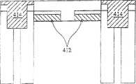
在一些例子中,形成一埋入隔离层可使用另一工艺。请参照图7A-7E,其说明提供一埋入隔离层的另一工艺。请参照图7A,形成第一外延层402(例如:一外延硅锗层)于衬底400上,衬底可为一半导体或一硅衬底。形成第二外延层404(例如:一外延硅层)于第一外延层402上。实施一图案化工艺以定义一缺口或本体接触的范围。在一例子中,沟槽电容工艺中形成的垫氧化及氮化层可作为一硬掩模。举例而言,可形成一垫层(pad layer),例如:一界面氧化硅层与氮化硅层的组合,于第二外延层404上。请参照图7B,垫层406可作为用于蚀刻部分的第一外延层402及第二外延层404以定义缺口区域408的一硬掩模。In some examples, another process may be used to form a buried isolation layer. Please refer to FIGS. 7A-7E , which illustrate another process for providing a buried isolation layer. Referring to FIG. 7A, a first epitaxial layer 402 (eg, an epitaxial silicon germanium layer) is formed on a
请参照图7C,垫层406将在图案化的步骤后被去除。然后,形成第三外延层410(例如:一外延硅层)在第二外延层404上与缺口区域408中。一般而言,于第一外延层402以上的外延材料厚度约为0.2~0.3μm。随后,另请参照图7D,沟槽电容形成于衬底400中,此沟槽电容例如包括图4G所示的第一电极110、介电层112、第二电极114、与导电插塞116,接着并形成浅沟槽414用以绝缘沟槽电容及暴露第一外延层402的一部分。在一些例子中,上述形成沟槽电容的工艺以及它的变化可被使用。Referring to FIG. 7C , the
请参照图7E,为了提供埋入隔离层,在一例子中,第一外延层在蚀刻形成浅沟槽414的工艺后被移除。因为第一外延层402与衬底400、第二外延层404材料的区别,而可选择性的移除第一外延层402,例如使用一湿蚀刻步骤。在移除步骤之后,可实施一热处理步骤,例如:一快速氧化法(rapidthermal oxidation,RTO)步骤,以在移除第一外延层402后所提供的空间形成衬层氧化物。在一些例子中,衬层氧化物的形成是藉由氧化部分的衬底400以及部分的第二外延层404。之后,一高密度等离子体氧化物填充于浅沟槽414中。因此,埋入隔离层412,例如:一埋入氧化硅层形成于一衬底区域中,该衬底区域包括:衬底400,第二外延层404,及第三外延层410提供的本体接触。Referring to FIG. 7E , in order to provide a buried isolation layer, in one example, the first epitaxial layer is removed after the etching process to form the
虽然本发明已揭露优选实施例如上,然其并非用以限定本发明,任何本领域内的技术人员,在不脱离本发明的精神和范围内,当可作些许的更动与润饰,因此本发明的保护范围以所附权利要求所界定者为准。Although the present invention has disclosed preferred embodiments as above, it is not intended to limit the present invention, and any skilled person in the art can make some changes and modifications without departing from the spirit and scope of the present invention. The scope of protection of the invention is defined by the appended claims.
Claims (22)
Applications Claiming Priority (2)
| Application Number | Priority Date | Filing Date | Title |
|---|---|---|---|
| US11/125,676 | 2005-05-10 | ||
| US11/125,676US7320912B2 (en) | 2005-05-10 | 2005-05-10 | Trench capacitors with buried isolation layer formed by an oxidation process and methods for manufacturing the same |
Publications (2)
| Publication Number | Publication Date |
|---|---|
| CN1862764A CN1862764A (en) | 2006-11-15 |
| CN100388419Ctrue CN100388419C (en) | 2008-05-14 |
Family
ID=37390147
Family Applications (1)
| Application Number | Title | Priority Date | Filing Date |
|---|---|---|---|
| CNB200510118408XAExpired - Fee RelatedCN100388419C (en) | 2005-05-10 | 2005-10-28 | Method for forming trench capacitor on substrate and trench capacitor |
Country Status (3)
| Country | Link |
|---|---|
| US (1) | US7320912B2 (en) |
| CN (1) | CN100388419C (en) |
| TW (1) | TWI284412B (en) |
Families Citing this family (2)
| Publication number | Priority date | Publication date | Assignee | Title |
|---|---|---|---|---|
| CN115346468A (en) | 2017-09-22 | 2022-11-15 | 索尼公司 | Display element, display device and electronic equipment |
| CN108231738A (en)* | 2017-12-29 | 2018-06-29 | 睿力集成电路有限公司 | Semiconductor device structure and its manufacturing method |
Citations (6)
| Publication number | Priority date | Publication date | Assignee | Title |
|---|---|---|---|---|
| JPH09232446A (en)* | 1996-02-20 | 1997-09-05 | Toshiba Corp | Semiconductor memory device and manufacturing method thereof |
| CN1218295A (en)* | 1997-09-30 | 1999-06-02 | 西门子公司 | Reduced parasitic leakage in semiconductor devices |
| US6756257B2 (en)* | 1999-07-16 | 2004-06-29 | International Business Machines Corporation | Patterned SOI regions on semiconductor chips |
| US6787837B2 (en)* | 2001-06-26 | 2004-09-07 | Kabushiki Kaisha Toshiba | Semiconductor memory with trench capacitor and method of manufacturing the same |
| WO2004102674A1 (en)* | 2003-05-13 | 2004-11-25 | Infineon Technologies Ag | Trench memory capacitor and method for producing the same |
| US20050093066A1 (en)* | 2001-12-27 | 2005-05-05 | Hajime Nagano | Semiconductor device using partial SOI substrate and manufacturing method thereof |
Family Cites Families (4)
| Publication number | Priority date | Publication date | Assignee | Title |
|---|---|---|---|---|
| US5508219A (en)* | 1995-06-05 | 1996-04-16 | International Business Machines Corporation | SOI DRAM with field-shield isolation and body contact |
| US5770484A (en)* | 1996-12-13 | 1998-06-23 | International Business Machines Corporation | Method of making silicon on insulator buried plate trench capacitor |
| US6974991B2 (en)* | 2003-10-29 | 2005-12-13 | International Business Machines Corp. | DRAM cell with buried collar and self-aligned buried strap |
| US20060105519A1 (en)* | 2004-11-17 | 2006-05-18 | Infineon Technologies Richmond, L.P | DRAM on SOI |
- 2005
- 2005-05-10USUS11/125,676patent/US7320912B2/enactiveActive
- 2005-09-29TWTW094133961Apatent/TWI284412B/ennot_activeIP Right Cessation
- 2005-10-28CNCNB200510118408XApatent/CN100388419C/ennot_activeExpired - Fee Related
Patent Citations (6)
| Publication number | Priority date | Publication date | Assignee | Title |
|---|---|---|---|---|
| JPH09232446A (en)* | 1996-02-20 | 1997-09-05 | Toshiba Corp | Semiconductor memory device and manufacturing method thereof |
| CN1218295A (en)* | 1997-09-30 | 1999-06-02 | 西门子公司 | Reduced parasitic leakage in semiconductor devices |
| US6756257B2 (en)* | 1999-07-16 | 2004-06-29 | International Business Machines Corporation | Patterned SOI regions on semiconductor chips |
| US6787837B2 (en)* | 2001-06-26 | 2004-09-07 | Kabushiki Kaisha Toshiba | Semiconductor memory with trench capacitor and method of manufacturing the same |
| US20050093066A1 (en)* | 2001-12-27 | 2005-05-05 | Hajime Nagano | Semiconductor device using partial SOI substrate and manufacturing method thereof |
| WO2004102674A1 (en)* | 2003-05-13 | 2004-11-25 | Infineon Technologies Ag | Trench memory capacitor and method for producing the same |
Also Published As
| Publication number | Publication date |
|---|---|
| US7320912B2 (en) | 2008-01-22 |
| CN1862764A (en) | 2006-11-15 |
| US20060255388A1 (en) | 2006-11-16 |
| TWI284412B (en) | 2007-07-21 |
| TW200640000A (en) | 2006-11-16 |
Similar Documents
| Publication | Publication Date | Title |
|---|---|---|
| US6437401B1 (en) | Structure and method for improved isolation in trench storage cells | |
| KR100403066B1 (en) | Improved vertical mosfet | |
| US6150210A (en) | Memory cell that includes a vertical transistor and a trench capacitor | |
| KR100560647B1 (en) | Reduced parasitic leakage in semiconductor devices | |
| US7557410B2 (en) | Dynamic random access memory device | |
| KR19990044767A (en) | Semiconductor devices | |
| GB2341724A (en) | Method for fabricating a high-density semiconductor memory device | |
| US7633117B2 (en) | Capacitorless DRAM with cylindrical auxiliary gate and fabrication method thereof | |
| JPH04233272A (en) | Dluble-trench semiconductor memory structure and its manufacture | |
| US6479852B1 (en) | Memory cell having a deep trench capacitor and a vertical channel | |
| US6414347B1 (en) | Vertical MOSFET | |
| KR100979362B1 (en) | Semiconductor device and manufacturing method thereof | |
| US7250650B2 (en) | Field-effect transistor structure and associated semiconductor memory cell | |
| JP5132120B2 (en) | GAIN CELL AND METHOD FOR MANUFACTURING AND USING THE SAME | |
| KR100517219B1 (en) | Dram cell arrangement with dynamic gain memory cells, and method for the production thereof | |
| CN100388419C (en) | Method for forming trench capacitor on substrate and trench capacitor | |
| US7135735B2 (en) | Semiconductor device | |
| JPH11135752A (en) | Semiconductor memory device and method of manufacturing the same | |
| US7332390B2 (en) | Semiconductor memory device and fabrication thereof | |
| JP2003078033A (en) | Semiconductor device and manufacturing method therefor | |
| US8349719B2 (en) | Semiconductor device and method for fabricating the same | |
| JP4348299B2 (en) | Field effect transistor structure, related semiconductor memory cell, and related manufacturing method | |
| JP2000323652A (en) | Semiconductor device and manufacture thereof | |
| HK1009207A (en) | Memory cell that includes a vertical transistor and a trench capacitor |
Legal Events
| Date | Code | Title | Description |
|---|---|---|---|
| C06 | Publication | ||
| PB01 | Publication | ||
| C10 | Entry into substantive examination | ||
| SE01 | Entry into force of request for substantive examination | ||
| C14 | Grant of patent or utility model | ||
| GR01 | Patent grant | ||
| C17 | Cessation of patent right | ||
| CF01 | Termination of patent right due to non-payment of annual fee | Granted publication date:20080514 Termination date:20091130 |