CN100386797C - A Line and Field Signal Generation Method Facilitating Realization of Digital Video Image Scaling and Interpolation - Google Patents
A Line and Field Signal Generation Method Facilitating Realization of Digital Video Image Scaling and InterpolationDownload PDFInfo
- Publication number
- CN100386797C CN100386797CCNB2005100962939ACN200510096293ACN100386797CCN 100386797 CCN100386797 CCN 100386797CCN B2005100962939 ACNB2005100962939 ACN B2005100962939ACN 200510096293 ACN200510096293 ACN 200510096293ACN 100386797 CCN100386797 CCN 100386797C
- Authority
- CN
- China
- Prior art keywords
- line
- signal
- field
- synchronization
- output
- Prior art date
- Legal status (The legal status is an assumption and is not a legal conclusion. Google has not performed a legal analysis and makes no representation as to the accuracy of the status listed.)
- Expired - Fee Related
Links
- 238000000034methodMethods0.000titleclaimsabstractdescription27
- 230000007274generation of a signal involved in cell-cell signalingEffects0.000titleclaimsabstractdescription16
- 230000001186cumulative effectEffects0.000claimsabstractdescription6
- 230000009286beneficial effectEffects0.000claimsabstractdescription5
- 230000007704transitionEffects0.000claimsdescription5
- 230000008569processEffects0.000claimsdescription3
- 230000001360synchronised effectEffects0.000claimsdescription3
- 230000000694effectsEffects0.000claimsdescription2
- 239000000872bufferSubstances0.000abstract1
- 238000004364calculation methodMethods0.000description7
- 238000010586diagramMethods0.000description5
- 238000009825accumulationMethods0.000description2
- 238000005516engineering processMethods0.000description2
- 230000009471actionEffects0.000description1
- 230000008901benefitEffects0.000description1
- 230000005540biological transmissionEffects0.000description1
- 238000009125cardiac resynchronization therapyMethods0.000description1
- 238000006243chemical reactionMethods0.000description1
- 230000003111delayed effectEffects0.000description1
- 230000006870functionEffects0.000description1
- 238000004519manufacturing processMethods0.000description1
- 230000000737periodic effectEffects0.000description1
Images


Landscapes
- Controls And Circuits For Display Device (AREA)
- Television Systems (AREA)
Abstract
Translated fromChinese
Description
Translated fromChinese技术领域technical field
本发明属于数字视频图像处理与显示技术领域,具体涉及一种利于实现数字视频图像缩放插值的行场信号产生方法。The invention belongs to the technical field of digital video image processing and display, and in particular relates to a method for generating line and field signals which is beneficial to realizing scaling and interpolation of digital video images.
背景技术Background technique
数字视频图像缩放芯片(Scaler)是平板显示器件不可或缺的一部分,实现图像分辨率转换的功能,而图像缩放插值算法是数字视频图像缩放芯片的核心算法。The digital video image scaling chip (Scaler) is an indispensable part of the flat panel display device, which realizes the function of image resolution conversion, and the image scaling interpolation algorithm is the core algorithm of the digital video image scaling chip.
图像缩放插值算法常用的有最近邻插值、双线性插值和双三次插值,其中双三次插值的效果最好,但计算量和硬件实现复杂度要比前两种算法大得多。Commonly used image scaling interpolation algorithms are nearest neighbor interpolation, bilinear interpolation and bicubic interpolation, among which bicubic interpolation has the best effect, but the amount of calculation and hardware implementation complexity are much larger than the former two algorithms.
而图1是一种节省硬件资源的实现一维方向上双三次插值的装置,支持和实现该装置的关键之一就是输出行场信号的产生方法。Figure 1 is a device that saves hardware resources and realizes bicubic interpolation in the one-dimensional direction. One of the keys to supporting and realizing this device is the method for generating the output line and field signals.
在上述的实现一维方向上双三次插值的装置中,由输入行场信号控制数据写入存储器(行存储器如寄存器组或点存储器如fifo),由输出行场信号控制当前插值点周围4邻域内的4个点数据从存储器中读出送入插值计算模块,经计算后输出数据完成双三次插值过程。该装置的优点在于数据存储器前后无需fifo缓存,节省硬件资源,且读写控制逻辑简单。但这就要求数据存储器的写入和读出要保持一定的同步性,即不能有写入赶超或滞后读出的情况发生。同时,该装置也可实现双线性插值和最近邻插值。In the above-mentioned device for realizing bicubic interpolation in the one-dimensional direction, the input line and field signals control data writing into the memory (line memory such as register bank or point memory such as fifo), and the output line and field signals control the four neighbors around the current interpolation point The data of 4 points in the domain is read from the memory and sent to the interpolation calculation module, and the output data after calculation completes the bicubic interpolation process. The advantage of the device is that no fifo cache is needed before and after the data memory, hardware resources are saved, and the read and write control logic is simple. However, this requires that the writing and reading of the data memory must maintain a certain degree of synchronization, that is, there must be no writing catch-up or delayed reading. At the same time, the device can also realize bilinear interpolation and nearest neighbor interpolation.
为实现该装置,对输出行场信号的要求为:In order to realize the device, the requirements for the output line and field signals are:
1、保证输出行场信号的周期性。虽然平板显示器件对视频信号行场的周期性的要求不像CRT那么严格,但是不同厂商生产的面板对输入行场有着不同的要求,无疑输出标准的周期性行场信号将具有通用性。1. Ensure the periodicity of the output line and field signals. Although flat panel display devices are not as strict as CRTs on the periodicity of video signal lines, panels produced by different manufacturers have different requirements for input line fields. Undoubtedly, outputting standard periodic line field signals will be universal.
2、保证输入、输出行场信号的同步性,即满足数据存储器的读写操作的同步性,不会发生读写超赶,保证当前插值点运算所需的4领域像素值存在于数据存储器中并且能够在输出行场信号的控制下读出。2. Guarantee the synchronization of the input and output line and field signals, that is, to meet the synchronization of the read and write operations of the data memory, and there will be no overtaking of reading and writing, and ensure that the pixel values of the 4 fields required for the current interpolation point calculation exist in the data memory And it can be read out under the control of the output row and field signals.
发明内容Contents of the invention
针对背景技术中提出的图像插值实现装置中行场信号产生问题,本发明的目的在于,提出一种利于实现数字视频图像缩放插值的行场信号产生方法。该方法可以满足(1)保证输出行场信号的周期性(2)保证输入、输出行场信号的同步性这两点要求,有利于实现背景技术中提到的节省硬件资源的图像插值实现装置。Aiming at the problem of line and field signal generation in the image interpolation implementation device proposed in the background art, the purpose of the present invention is to propose a line and field signal generation method that is beneficial to realize scaling and interpolation of digital video images. The method can meet the two requirements of (1) ensuring the periodicity of the output line and field signals (2) ensuring the synchronization of the input and output line and field signals, and is conducive to the realization of the image interpolation implementation device that saves hardware resources mentioned in the background technology .
为了实现上述目的,本发明的技术方案,一种利于实现数字视频图像缩放插值的行场信号产生方法,其特征在于,该方法在一维方向上双三次插值的装置中采用输入行场信号调制输出行场信号,保证两者的同步性,并且累加计数的一个循环长度限制在63行以内,缩小累加误差,满足输出行场信号的周期性要求。该方法详述如下:In order to achieve the above object, the technical solution of the present invention is a method for generating line and field signals that is conducive to realizing digital video image scaling and interpolation, which is characterized in that the method adopts input line and field signal modulation Output the line and field signals to ensure the synchronization of the two, and the length of a cycle of accumulated counting is limited to 63 lines, reducing the accumulation error and meeting the periodicity requirements of the output line and field signals. The method is detailed as follows:
1、输入、输出行场信号的同步性和周期性1. Synchronization and periodicity of input and output line and field signals
背景技术中提出的图像插值实现装置中数据需经过存储器是因为缩放前后会发生时钟域的变化,即点频改变;但因未用到片外SDRAM,所以无法实现视频信号的场频改变,也就是输入、输出场同步及有效信号的周期不变,而数据写入存储器需要等待3行的时间后才能开始读出所需数据进行插值计算,因此输入、输出场有效信号之间要相差输入3行的时间延迟。而缩放前后每场内的行数,即输入、输出行同步头的个数之比等于缩放比例因子,也就是说如果缩放比例因子为m/n,那么每输入m行的时间内,输出n行,输入行同步及有效信号m行的时间跟输出行同步及有效信号n行的时间相等。The data in the image interpolation implementation device proposed in the background technology needs to pass through the memory because the clock domain changes before and after zooming, that is, the point frequency changes; but because the off-chip SDRAM is not used, the field frequency of the video signal cannot be changed, and the field frequency of the video signal cannot be changed. That is, the period of the input and output field synchronization and effective signals remains unchanged, and the data is written into the memory to wait for 3 lines before starting to read the required data for interpolation calculations, so the difference between the input and output field effective signals must be 3 Row time delay. The number of lines in each field before and after scaling, that is, the ratio of the number of input and output line synchronization heads is equal to the scaling factor, that is, if the scaling factor is m/n, then every time m lines are input, n is output line, the time of input line synchronization and valid signal m lines is equal to the time of output line synchronization and valid signal n lines.
输入、输出行场信号的同步性就是要满足上述的(1)输入、输出的场同步及有效信号的周期不变且有效信号相差输入3行的时间延迟,(2)输入行同步及有效信号m行的时间跟输出行同步及有效信号n行的时间相等这两个条件。The synchronization of the input and output line and field signals is to meet the above (1) The input and output field synchronization and the period of the effective signal are unchanged and the effective signal is different from the time delay of the
输入、输出行场信号的周期性就是行场同步及有效信号的每行的象素点数保持一致,但是平板显示器件可以容忍一定程度的误差。The periodicity of the input and output line and field signals means that the line and field synchronization and the number of pixels in each line of the effective signal are consistent, but the flat panel display device can tolerate a certain degree of error.
2、行同步和有效信号的产生方法原理2. The principle of line synchronization and effective signal generation method
设缩放比例因子为m/n,为了便于硬件实现,要求该比例因子为最简质数比,并且m,n<64(若降低精度要求也可为32);另设输入、输出的每行传输时间,即行同步信号周期分别为hperiod_in和hperiod_out,输入每行总象素点数为htotal_in,输入时钟周期Tclk,则根据上述同步性的条件(2),他们的关系为:Set the scaling factor as m/n. For the convenience of hardware implementation, the scaling factor is required to be the simplest prime number ratio, and m, n<64 (it can also be 32 if the precision requirement is lowered); additionally, each line of input and output is transmitted Time, that is, the period of the line synchronization signal is hperiod_in and hperiod_out respectively, the total number of pixels in each line is htotal_in, and the input clock cycle is Tclk. According to the above synchronization condition (2), their relationship is:
由上式得出,输入每
同时,上述操作的一个循环长度等于m,即每输入m行即清零重新开始新一轮计数循环,这样把累加计数误差限制在每个循环的最后一行,也就是输出每n行的最后一行的象素点数或多或少有些误差,但是这个误差对于平板显示器件是可以接受的,能够正常显示,因此满足了周期性要求。At the same time, the length of a cycle of the above operation is equal to m, that is, every input of m lines is cleared and a new round of counting cycle is restarted, so that the cumulative counting error is limited to the last line of each cycle, that is, the last line of output every n lines There are more or less errors in the number of pixels, but this error is acceptable for flat panel display devices and can be displayed normally, so it meets the periodicity requirements.
3、场同步及有效信号产生方法原理3. Principle of field synchronization and effective signal generation method
由输入场同步头的下降沿脉冲作为清零信号,对已产生的输出行同步信号进行行计数,通过设置高电平(或低电平)起始和结束位置,并考虑到输出场有效信号要滞后输入场有效信号3行输入的时间,即可产生输出场同步及有效信号,且满足同步性。The falling edge pulse of the input field sync head is used as a clear signal to count the lines of the generated output line sync signal, by setting the high level (or low level) start and end positions, and taking into account the output field valid signal To lag the input time of the effective signal of the input field by 3 lines, the output field synchronous and effective signals can be generated, and the synchronism is satisfied.
由于输出行同步及有效信号已满足平板显示器件的周期性要求,在此基础上产生的场同步及有效信号同时由输入场同步信号调制,足以满足周期性要求。Since the output line synchronization and effective signals have met the periodicity requirements of flat panel display devices, the field synchronization and effective signals generated on this basis are simultaneously modulated by the input field synchronization signals, which is sufficient to meet the periodicity requirements.
本发明的行场信号产生方法有利于实现背景技术中所提到的图像插值实现装置,使得该装置数据存储器前后无需fifo缓存,节省硬件资源,且读写控制逻辑简单。本发明的方法用输入行场信号调制输出行场信号,满足了该装置所要求的输出行场信号的同步性,使得当前插值点运算所需的4领域像素值存在于数据存储器中并且能够在输出行场信号的控制下读出;另外累加计数的一个循环长度限制在63行以内,缩小累加误差,从而输出行场信号的周期性满足该装置的要求,使得缩放后的视频信号能够在平板显示器件上正常显示。The line and field signal generation method of the present invention is beneficial to realize the image interpolation implementation device mentioned in the background art, so that the data memory of the device does not need fifo cache before and after, saving hardware resources, and the read and write control logic is simple. The method of the present invention uses the input line and field signal to modulate the output line and field signal, which meets the synchronization of the output line and field signal required by the device, so that the 4-field pixel values required for the current interpolation point calculation exist in the data memory and can be stored in the data memory. Read out under the control of the output line and field signals; in addition, the cumulative counting cycle length is limited within 63 lines to reduce the accumulation error, so that the periodicity of the output line and field signals meets the requirements of the device, so that the scaled video signal can be displayed on the flat panel Normal display on the display device.
附图说明Description of drawings
图1是一维方向上双三次插值的装置结构图;Fig. 1 is a device structure diagram of bicubic interpolation in one-dimensional direction;
图2是本发明行场信号产生方法示意图;Fig. 2 is a schematic diagram of the method for producing line and field signals of the present invention;
图3是行同步及有效信号产生方法示意图;Fig. 3 is a schematic diagram of line synchronization and effective signal generation method;
图4是场同步及有效信号产生方法示意图;Fig. 4 is a schematic diagram of field synchronization and effective signal generation method;
图5是输出行计数状态机状态转换图;Fig. 5 is a state transition diagram of the output line counting state machine;
下面结合附图对本发明进行进一步的详细说明。The present invention will be further described in detail below in conjunction with the accompanying drawings.
具体实施方式Detailed ways
参见图2,本发明的行场信号产生方法通过输入行场信号来调制产生输出行场信号,同时需要缩放比例因子及其他参数如hnum_trans等参与计算。下面结合图3和图4详细描述。Referring to FIG. 2 , the method for generating line and field signals of the present invention modulates input line and field signals to generate output line and field signals, and requires scaling factors and other parameters such as hnum_trans to participate in the calculation. The following describes in detail with reference to FIG. 3 and FIG. 4 .
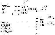
参见图3,本发明行同步及有效信号产生方法包括:触发信号生成模块1、输入行数计数模块2、输入时钟计数模块3、输出时钟计数模块4,详述如下:Referring to Fig. 3, the line synchronization and effective signal generation method of the present invention comprises: trigger
1、触发信号生成模块1. Trigger signal generation module
触发信号trigger由系统复位信号(低有效)复位后的第一个输入场同步头下降沿开始有效,所有操作均在此后进行,保证输入场同步信号对输出行场信号的调制作用,以满足同步性。The trigger signal trigger is effective from the falling edge of the first input field sync head after the system reset signal (low active) is reset, and all operations are performed thereafter to ensure the modulation of the input field sync signal to the output line field signal to meet the synchronization sex.
2、输入行数计数模块2. Input line number counting module
通过对输入行同步头计数,每三个行同步头的下降沿产生一个脉冲,生成循环计数清零信号loop_clr,每输入m行强制清零开始新一轮计数循环操作。这样,累加计数误差就限制在输出每n行的最后一行,使输出行场信号的周期性满足平板显示器件的要求。By counting the input line sync heads, a pulse is generated every three falling edges of the line sync heads, and a loop count clear signal loop_clr is generated, and a new round of count cycle operation is started by forced clearing every m lines input. In this way, the accumulative counting error is limited to the last line of every n lines, so that the periodicity of the output line and field signals meets the requirements of the flat panel display device.
3、输入时钟计数模块3. Input clock counting module
通过在输入时钟域内对象素点计数,每计数hnum_trans即产生一个脉冲,生成输出行同步计数清零信号ohs_clr。需要注意的是计数在遇到loop_clr脉冲时强制清零。By counting the pixel points in the input clock domain, a pulse is generated for each count hnum_trans, and the output line synchronous count clear signal ohs_clr is generated. It should be noted that the count is forced to be cleared when it encounters a loop_clr pulse.
4、输出时钟计数模块4. Output clock counting module
通过在输出时钟域内对象素点计数,在ohs_clr的脉冲作用下清零,根据行同步及有效信号低电平开始及结束参数值ohs_st,ohs_end,ohref_st,ohref_end值生成行同步信号ohs及行有效信号ohref。By counting the pixel points in the output clock domain, clearing under the pulse of ohs_clr, and generating the line synchronization signal ohs and the line valid signal according to the line synchronization and valid signal low level start and end parameter values ohs_st, ohs_end, ohref_st, ohref_end values oh ref.
参见图3,本发明场同步及有效信号产生方法包括:输出行计数状态机模块5、输出行数计数模块6,详述如下:Referring to Fig. 3, the field synchronization of the present invention and valid signal generation method comprise: output line counting
5、输出行计数状态机模块5. Output line counting state machine module
参见图4,该状态机在状态转换每场为一个循环,一场内其状态跳变过程为state0→state1→state2→state0,到下一个场同步头下降沿之前,保持在state0不再跳变,避免了不必要的翻转,节省功耗。See Figure 4. The state transition of the state machine is a cycle per field, and the state transition process in one field is state0→state1→state2→state0, and it remains at state0 before the falling edge of the next field synchronization header. , to avoid unnecessary flipping and save power consumption.
若当前状态(current state)为state2时,在行同步头的下降沿产生一个脉冲,产生输出场同步计数清零信号ovs_clr。If the current state (current state) is state2, a pulse is generated on the falling edge of the line sync head, and the output field sync count clear signal ovs_clr is generated.
需要注意的是所有操作均在trigger信号有效时进行。It should be noted that all operations are performed when the trigger signal is valid.
6、输出行数计数模块6. Output row number counting module
在输出时钟域内,对输出行同步头计数,在ovs_clr的脉冲作用下清零,根据场同步及有效信号低电平开始及结束参数值ovs_st,ovs_end,ovblk_st,ovblk_end值生成行同步信号ovs及行有效信号ovblk,特别的,ovblk_st和ovblk_end的值要保证输出场有效ovblk信号满足与输入场有效信号相差输入3行时间延迟的要求。In the output clock domain, count the output line synchronization head, clear it under the pulse of ovs_clr, and generate line synchronization signal ovs and line The effective signal ovblk, especially, the values of ovblk_st and ovblk_end should ensure that the effective ovblk signal in the output field meets the requirement of input 3-line time delay from the effective signal in the input field.
Claims (1)
Translated fromChinesePriority Applications (1)
| Application Number | Priority Date | Filing Date | Title |
|---|---|---|---|
| CNB2005100962939ACN100386797C (en) | 2005-11-03 | 2005-11-03 | A Line and Field Signal Generation Method Facilitating Realization of Digital Video Image Scaling and Interpolation |
Applications Claiming Priority (1)
| Application Number | Priority Date | Filing Date | Title |
|---|---|---|---|
| CNB2005100962939ACN100386797C (en) | 2005-11-03 | 2005-11-03 | A Line and Field Signal Generation Method Facilitating Realization of Digital Video Image Scaling and Interpolation |
Publications (2)
| Publication Number | Publication Date |
|---|---|
| CN1794343A CN1794343A (en) | 2006-06-28 |
| CN100386797Ctrue CN100386797C (en) | 2008-05-07 |
Family
ID=36805739
Family Applications (1)
| Application Number | Title | Priority Date | Filing Date |
|---|---|---|---|
| CNB2005100962939AExpired - Fee RelatedCN100386797C (en) | 2005-11-03 | 2005-11-03 | A Line and Field Signal Generation Method Facilitating Realization of Digital Video Image Scaling and Interpolation |
Country Status (1)
| Country | Link |
|---|---|
| CN (1) | CN100386797C (en) |
Families Citing this family (3)
| Publication number | Priority date | Publication date | Assignee | Title |
|---|---|---|---|---|
| CN101662598B (en)* | 2008-08-26 | 2013-04-24 | 深圳艾科创新微电子有限公司 | Scaling system for continuous video data stream |
| CN101686392B (en)* | 2008-09-24 | 2011-06-08 | 安凯(广州)微电子技术有限公司 | Image interpolation method, mobile multimedia processor and multimedia player terminal |
| CN108231039B (en)* | 2018-01-29 | 2021-02-09 | 京东方科技集团股份有限公司 | FPGA-based frame start bit dynamic capturing method and device |
Citations (5)
| Publication number | Priority date | Publication date | Assignee | Title |
|---|---|---|---|---|
| CN1125030A (en)* | 1993-06-01 | 1996-06-19 | 汤姆森多媒体公司 | Method and device for motion compensation interpolation |
| US5534934A (en)* | 1993-06-18 | 1996-07-09 | Hitachi, Ltd. | Television receiver capable of enlarging and compressing image |
| JP2001086368A (en)* | 1999-09-09 | 2001-03-30 | Dainippon Screen Mfg Co Ltd | Image processor |
| CN1516458A (en)* | 2003-08-28 | 2004-07-28 | 上海交通大学 | Control Method of Video Format Converter Using Two-Dimensional Multi-Phase Interpolation Filtering |
| CN1663258A (en)* | 2002-06-28 | 2005-08-31 | 杜比实验室认证公司 | Improved video compression frame interpolation |
- 2005
- 2005-11-03CNCNB2005100962939Apatent/CN100386797C/ennot_activeExpired - Fee Related
Patent Citations (5)
| Publication number | Priority date | Publication date | Assignee | Title |
|---|---|---|---|---|
| CN1125030A (en)* | 1993-06-01 | 1996-06-19 | 汤姆森多媒体公司 | Method and device for motion compensation interpolation |
| US5534934A (en)* | 1993-06-18 | 1996-07-09 | Hitachi, Ltd. | Television receiver capable of enlarging and compressing image |
| JP2001086368A (en)* | 1999-09-09 | 2001-03-30 | Dainippon Screen Mfg Co Ltd | Image processor |
| CN1663258A (en)* | 2002-06-28 | 2005-08-31 | 杜比实验室认证公司 | Improved video compression frame interpolation |
| CN1516458A (en)* | 2003-08-28 | 2004-07-28 | 上海交通大学 | Control Method of Video Format Converter Using Two-Dimensional Multi-Phase Interpolation Filtering |
Non-Patent Citations (2)
| Title |
|---|
| 一种自适应最大相关性数字图像插值算法. 陈建辉,王博亮,徐中佑,张砚臣.厦门大学学报(自然科学版),第44卷第3期. 2003* |
| 数字高速视频图像的解码算法. 黄占华,蔡怀宇,张昊等.光电工程,第31卷第5期. 2004* |
Also Published As
| Publication number | Publication date |
|---|---|
| CN1794343A (en) | 2006-06-28 |
Similar Documents
| Publication | Publication Date | Title |
|---|---|---|
| CN107249101B (en) | High-resolution image acquisition and processing device | |
| CN103702060B (en) | Definition display device and video signal conversion method | |
| CN103248797A (en) | Video resolution enhancing method and module based on FPGA (field programmable gate array) | |
| CN103065598A (en) | Control method for preventing liquid crystal display from being blurred | |
| WO2014101642A1 (en) | Video playing apparatus and method | |
| CN118521458A (en) | Image generation and display method and system based on FPGA | |
| CN100455002C (en) | A digital video image scaling method and circuit based on bicubic interpolation | |
| CN104469241B (en) | A kind of device for realizing video frame rate conversion | |
| CN100386797C (en) | A Line and Field Signal Generation Method Facilitating Realization of Digital Video Image Scaling and Interpolation | |
| CN114125182A (en) | A method for realizing 4K high-definition display based on FPGA | |
| CN115037885A (en) | Image enlarging method, device, equipment, medium and display for liquid crystal screen | |
| KR100938338B1 (en) | Semiconductor device and buffer control circuit | |
| CN101662598B (en) | Scaling system for continuous video data stream | |
| CN111199515B (en) | Scaler, image scaling method and device | |
| US7349032B2 (en) | Circuit to resize and enlarge an image signal and resizing and enlargement method for an image signal | |
| CN113141481A (en) | Video time sequence conversion method and device and computer readable medium | |
| JP4708528B2 (en) | Video signal converter | |
| CN101777298B (en) | Data drive circuit with block mode and block window pixel data processing method | |
| CN104270585A (en) | CMOS image sensor data read and write control method | |
| CN100361193C (en) | Display device, picture adjusting method thereof and video wall with display device | |
| JP2002014645A (en) | Image data conversion device for in-frame time division gray scale display system | |
| US8085345B2 (en) | Image processing apparatus and image processing method | |
| CN101727655B (en) | Image zooming method and device thereof | |
| CN112714264A (en) | FPGA-based HDM-to-eDP interface conversion device and interface conversion method | |
| CN118714247A (en) | Low-latency digital and analog dual-channel synchronous display method and system |
Legal Events
| Date | Code | Title | Description |
|---|---|---|---|
| C06 | Publication | ||
| PB01 | Publication | ||
| C10 | Entry into substantive examination | ||
| SE01 | Entry into force of request for substantive examination | ||
| C14 | Grant of patent or utility model | ||
| GR01 | Patent grant | ||
| C17 | Cessation of patent right | ||
| CF01 | Termination of patent right due to non-payment of annual fee | Granted publication date:20080507 Termination date:20131103 |