CN100378902C - Thin film transistor array panel and method of manufacturing the same - Google Patents
Thin film transistor array panel and method of manufacturing the sameDownload PDFInfo
- Publication number
- CN100378902C CN100378902CCNB031514987ACN03151498ACN100378902CCN 100378902 CCN100378902 CCN 100378902CCN B031514987 ACNB031514987 ACN B031514987ACN 03151498 ACN03151498 ACN 03151498ACN 100378902 CCN100378902 CCN 100378902C
- Authority
- CN
- China
- Prior art keywords
- layer
- conductive layer
- transistor array
- film transistor
- contact
- Prior art date
- Legal status (The legal status is an assumption and is not a legal conclusion. Google has not performed a legal analysis and makes no representation as to the accuracy of the status listed.)
- Expired - Fee Related
Links
Images


Classifications
- H—ELECTRICITY
- H10—SEMICONDUCTOR DEVICES; ELECTRIC SOLID-STATE DEVICES NOT OTHERWISE PROVIDED FOR
- H10D—INORGANIC ELECTRIC SEMICONDUCTOR DEVICES
- H10D30/00—Field-effect transistors [FET]
- H10D30/60—Insulated-gate field-effect transistors [IGFET]
- H10D30/67—Thin-film transistors [TFT]
- H10D30/6729—Thin-film transistors [TFT] characterised by the electrodes
- H10D30/6737—Thin-film transistors [TFT] characterised by the electrodes characterised by the electrode materials
- H—ELECTRICITY
- H10—SEMICONDUCTOR DEVICES; ELECTRIC SOLID-STATE DEVICES NOT OTHERWISE PROVIDED FOR
- H10D—INORGANIC ELECTRIC SEMICONDUCTOR DEVICES
- H10D30/00—Field-effect transistors [FET]
- H10D30/60—Insulated-gate field-effect transistors [IGFET]
- H10D30/67—Thin-film transistors [TFT]
- H10D30/6729—Thin-film transistors [TFT] characterised by the electrodes
- H—ELECTRICITY
- H10—SEMICONDUCTOR DEVICES; ELECTRIC SOLID-STATE DEVICES NOT OTHERWISE PROVIDED FOR
- H10D—INORGANIC ELECTRIC SEMICONDUCTOR DEVICES
- H10D30/00—Field-effect transistors [FET]
- H10D30/60—Insulated-gate field-effect transistors [IGFET]
- H10D30/67—Thin-film transistors [TFT]
- H10D30/674—Thin-film transistors [TFT] characterised by the active materials
- H10D30/6741—Group IV materials, e.g. germanium or silicon carbide
- H10D30/6743—Silicon
- H—ELECTRICITY
- H10—SEMICONDUCTOR DEVICES; ELECTRIC SOLID-STATE DEVICES NOT OTHERWISE PROVIDED FOR
- H10D—INORGANIC ELECTRIC SEMICONDUCTOR DEVICES
- H10D86/00—Integrated devices formed in or on insulating or conducting substrates, e.g. formed in silicon-on-insulator [SOI] substrates or on stainless steel or glass substrates
- H10D86/01—Manufacture or treatment
- H10D86/021—Manufacture or treatment of multiple TFTs
- H10D86/0231—Manufacture or treatment of multiple TFTs using masks, e.g. half-tone masks
- H—ELECTRICITY
- H10—SEMICONDUCTOR DEVICES; ELECTRIC SOLID-STATE DEVICES NOT OTHERWISE PROVIDED FOR
- H10D—INORGANIC ELECTRIC SEMICONDUCTOR DEVICES
- H10D86/00—Integrated devices formed in or on insulating or conducting substrates, e.g. formed in silicon-on-insulator [SOI] substrates or on stainless steel or glass substrates
- H10D86/40—Integrated devices formed in or on insulating or conducting substrates, e.g. formed in silicon-on-insulator [SOI] substrates or on stainless steel or glass substrates characterised by multiple TFTs
- H10D86/441—Interconnections, e.g. scanning lines
- H—ELECTRICITY
- H10—SEMICONDUCTOR DEVICES; ELECTRIC SOLID-STATE DEVICES NOT OTHERWISE PROVIDED FOR
- H10D—INORGANIC ELECTRIC SEMICONDUCTOR DEVICES
- H10D86/00—Integrated devices formed in or on insulating or conducting substrates, e.g. formed in silicon-on-insulator [SOI] substrates or on stainless steel or glass substrates
- H10D86/40—Integrated devices formed in or on insulating or conducting substrates, e.g. formed in silicon-on-insulator [SOI] substrates or on stainless steel or glass substrates characterised by multiple TFTs
- H10D86/60—Integrated devices formed in or on insulating or conducting substrates, e.g. formed in silicon-on-insulator [SOI] substrates or on stainless steel or glass substrates characterised by multiple TFTs wherein the TFTs are in active matrices
- H—ELECTRICITY
- H10—SEMICONDUCTOR DEVICES; ELECTRIC SOLID-STATE DEVICES NOT OTHERWISE PROVIDED FOR
- H10D—INORGANIC ELECTRIC SEMICONDUCTOR DEVICES
- H10D30/00—Field-effect transistors [FET]
- H10D30/01—Manufacture or treatment
- H10D30/021—Manufacture or treatment of FETs having insulated gates [IGFET]
- H10D30/031—Manufacture or treatment of FETs having insulated gates [IGFET] of thin-film transistors [TFT]
- H10D30/0312—Manufacture or treatment of FETs having insulated gates [IGFET] of thin-film transistors [TFT] characterised by the gate electrodes
- H10D30/0316—Manufacture or treatment of FETs having insulated gates [IGFET] of thin-film transistors [TFT] characterised by the gate electrodes of lateral bottom-gate TFTs comprising only a single gate
- H—ELECTRICITY
- H10—SEMICONDUCTOR DEVICES; ELECTRIC SOLID-STATE DEVICES NOT OTHERWISE PROVIDED FOR
- H10D—INORGANIC ELECTRIC SEMICONDUCTOR DEVICES
- H10D30/00—Field-effect transistors [FET]
- H10D30/01—Manufacture or treatment
- H10D30/021—Manufacture or treatment of FETs having insulated gates [IGFET]
- H10D30/031—Manufacture or treatment of FETs having insulated gates [IGFET] of thin-film transistors [TFT]
- H10D30/0321—Manufacture or treatment of FETs having insulated gates [IGFET] of thin-film transistors [TFT] comprising silicon, e.g. amorphous silicon or polysilicon
Landscapes
- Liquid Crystal (AREA)
- Thin Film Transistor (AREA)
Abstract
Description
Translated fromChinese技术领域technical field
本发明涉及薄膜晶体管阵列板及其制造方法,特别涉及用于液晶显示器的薄膜晶体管阵列板及其制造方法。The invention relates to a thin film transistor array board and a manufacturing method thereof, in particular to a thin film transistor array board used for a liquid crystal display and a manufacturing method thereof.
背景技术Background technique
液晶显示器(LCD)是最广泛使用的平板显示器之一。液晶显示器包括设置有场发生电极的两块基板和夹在两块基板之间的液晶层(LC)。液晶显示器通过给场发生电极加电压在液晶层中产生电场来显示图像,该电场确定液晶层中的液晶分子取向以调节入射光的偏振。Liquid crystal displays (LCDs) are among the most widely used flat panel displays. A liquid crystal display includes two substrates provided with field generating electrodes and a liquid crystal layer (LC) sandwiched between the two substrates. The liquid crystal display displays images by applying voltage to the field generating electrodes to generate an electric field in the liquid crystal layer, and the electric field determines the orientation of liquid crystal molecules in the liquid crystal layer to adjust the polarization of incident light.
在各个基板上包括场发生电极的液晶显示器中,一种液晶显示器设置有在一块基板上按矩阵配置的多个像素电极和覆盖另一块基板的整个表面上的公共电极。给各个像素电极加单独的电压使液晶显示器进行图像显示。为了加单独的电压,多个3-端薄膜晶体管(TFT)连接到各个像素电极,在基板上设置多根栅线和多根数据线,栅线输送控制薄膜晶体管的信号,数据线输送要加到像素电极上的电压。Among liquid crystal displays including field generating electrodes on respective substrates, a liquid crystal display is provided with a plurality of pixel electrodes arranged in a matrix on one substrate and a common electrode covering the entire surface of the other substrate. A separate voltage is applied to each pixel electrode to enable the liquid crystal display to display images. In order to apply a separate voltage, a plurality of 3-terminal thin film transistors (TFT) are connected to each pixel electrode, and a plurality of gate lines and a plurality of data lines are arranged on the substrate. to the voltage on the pixel electrode.
用于液晶显示器的基板具有包括多层导电层和多层绝缘层的多层结构。栅线、数据线和像素电极优选用顺序沉积的其间用绝缘层隔开的多层不同的导电层构成(这些导电层以下叫做“栅极导体”、“数据导体”和“像素导体”)。薄膜晶体管包括3个电极:用栅极导体形成的栅极电极、和用数据导体形成的源极电极和漏极电极。源极电极和漏极电极用通常位于其下的半导体连接,漏极电极通过绝缘层中的通孔连接到像素电极。A substrate for a liquid crystal display has a multilayer structure including a plurality of conductive layers and a plurality of insulating layers. The gate lines, data lines and pixel electrodes are preferably constructed of sequentially deposited multiple layers of different conductive layers separated by insulating layers (these conductive layers are hereinafter referred to as "gate conductors", "data conductors" and "pixel conductors"). A thin film transistor includes three electrodes: a gate electrode formed with a gate conductor, and a source electrode and a drain electrode formed with a data conductor. The source and drain electrodes are connected with an underlying semiconductor, typically, and the drain electrode is connected to the pixel electrode through a via in the insulating layer.
栅极导体和数据导体优选用具有低电阻率的如Al和Al合金的含Al金属构成,以减小栅线和数据线中的信号延迟。通常用例如铟锡氧化物(ITO)和铟锌氧化物(IZO)的透明导电材料构成像素电极,用于加电压时产生电场和透光。The gate conductors and data conductors are preferably constructed of Al-containing metals such as Al and Al alloys with low resistivity to reduce signal delays in the gate and data lines. The pixel electrodes are usually made of transparent conductive materials such as indium tin oxide (ITO) and indium zinc oxide (IZO), which are used to generate an electric field and transmit light when a voltage is applied.
同时,含Al金属与铟锡氧化物(ITO)或铟锌氧化物(IZO)之间的接触会出现例如含Al金属的蚀刻和大接触电阻的问题。此外,含Al金属和例如硅的半导体之间的接触会造成扩散问题。因此,与ITO、IZO或半导体具有好的接触特性的附加金属夹在含Al金属与ITO、IZO和半导体之间以避免它们直接接触。因此,建议要与半导体和像素电极接触的数据导体具有双层结构。双层结构包括含Al金属上层和金属下层,并去除上层的接触部分以改善与覆盖其上的像素电极的接触。Meanwhile, the contact between the Al-containing metal and indium tin oxide (ITO) or indium zinc oxide (IZO) suffers from problems such as etching of the Al-containing metal and large contact resistance. Furthermore, contacts between Al-containing metals and semiconductors such as silicon can cause diffusion problems. Therefore, an additional metal having good contact characteristics with ITO, IZO or semiconductor is sandwiched between the Al-containing metal and ITO, IZO and semiconductor to avoid their direct contact. Therefore, it is suggested that the data conductor to be in contact with the semiconductor and the pixel electrode has a double-layer structure. The double-layer structure includes an Al-containing metal upper layer and a metal lower layer, and the contact portion of the upper layer is removed to improve the contact with the pixel electrode covering it.
如上述的,漏极电极和像素电极通过绝缘体中的接触孔连接。通过在绝缘体中形成通孔以露出漏极电极的含Al金属上层的一部分,经表面蚀刻(blanket-etching)除去含Al金属上层的露出部分以露出具有好的接触特性的下层,最后在其上形成像素电极,从而实现连接。但是,这种表面蚀刻常常会产生由接触孔侧壁下的含Al金属过蚀刻形成的下部切口。这种下部切口使其附近随后形成的像素电极断开或外形差,使像素电极与漏极电极之间的接触电阻增大。建议用附加的光刻蚀刻步骤除去含Al金属上层,但是,这会导致制造工艺复杂和加大生产成本。As mentioned above, the drain electrode and the pixel electrode are connected through the contact hole in the insulator. By forming a via hole in the insulator to expose a part of the Al-containing metal upper layer of the drain electrode, the exposed portion of the Al-containing metal upper layer is removed by blanket-etching to expose the lower layer with good contact characteristics, and finally on it A pixel electrode is formed to realize connection. However, such surface etching often results in undercuts formed by overetching of the Al-containing metal under the sidewalls of the contact holes. This undercut disconnects or poorly shapes the subsequently formed pixel electrode in its vicinity, increasing the contact resistance between the pixel electrode and the drain electrode. An additional photolithographic etch step is proposed to remove the Al-containing metal upper layer, however, this leads to a complex manufacturing process and increased production costs.
发明内容Contents of the invention
提供一种薄膜晶体管阵列板,它包括:形成在绝缘衬底上的第一导电层;第一导电层上的栅极绝缘层;栅极绝缘层上的半导体层;形成在至少一部分半导体层上的并包括相互隔开的数据线和漏极电极的第二导电层,第二导电层包括下部阻挡金属膜和Al或Al合金上部金属膜;覆盖半导体层的钝化层;和形成在第二导电层上并与第二导电层接触的第三导电层,其中,至少上部膜的边缘位于下部膜上,使得下部膜包括露在上部膜外的第一部分,且第三导电层接触下部膜的第一部分。A thin film transistor array plate is provided, comprising: a first conductive layer formed on an insulating substrate; a gate insulating layer on the first conductive layer; a semiconductor layer on the gate insulating layer; formed on at least a part of the semiconductor layer The second conductive layer comprising a data line and a drain electrode spaced apart from each other, the second conductive layer includes a lower barrier metal film and an Al or Al alloy upper metal film; a passivation layer covering the semiconductor layer; and formed on the second a third conductive layer on the conductive layer and in contact with the second conductive layer, wherein at least an edge of the upper film is positioned on the lower film such that the lower film includes a first portion exposed from the upper film and the third conductive layer contacts an edge of the lower film first part.
上部膜的边缘优选横越下部膜。The edge of the upper film preferably traverses the lower film.
钝化层的至少一部分优选具有露出下层的第一部分的接触孔,第三导电层的至少一部分位于钝化层上。至少上部膜的边缘可以不与接触孔的边界重合。钝化层优选与接触孔附近的下部膜接触。At least a portion of the passivation layer preferably has a contact hole exposing the first portion of the underlying layer, and at least a portion of the third conductive layer is located on the passivation layer. At least the edge of the upper film may not coincide with the boundary of the contact hole. The passivation layer is preferably in contact with the lower film near the contact hole.
下部膜可以含Cr、Mo或Mo合金。The lower film may contain Cr, Mo or Mo alloy.
薄膜晶体管阵列板优选还包括插在半导体层与第二导电层之间的欧姆接触层,欧姆接触层具有与第二导电层大致相同的平面形状。The thin film transistor array panel preferably further includes an ohmic contact layer interposed between the semiconductor layer and the second conductive layer, the ohmic contact layer having substantially the same planar shape as the second conductive layer.
优选地,半导体层的边界可以与第二导电层的边界大致重合,或者可以位于第二导电层的外边。Preferably, the boundary of the semiconductor layer may substantially coincide with the boundary of the second conductive layer, or may be located outside the second conductive layer.
第三导电层优选包含ITO或IZO。The third conductive layer preferably contains ITO or IZO.
第三导电层优选包括接触漏极电极的像素电极。钝化层具有用于漏极电极与像素电极之间接触的第一接触孔,露出第一导电层的一部分的第二接触孔,和露出数据线的一部分的第三接触孔,第三导电层包括:通过第二接触孔接触第一导电层的第一接触辅助部分(contact assistant),和通过第三接触孔接触数据线的第二接触辅助部分。The third conductive layer preferably includes a pixel electrode contacting the drain electrode. The passivation layer has a first contact hole for contact between the drain electrode and the pixel electrode, a second contact hole exposing a part of the first conductive layer, and a third contact hole exposing a part of the data line, the third conductive layer It includes: a first contact assistant contacting the first conductive layer through the second contact hole, and a second contact assistant contacting the data line through the third contact hole.
第二导电层的第一部分优选不平坦(unevenness)。The first portion of the second conductive layer is preferably uneven.
提供一种薄膜晶体管阵列板的制造方法,包括:在绝缘衬底上形成栅极导电层;形成栅极绝缘层;形成半导体层;形成数据导电层,它包括相互隔开的数据线和漏极电极,具有包括下部膜和上部膜的双层结构;除去上部膜的第一部分,露出下部膜的第一部分;和形成接触下部膜的第一部分的像素导电层;其中,利用光致抗蚀剂进行半导体层的形成,用光致抗蚀剂作蚀刻掩模除去上部膜的第一部分。A method for manufacturing a thin film transistor array plate is provided, comprising: forming a gate conductive layer on an insulating substrate; forming a gate insulating layer; forming a semiconductor layer; forming a data conductive layer, which includes a data line and a drain electrode separated from each other An electrode having a double-layer structure comprising a lower film and an upper film; removing a first portion of the upper film to expose the first portion of the lower film; and forming a pixel conductive layer contacting the first portion of the lower film; wherein, using a photoresist For the formation of the semiconductor layer, a first portion of the upper film is removed using a photoresist as an etch mask.
优选地,下部膜含阻挡金属,上部膜含Al或Al合金。Preferably, the lower film contains a barrier metal and the upper film contains Al or an Al alloy.
薄膜晶体管阵列板的制造方法还包括:在半导体层与数据导电层之间形成欧姆接触层。The manufacturing method of the thin film transistor array board further includes: forming an ohmic contact layer between the semiconductor layer and the data conductive layer.
半导体层和数据导电层的形成可包括:沉积非晶硅层;在非晶硅层上形成数据导电层,数据导电层包括下部膜和上部膜;在上部膜和非晶硅层上涂覆光致抗蚀剂;除去上部膜的第一部分,第一部分露在光致抗蚀剂之外;通过除去非晶硅层露在数据导电层和光致抗蚀剂层外的部分,形成包括非晶硅层的半导体层。The formation of the semiconductor layer and the data conductive layer may include: depositing an amorphous silicon layer; forming a data conductive layer on the amorphous silicon layer, the data conductive layer including a lower film and an upper film; Photoresist; removing the first part of the upper film, the first part is exposed outside the photoresist; by removing the part of the amorphous silicon layer exposed outside the data conductive layer and the photoresist layer, forming an amorphous silicon layers of semiconductor layers.
上部膜的第一部分优选不被光致抗蚀剂覆盖,半导体层包括位于数据线与漏极电极之间的沟道部分,光致抗蚀剂覆盖沟道部分。The first portion of the upper film is preferably not covered by the photoresist, the semiconductor layer includes a channel portion between the data line and the drain electrode, and the photoresist covers the channel portion.
非晶硅层优选包括:本征非晶硅膜,和在本征非晶硅膜上的非本征非晶硅膜。制造方法还包括步骤:在形成半导体层后除去光致抗蚀剂层;和除去非本征非晶硅膜露在数据导电层外的部分。The amorphous silicon layer preferably includes: an intrinsic amorphous silicon film, and an extrinsic amorphous silicon film on the intrinsic amorphous silicon film. The manufacturing method further includes the steps of: removing the photoresist layer after forming the semiconductor layer; and removing the portion of the extrinsic amorphous silicon film exposed outside the data conductive layer.
制造方法还包括步骤:保留下部膜上的上部膜的岛状部分;和用表面蚀刻方法除去上部膜的岛状部分。The manufacturing method further includes the steps of: leaving the island-shaped portion of the upper film on the lower film; and removing the island-shaped portion of the upper film by a surface etching method.
提供一种薄膜晶体管阵列板,它包括:形成在绝缘衬底上的栅极导电层;栅极导电层上的栅极绝缘层;栅极绝缘层上的半导体层;形成在至少部分半导体层上的并包括相互隔开的数据线和漏极电极的数据导电层;覆盖半导体层的钝化层;和接触漏极电极的像素电极,其中,半导体层的边界露在数据线外,除了漏极电极附近区域和数据线端部之外。A thin film transistor array plate is provided, comprising: a gate conductive layer formed on an insulating substrate; a gate insulating layer on the gate conductive layer; a semiconductor layer on the gate insulating layer; formed on at least part of the semiconductor layer and comprising a data conductive layer of a data line and a drain electrode spaced apart from each other; a passivation layer covering the semiconductor layer; and a pixel electrode contacting the drain electrode, wherein the boundary of the semiconductor layer is exposed outside the data line, except for the drain electrode Outside the area near the electrode and the end of the data line.
数据导电层优选具有包括下部膜和上部膜的多层结构,下部膜与上部膜的形状不同。The data conductive layer preferably has a multilayer structure including a lower film and an upper film different in shape from the upper film.
下部膜优选含阻挡金属,上部膜含Al或Al合金。The lower film preferably contains a barrier metal, and the upper film contains Al or an Al alloy.
数据线优选具有与半导体层大致平行的边缘,数据线的边缘或者位于半导体层上,或者与半导体层的边缘重合。The data line preferably has an edge substantially parallel to the semiconductor layer, and the edge of the data line is either located on the semiconductor layer or coincides with the edge of the semiconductor layer.
像素电极优选具有与栅极导电层、数据导电层、或半导体层重叠的边缘。The pixel electrode preferably has an edge overlapping the gate conductive layer, the data conductive layer, or the semiconductor layer.
薄膜晶体管阵列板优选还包括夹在半导体层与数据导电层之间的欧姆接触层,其平面形状与数据导电层的形状大致相同。The thin film transistor array panel preferably further includes an ohmic contact layer sandwiched between the semiconductor layer and the data conductive layer, and its planar shape is substantially the same as that of the data conductive layer.
数据导电层的侧面优选是锥形The sides of the data conductive layer are preferably tapered
钝化层优选具有用于漏极电极与像素电极之间接触的第一接触孔,露出栅极导电层的一部分的第二接触孔,和露出数据线的一部分的第三接触孔。薄膜晶体管阵列板还包括:通过第二接触孔接触栅极导电层的第一接触辅助部分,通过第三接触孔接触数据线的第二接触辅助部分,第一和第二接触层包括与像素电极相同的层。The passivation layer preferably has a first contact hole for contact between the drain electrode and the pixel electrode, a second contact hole exposing a part of the gate conductive layer, and a third contact hole exposing a part of the data line. The thin film transistor array plate also includes: a first contact auxiliary part contacting the gate conductive layer through the second contact hole, a second contact auxiliary part contacting the data line through the third contact hole, the first and second contact layers include contact with the pixel electrode same layer.
钝化层优选接触第一接触孔和第二接触孔附近的下部膜。The passivation layer preferably contacts the lower film in the vicinity of the first contact hole and the second contact hole.
漏极电极的接触像素电极的部分优选不平坦。The portion of the drain electrode that contacts the pixel electrode is preferably uneven.
提供一种薄膜晶体管阵列板的制造方法,它包括步骤:在绝缘衬底上形成栅线;在栅线上形成栅极绝缘层;在栅极绝缘层上形成半导体层;形成数据导电层,它包括与栅线交叉的数据线和与数据线隔开的漏极电极;形成接触漏极电极的像素导电层,其中,用光致抗蚀剂作蚀刻掩模执行半导体层的形成,光致抗蚀剂不覆盖数据导电层的一部分。A method for manufacturing a thin film transistor array panel is provided, which includes the steps of: forming a gate line on an insulating substrate; forming a gate insulating layer on the gate line; forming a semiconductor layer on the gate insulating layer; forming a data conductive layer, which Comprising a data line crossing the gate line and a drain electrode spaced apart from the data line; forming a pixel conductive layer contacting the drain electrode, wherein the formation of the semiconductor layer is performed using a photoresist as an etching mask, the photoresist The etchant does not cover a portion of the data conductive layer.
数据线和漏极电极优选包括下部膜和上部膜。方法还包括步骤:除去上部膜没有被覆盖的部分。The data line and the drain electrode preferably include a lower film and an upper film. The method also includes the step of removing uncovered portions of the upper film.
半导体层和数据导电层的形成包括:沉积非晶硅层;在非晶硅层上形成数据导电层,数据导电层包括下部膜和上部膜;在上部膜和非晶硅层上形成光致抗蚀剂;除去上部膜的没有被覆盖的部分;以及通过除去非晶硅层露在数据导电层和光致抗蚀剂外的部分来形成包括非晶硅层的半导体层。The formation of the semiconductor layer and the data conductive layer includes: depositing an amorphous silicon layer; forming a data conductive layer on the amorphous silicon layer, and the data conductive layer includes a lower film and an upper film; forming a photoresist on the upper film and the amorphous silicon layer. removing an uncovered portion of the upper film; and forming a semiconductor layer including an amorphous silicon layer by removing a portion of the amorphous silicon layer exposed outside the data conductive layer and the photoresist.
该方法还包括:保留下部膜上的上部膜的岛形部分;和用表面蚀刻除去上部膜的岛形部分。The method also includes: leaving the island-shaped portion of the upper film on the lower film; and removing the island-shaped portion of the upper film by surface etching.
半导体层优选包括位于数据线和漏极电极之间的沟道部分,且光致抗蚀剂覆盖沟道部分。The semiconductor layer preferably includes a channel portion between the data line and the drain electrode, and the photoresist covers the channel portion.
附图说明Description of drawings
通过参见附图对优选实施例的详细描述,本发明的上述和其他优点将变得更清楚,附图中:These and other advantages of the present invention will become clearer by referring to the detailed description of preferred embodiments with reference to the accompanying drawings, in which:
图1是按本发明实施例的用于液晶显示器的示例性薄膜晶体管阵列板的布图;1 is a layout diagram of an exemplary thin film transistor array panel for a liquid crystal display according to an embodiment of the present invention;
图2是图1所示薄膜晶体管阵列板的沿II-II′线切开的剖视图;Fig. 2 is a sectional view cut along line II-II' of the thin film transistor array plate shown in Fig. 1;
图3A、4A、5A和7A是图1和图2所示的薄膜晶体管阵列板的在按本发明实施例的薄膜晶体管阵列板制造方法的中间步骤中的布图;3A, 4A, 5A and 7A are the layout diagrams of the TFT array panel shown in FIG. 1 and FIG. 2 in the intermediate steps of the manufacturing method of the TFT array panel according to the embodiment of the present invention;
图3B是图3A所示的薄膜晶体管阵列板的沿IIIB-IIIB′线切开的剖视图;FIG. 3B is a cross-sectional view of the thin film transistor array panel shown in FIG. 3A cut along line IIIB-IIIB';
图4B是图4A所示薄膜晶体管阵列板的沿IVB-IVB′线切开的剖视图,它显示出图3B所示步骤以后的步骤;Fig. 4B is the cross-sectional view of the thin film transistor array plate shown in Fig. 4A cut along line IVB-IVB ', which shows the step after the step shown in Fig. 3B;
图5B是图5A所示薄膜晶体管阵列板的沿VB-VB′线切开的剖视图,它显示出图4B所示步骤以后的步骤;Fig. 5 B is the sectional view of the thin film transistor array board shown in Fig. 5 A cut along VB-VB ' line, and it shows the step after the step shown in Fig. 4 B;
图6是图5A所示薄膜晶体管阵列板的沿VB-VB′线切开的剖视图,它显示出图5B所示步骤以后的步骤;Fig. 6 is the cross-sectional view of the thin film transistor array plate shown in Fig. 5 A cut along VB-VB ' line, and it shows the step after the step shown in Fig. 5 B;
图7B是图7A所示的薄膜晶体管阵列板的沿VIIB-VIIB′线切开的剖视图,它显示出图6所示步骤以后的步骤;Fig. 7 B is the sectional view of the thin film transistor array board shown in Fig. 7 A cut along VIIB-VIIB ' line, and it shows the step after the step shown in Fig. 6;
图8是按本发明另一实施例的用于液晶显示器的示例性薄膜晶体管阵列板的布图;8 is a layout diagram of an exemplary thin film transistor array panel for a liquid crystal display according to another embodiment of the present invention;
图9是图8所示薄膜晶体管阵列板的沿IX-IX′线切开的剖视图;Fig. 9 is a sectional view cut along line IX-IX' of the thin film transistor array plate shown in Fig. 8;
图10A、11A、12A和14A是图8和图9所示的薄膜晶体管阵列板的在按本发明实施例的薄膜晶体管阵列板制造方法的中间步骤中的布图;10A, 11A, 12A and 14A are the layout diagrams of the TFT array panel shown in FIG. 8 and FIG. 9 in the intermediate steps of the manufacturing method of the TFT array panel according to the embodiment of the present invention;
图10B是图10A所示薄膜晶体管阵列板的沿XB-XB′线切开的剖视图;Fig. 10B is a cross-sectional view of the thin film transistor array plate shown in Fig. 10A cut along line XB-XB';
图11B是图11A所示薄膜晶体管阵列板的沿XIB-XIB′线切开的剖视图,它显示出图10B所示步骤以后的步骤;Fig. 11B is the cross-sectional view of the thin film transistor array plate shown in Fig. 11A cut along XIB-XIB' line, it shows the step after the step shown in Fig. 10B;
图12B是图12A所示薄膜晶体管阵列板的沿XIIB-XIIB′线切开的剖视图,它显示出图11B所示步骤以后的步骤;Fig. 12B is a cross-sectional view cut along line XIIB-XIIB' of the thin film transistor array plate shown in Fig. 12A, which shows the steps after the steps shown in Fig. 11B;
图13是图12A所示薄膜晶体管阵列板的沿XIIB-XIIB′线切开的剖视图,它显示出图12B所示步骤以后的步骤;Fig. 13 is a sectional view cut along the line XIIB-XIIB' of the thin film transistor array plate shown in Fig. 12A, which shows the steps after the steps shown in Fig. 12B;
图14B是图14A所示的薄膜晶体管阵列板的沿XIVB-XIVB′线切开的剖视图,它显示出图13所示步骤以后的步骤;Fig. 14B is a cross-sectional view cut along line XIVB-XIVB' of the thin film transistor array plate shown in Fig. 14A, which shows the steps after the steps shown in Fig. 13;
图15是按本发明另一实施例的用于液晶显示器的示例性薄膜晶体管阵列板的布图;15 is a layout diagram of an exemplary thin film transistor array panel for a liquid crystal display according to another embodiment of the present invention;
图16是图15所示薄膜晶体管阵列板的沿XVI-XVI′线切开的剖视图;Fig. 16 is a cross-sectional view of the thin film transistor array plate shown in Fig. 15 cut along line XVI-XVI';
图17A、18A、19A和21A是图15和图16所示薄膜晶体管阵列板的在按本发明实施例的薄膜晶体管阵列板制造方法的中间步骤中的布图;17A, 18A, 19A and 21A are the layout diagrams of the TFT array panel shown in FIG. 15 and FIG. 16 in the intermediate steps of the manufacturing method of the TFT array panel according to the embodiment of the present invention;
图17B是图17A所示薄膜晶体管阵列板的沿XVIIB-XVIIB′线切开的剖视图;Fig. 17B is a cross-sectional view of the thin film transistor array plate shown in Fig. 17A cut along line XVIIB-XVIIB';
图18B是图18A所示薄膜晶体管阵列板的沿XVIIIB-XVIIIB′线切开的剖视图,它显示出图17B所示步骤以后的步骤;Fig. 18B is a cross-sectional view cut along line XVIIIB-XVIIIB' of the thin film transistor array plate shown in Fig. 18A, which shows the steps after the steps shown in Fig. 17B;
图19B是图19A所示薄膜晶体管阵列板的沿XIXB-XIXB′线切开的剖视图,它显示出图18B所示步骤以后的步骤;Fig. 19B is a cross-sectional view cut along line XIXB-XIXB' of the thin film transistor array plate shown in Fig. 19A, which shows the steps after the steps shown in Fig. 18B;
图20是图19A所示薄膜晶体管阵列板的沿XIXB-XIXB′线切开的剖视图,它显示出图19B所示步骤以后的步骤;Fig. 20 is a cross-sectional view cut along line XIXB-XIXB' of the thin film transistor array plate shown in Fig. 19A, which shows steps after the step shown in Fig. 19B;
图21B是图21A所示薄膜晶体管阵列板的沿XXIB-XXIB′线切开的剖视图,它显示出图20所示步骤以后的步骤;Fig. 21 B is the cross-sectional view of the thin film transistor array board shown in Fig. 21 A cut along XXIB-XXIB ' line, it shows the step after the step shown in Fig. 20;
图22是按本发明另一实施例的用于液晶显示器的示例性薄膜晶体管阵列板的布图;22 is a layout of an exemplary thin film transistor array panel for a liquid crystal display according to another embodiment of the present invention;
图23是图22所示薄膜晶体管阵列板的沿XXIII-XXIII′线切开的剖视图;Fig. 23 is a sectional view cut along the line XXIII-XXIII' of the thin film transistor array plate shown in Fig. 22;
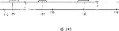
图24A、25A、26A和28A是图22和图23所示的薄膜晶体管阵列板的在按本发明实施例的薄膜晶体管阵列板制造方法的中间步骤中的布图;24A, 25A, 26A and 28A are the layout diagrams of the TFT array panel shown in FIG. 22 and FIG. 23 in the intermediate steps of the manufacturing method of the TFT array panel according to the embodiment of the present invention;
图24B是图24A所示薄膜晶体管阵列板的沿XXIVB-XXIVB′线切开的剖视图;Figure 24B is a cross-sectional view of the thin film transistor array plate shown in Figure 24A cut along the line XXIVB-XXIVB';
图25B是图25A所示薄膜晶体管阵列板的沿XXVB-XXVB′线切开的剖视图,它显示出图24B所示步骤以后的步骤;Figure 25B is a sectional view cut along the line XXVB-XXVB' of the thin film transistor array plate shown in Figure 25A, which shows the steps after the steps shown in Figure 24B;
图26B是图26A所示薄膜晶体管阵列板的沿XXVIB-XXVIB′线切开的剖视图,它显示出图25B所示步骤以后的步骤;Figure 26B is a sectional view cut along the line XXVIB-XXVIB' of the thin film transistor array plate shown in Figure 26A, which shows the steps after the steps shown in Figure 25B;
图27是图26A所示薄膜晶体管阵列板的沿XXVIB-XXVIB′线切开的剖视图,它显示出图26B所示步骤以后的步骤;以及Figure 27 is a sectional view cut along the line XXVIB-XXVIB' of the thin film transistor array plate shown in Figure 26A, which shows the steps after the steps shown in Figure 26B; and
图28B是图28A所示薄膜晶体管阵列板的沿XXVIIIB-XXVIIIB′线切开的剖视图,它显示出图27所示步骤以后的步骤。28B is a cross-sectional view of the thin film transistor array panel shown in FIG. 28A cut along line XXVIIIB-XXVIIIB', showing steps subsequent to the step shown in FIG. 27. FIG.
具体实施方式Detailed ways
以下参见显示本发明优选实施例的附图更详细地描述本发明。但是,本发明也可以用其他诸多不同形式实施,并且本发明不于所述的实施例。The invention will be described in more detail below with reference to the accompanying drawings showing preferred embodiments of the invention. However, the invention can also be embodied in many different forms and the invention is not limited to the described embodiments.
附图中,为了清楚将层厚、膜、基板、区域等都放大了。相同的附图标记始终指示相同的元件。应了解,当如层、膜、区域或衬底等的元件被称作在另一元件“上”时,该元件可以直接在另一元件上,或者还有居间元件。相反,当说元件“直接放在其他元件上”时,没有居间元件(interveningelement)出现。In the drawings, layer thicknesses, films, substrates, regions, etc. are exaggerated for clarity. The same reference numerals refer to the same elements throughout. It will be understood that when an element such as a layer, film, region, or substrate is referred to as being "on" another element, it can be directly on the other element or intervening elements may also be present. In contrast, when an element is said to be "placed directly on" another element, no intervening elements are present.
现在,参见附图描述按本发实施例的包括接触结构的薄膜晶体管阵列板及其制造方法。Now, a thin film transistor array panel including a contact structure and a manufacturing method thereof according to an embodiment of the present invention will be described with reference to the accompanying drawings.
参见图1和图2详细描述按本发明实施例的用于液晶显示器的薄膜晶体管阵列板。A thin film transistor array panel for a liquid crystal display according to an embodiment of the present invention will be described in detail with reference to FIGS. 1 and 2 .
图1是按本发明实施例的用于液晶显示器的示例性薄膜晶体管阵列板的布图,图2是图1所示薄膜晶体管阵列板的沿II-II′线切开的剖视图。1 is a layout of an exemplary thin film transistor array panel for a liquid crystal display according to an embodiment of the present invention, and FIG. 2 is a cross-sectional view of the thin film transistor array panel shown in FIG. 1 along line II-II'.
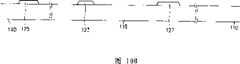
在绝缘衬底110上形成多根栅线121和多根存储电极线131。A plurality of
栅线121和存储电极线131基本按横向方向延伸,并相互隔开。栅线121输送栅极信号,每根栅线121的多个部分形成多个栅极电极123。存储电极线131被供以例如公共电压的预定电压,其被施加给液晶显示器另一基板(未示出)上的公共电极(未示出)。每根存储电极线131包括多个向上和向下突起的扩大部分137。The gate lines 121 and the
栅线121和存储电极线131包括低电阻率导电层,该低电阻率导电层优选用例如Ag和Ag合金的含Ag金属、或者诸如Al和Al合金的含Al金属构成。栅线121和存储电极线131可以具有多层结构,该多层结构包括低电阻率导电层和其他层,其他层优选用对于诸如ITO和IZO的其它材料具有好的物理、化学和电接触特性的Cr、Ti、Ta、Mo或它们的合金如MoW合金制成。这类层的好的示例性组合是Cr和Al-Nd合金。The
栅线121和存储电极线131的侧面是倾斜的。侧面相对于衬底110的表面的倾角范围是约30°-80°。Sides of the
在栅线121和存储电极线131上形成优选用氮化硅(SiNx)构成的栅极绝缘层140。A
在栅极绝缘层140上形成优选用氢化非晶硅(缩写成“a-Si”)构成的多个半导体带151和半导体岛157。每个半导体带151基本上在纵向方向延伸,并具有向着栅极电极123分枝出多个延伸部分154。A plurality of semiconductor strips 151 and
在半导体带151和半导体岛157上形成优选由硅化物或用n型杂质重掺杂的n+氢化a-Si构成的多个欧姆接触带和岛161、165和167。每个欧姆接触带161具有多个延伸部分163,延伸部分163和欧姆接触岛165成对地位于半导体带151的延伸部分154上。欧姆接触岛167位于半导体岛157上。A plurality of ohmic contact strips and
半导体带151和半导体岛157和欧姆接触161、165和167的侧面是倾斜的,其倾角范围优选为约30°-80°。The sides of the
在欧姆接触161、165和167上分别形成多根数据线171、多个漏极电极175和多个存储电容器导体177。A plurality of
数据线171用于输送数据电压,基本上在纵向方向延伸,并与栅线121交叉。每根数据线171的多个分枝向着漏极电极175延伸,形成多个源极电极173。每对源极电极173和漏极电极175相互分开,并关于栅极电极123彼此相对。栅极电极123、源极电极173和漏极电极175以及半导体带151的延伸部分154形成薄膜晶体管,该薄膜晶体管具有在源极电极173和漏极电极175之间设置的延伸部分154中形成的沟道。The data lines 171 are used to transmit data voltages, substantially extend in a longitudinal direction, and cross the gate lines 121 . A plurality of branches of each
存储电容器导体177与存储电极线131的延伸部分137交叠。存储电容器导体177可以延伸到漏极电极175以与其连接。The
数据线171包括物理特性不同的两个膜,下部膜171p和上部膜171q。上部膜171q优选用低电阻率金属构成,例如含Al金属,以减小数据线171中的信号延迟或电压降。另一方面,下部膜171p优选用对于例如ITO和IZO的其他材料具有好的物理、化学和电接触特性的材料制成。用于下部膜171p的示例性材料是Cr、Ti、Ta、Mo及其合金,例如MoW合金,它们还可以用作a-Si和Al之间的扩散阻挡层。数据线171的接触部分,即端部179只包括下部膜而没有上部膜。The
与数据线171类似,漏极电极175和存储电容器导体177也可以具有双层结构,只是接触部分除外。图2显示出双层结构的漏极电极175(175p和175q)、以及单层结构的存储电容器导体177。Similar to the
数据线171、漏极电极175和存储电容器电极177的边缘具有倾斜侧面,其倾角范围是约30°-80°。Edges of the
只在下面的半导体带151和岛157与上面的数据线171、上面的漏极电极175和上面的导体177之间间插有欧姆接触层161、165和167,并减小其间的接触电阻。半导体带151和岛157像数据线171、漏极电极175和存储电容器导体177以及下面的欧姆接触层161、165和167一样具有几乎相同的平面形状,只是提供TFT的延伸部分154除外。具体来说,半导体岛157、欧姆接触岛167和存储导体177具有几乎相同的平面形状。半导体带151包括一些不被数据线171、漏极电极175和存储导体177覆盖的露出部分,例如位于源极电极173和漏极电极175之间的部分。Ohmic contact layers 161, 165 and 167 are interposed only between the
在数据线171、漏极电极175、存储导体177和半导体带151的露出部分上形成钝化层180。钝化层180优选用具有好的平坦特性的光敏有机材料、通过等离子体增强化学气相沉积(PECVD)形成的如a-Si:C:O和a-Si:O:F的低介电绝缘材料、或者例如氮化硅的无机材料形成。A
钝化层180具有多个接触孔185、187和189,用于分别露出漏极电极175、存储导体177和数据线171的端部179。钝化层180和栅极绝缘层140具有多个接触孔182,用于露出栅线121的端部125。The
如上所述,接触孔185和189分别露出漏极电极175的下部膜和数据线171的端部179。此外,接触孔182、185、187和189没有下面切口部分,而小到足以不露出栅线121、漏极电极175、存储电容器导体177和数据线171的边缘。接触孔185和189的边界与上部膜175p和171q的边界不匹配。As described above, the contact holes 185 and 189 expose the lower film of the
在钝化层180上形成优选用IZO或ITO构成的多个像素电极190和多个接触辅助部分(contact assistant)92和97。A plurality of
像素电极190通过接触孔185物理和电连接到漏极电极175,且通过接触孔187物理和电连接到存储电容器导体177,使得像素电极190接收来自漏极电极175的数据电压,和输送收到的数据电压到存储电容器导体177。施加有数据电压的像素电极190与另一基板上的公共电极一起产生电场,该电场使位于其间的液晶分子重取向。The
像素电极190和公共电极形成叫做“液晶电容器”的电容器,该电容器在TFT截止后存储所供给的电压。提供并联连接到液晶电容器上的叫做“存储电容器”的附加电容器,以增强电压存储能力。通过像素电极190和存储电极线131重叠来构成存储电容器。通过在存储电极线131设置扩大部分137以增大重叠面积,并且通过在像素电极190下边设置连接到像素电极190并与扩大部分137重叠的存储电容器导体177以减小接线端(terminal)之间的距离,存储电容器的容量,即存储容量得以增大。The
像素电极190与栅线121和数据线171重叠以增加孔径比(apertureratio),但这是可选的。The
接触辅助部分92和97分别通过接触孔182和189连接到栅线121的露出端部125和数据线171的露出端部179。接触辅助部分92和97不是必须的,但却是优选的,以保护露出部分125和179,并补充露出部分125和179与外部器件的附着力。The contact
如上所述,接触孔185、187和189露出漏极电极175的下部膜,存储电容器电极177和数据线171,同时下部膜具有好的接触特性,且用IZO或ITO构成的像素电极190和接触辅助部分92和97只接触下部膜。因此,降低了它们之间的接触电阻,于是改善了液晶显示器的特性。As mentioned above, the contact holes 185, 187 and 189 expose the lower film of the
按本发明的另一实施例,用透明导电聚合物构成像素电极190。就反射型液晶显示器而言,像素电极190用不透明的反射性金属构成。在这些情况下,可以用与像素电极190不同的材料例如IZO或ITO构成接触辅助部分92和97。According to another embodiment of the present invention, the
现在参见图3A到7B以及图1和图2详细描述按本发明实施例的图1和图2所示的薄膜晶体管阵列板的制造方法。Referring now to FIGS. 3A to 7B and FIGS. 1 and 2, a method of manufacturing the thin film transistor array panel shown in FIGS. 1 and 2 according to an embodiment of the present invention will be described in detail.
图3A、4A、5A和7A是图1和图2所示的薄膜晶体管阵列板的在按本发明实施例的薄膜晶体管阵列板制造方法的中间步骤中的布图;图3B是图3A所示的薄膜晶体管阵列板的沿IIIB-IIIB′线切开的剖视图;图4B是图4A所示薄膜晶体管阵列板的沿IVB-IVB′线切开的剖视图,它显示出图3B所示步骤以后的步骤;图5B是图5A所示薄膜晶体管阵列板的沿VB-VB′线切开的剖视图,它显示出图4B所示步骤以后的步骤;图6是图5A所示薄膜晶体管阵列板的沿VB-VB′线切开的剖视图,它显示出图5B所示步骤以后的步骤;以及图7B是图7A所示的薄膜晶体管阵列板的沿VIIB-VIIB′线切开的剖视图,它显示出图6所示步骤以后的步骤。3A, 4A, 5A and 7A are the layout diagrams of the thin film transistor array plate shown in FIG. 1 and FIG. 2 in the middle steps of the manufacturing method of the thin film transistor array plate according to the embodiment of the present invention; FIG. 3B is the layout shown in FIG. 3A The sectional view of the thin film transistor array plate along IIIB-IIIB' cut; Fig. 4B is the sectional view of the thin film transistor array plate shown in Fig. Step; Fig. 5 B is the cross-sectional view of the thin film transistor array plate shown in Fig. 5A along VB-VB ' line cut, and it shows the step after the step shown in Fig. 4B; Fig. 6 is the edge of the thin film transistor array plate shown in Fig. 5A VB-VB' line cut sectional view, it shows steps after the steps shown in Figure 5B; and Figure 7B is a sectional view cut along VIIB-VIIB' line of the thin film transistor array plate shown in Figure 7A, it shows Steps subsequent to the steps shown in FIG. 6 .
现在参见图3A和3B,在例如透明玻璃的绝缘衬底110上通过光刻蚀刻(photo etching)形成包括多个栅极电极123的多根栅线121和包括多个扩大部分137的多根存储电极线131。Referring now to FIGS. 3A and 3B , on an insulating
用CVD法顺序沉积栅极绝缘层140、本征a-Si层150和非本征a-Si层160。栅极绝缘层140优选用氮化硅构成,其厚度范围是约2000埃到约5000埃,沉积温度范围优选是约250℃到约400℃。The
在非本征a-Si层160上顺序溅镀两层导电膜,下部导电膜和上部导电膜。下部导电膜优选用与IZO和ITO有良好接触特性的Mo、Mo合金或Cr构成,其厚度优选是约500埃。上部导电膜厚度优选是约2500埃,用于上部导电膜的溅射靶包括纯Al或含2atomic%的Nd的Al-Nd,溅射温度是约150℃。Two conductive films, a lower conductive film and an upper conductive film, are sputtered sequentially on the
参见图4A和4B,对上部导电膜和下部导电膜进行光刻蚀刻(photo-etch),以形成包括多个源极电极173的多根数据线171、多个漏极电极175、和多个存储电容器导体177,它们具有包括下部膜171p、175p和177p,以及上部膜171q、175q、和177q的双层结构。对于下部导电膜和上部导电膜可以用任何类型的蚀刻。例如,湿蚀刻和干蚀刻中的任何一种都可以用于下部导电膜和上部导电膜。或者湿蚀刻用于下部导电膜和上部导电膜中的任何一个膜,而干蚀刻用于下部导电膜和上部导电膜中的另一个膜。可以在相同的蚀刻条件下蚀刻含Al金属构成的上部膜和Mo或Mo合金构成的下部膜。Referring to FIGS. 4A and 4B, the upper conductive film and the lower conductive film are photo-etched to form a plurality of
如图5A和5B所示,形成光致抗蚀剂层42。光致抗蚀剂层42不覆盖数据线171、漏极电极175和存储电容器电极177的接触部分,而覆盖非本征a-Si层160的位于源极电极173和漏极电极175之间的部分。用光致抗蚀剂层42作蚀刻掩模蚀刻上部膜171q、175q和177q的露出部分。As shown in FIGS. 5A and 5B, a
用光致抗蚀剂层42以及数据线171、漏极电极175和存储电容器导体177作蚀刻掩模蚀刻非本征a-Si层160和本征a-Si层150,形成多个非本征半导体带和岛164和167,和多个本征半导体带和岛151和157。本征半导体带151包括多个扩大部分154,且其面积大于数据线171和漏极电极175的面积。Use the
除去光致抗蚀剂层42之后,除去非本征半导体带164的露出部分,完成多个欧姆接触带和岛161、165和167,并露出部分本征半导体带151,如图6所示。然后,优选进行氧等离子体处理,以使半导体带151的露出表面稳定。After removing the
总之,只用一个光刻(photolithography)步骤,图5A到图6所示的工艺步骤完成了半导体带和岛151和157,并选择性地除去了数据线171的上部膜等。In summary, with only one photolithography step, the process steps shown in FIGS. 5A to 6 complete the semiconductor strips and
如图7A和7B所示,在沉积钝化层180后,利用光刻来干蚀刻钝化层180和栅极绝缘层140,形成多个接触孔182、185、187和189,分别露出栅线121的端部125、漏极电极175、存储电容器导体177、和数据线171的端部179。As shown in FIGS. 7A and 7B, after the
尽管现有技术要求在形成接触孔182、185、187和189后除去上部膜的露出部分,但是本实施例不需要这样的步骤,因为上部膜没有通过接触孔182、185、187和189露出。因此在接触孔182、185、187和189的接触孔中没有下面切口部分(undercut),因而使侧壁和底部具有光滑的外形。Although the prior art requires removing the exposed portion of the upper film after forming the contact holes 182, 185, 187, and 189, this embodiment does not require such a step because the upper film is not exposed through the contact holes 182, 185, 187, and 189. Therefore, there are no undercuts in the contact holes of the contact holes 182, 185, 187, and 189, thereby giving smooth contours to the sidewalls and bottoms.
最后,如图1和图2所示,在钝化层180上通过溅镀和光刻蚀刻IZO层或ITO层形成多个像素电极190和多个接触辅助部分92和97。用于IZO层的溅射靶的例子是由日本的Idemitsu公司生产的IDIXO(In x-金属氧化物)。溅射靶含In2O3和ZnO,Zn与Zn加In之和的比值范围优选是约15-20atomic%。为了使接触电阻最小的优选溅射温度等于或小于约250℃。Finally, as shown in FIGS. 1 and 2 , a plurality of
如图2所示,像素电极190和接触辅助部分92和97沿着接触孔182、185、187和189的具有光滑外形的侧壁和底部延伸,且具有光滑的外形而没有断开或变形。As shown in FIG. 2, the
在按本发明实施例的薄膜晶体管阵列板中,栅线121和数据线171包括具有低电阻率的Al或Al合金,同时它们与IZO或ITO像素电极190之间的接触电阻减小了。而且,在形成半导体带和岛151和157时不用附加的光刻蚀刻步骤就在接触部分除去了含Al金属层,因而简化了制造工艺。In the thin film transistor array panel according to the embodiment of the present invention, the
参见图8和图9详细说明按本发明另一实施例的用于液晶显示器的薄膜晶体管阵列板。Referring to FIGS. 8 and 9, a thin film transistor array panel for a liquid crystal display according to another embodiment of the present invention will be described in detail.
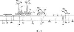
图8是按本发明另一实施例的用于液晶显示器的示例性薄膜晶体管阵列板的布图,图9是图8所示薄膜晶体管阵列板的沿IX-IX′线切开的剖视图。8 is a layout of an exemplary thin film transistor array panel for a liquid crystal display according to another embodiment of the present invention, and FIG. 9 is a cross-sectional view of the thin film transistor array panel shown in FIG. 8 along line IX-IX'.
如图8和图9所示,按本实施例的液晶显示器的薄膜晶体管阵列板的多层结构与图1和图2所示的几乎一样。也就是说,在衬底110上形成有包括多个栅极电极123的多根栅线121,和在其上顺序形成有:栅极绝缘层140、包括多个扩大部分154和多个半导体岛157的多个半导体带151、和包括多个扩大部分163和多个欧姆接触岛165和167的多个欧姆接触带161。在欧姆接触161、165和167上形成有包括多个源极电极173的多根数据线171、多个漏极电极175和多个存储电容器导体177,和在其上形成有钝化层180。在钝化层180和/或栅极绝缘层140上设置有多个接触孔182、185、187和189,且在钝化层180上形成有多个像素电极190和多个接触辅助部分92和97。As shown in FIGS. 8 and 9 , the multilayer structure of the thin film transistor array panel of the liquid crystal display according to this embodiment is almost the same as that shown in FIGS. 1 and 2 . That is, a plurality of
与图1和图2所示的薄膜晶体管阵列板不同,按本实施例的薄膜晶体管阵列板在每根栅线121处设置有多个扩大部分127,并且以存储电容器导体177与栅线121的扩大部分127重叠,形成没有存储电极线的存储电容器。Different from the thin film transistor array board shown in FIG. 1 and FIG. 2, the thin film transistor array board according to this embodiment is provided with a plurality of
半导体带151的宽度大于数据线171的宽度,而图1和图2所示的半导体带151的宽度与数据线171的宽度大致相同。此外,除接触部分179之外,数据线171的几乎所有部分都具有包括下部膜171p和上部膜171q的双层结构,而图1和图2所示的数据线171包括若干个单层部分。具体来说,图8和图9所示的数据线171的下部膜171p和上部膜171q具有大致相同的宽度,而图1和图2所示的每根数据线171的上部膜171q的宽度小于下部膜171p的宽度。The width of the
每个像素电极190的边缘与其附近的半导体带151重叠,而不与其附近的数据线171重叠。当半导体带151的宽度大于数据线171的宽度时,为了获得大的孔径比,栅极电极190与半导体带151的重叠被最小程度地优选。The edge of each
现在参见图10A-14B以及图8和图9详细描述按本发明实施例的图8和图9所示的薄膜晶体管阵列板的制造方法。Referring now to FIGS. 10A-14B and FIGS. 8 and 9 , the manufacturing method of the thin film transistor array panel shown in FIGS. 8 and 9 according to the embodiment of the present invention will be described in detail.
图10A、11A、12A和14A是图8和图9所示薄膜晶体管阵列板的在按本发明实施例的薄膜晶体管阵列板制造方法的中间步骤中的布图;图10B是图10A所示薄膜晶体管阵列板的沿XB-XB′线切开的剖视图;图11B是图11A所示薄膜晶体管阵列板的沿XIB-XIB′线切开的剖视图,它显示出图10B所示步骤以后的步骤;图12B是图12A所示薄膜晶体管阵列板的沿XIIB-XIIB′线切开的剖视图,它显示出图11B所示步骤以后的步骤;图13是图12A所示薄膜晶体管阵列板的沿XIIB-XIIB′线切开的剖视图,它显示出图12B所示步骤以后的步骤;以及图14B是图14A所示的薄膜晶体管阵列板的沿XIVB-XIVB′线切开的剖视图,它显示出图13所示步骤以后的步骤。10A, 11A, 12A and 14A are the layout diagrams of the thin film transistor array plate shown in FIG. 8 and FIG. 9 in the intermediate steps of the manufacturing method of the thin film transistor array plate according to the embodiment of the present invention; The cross-sectional view of the transistor array plate cut along the XB-XB' line; Figure 11B is a cross-sectional view of the thin film transistor array plate shown in Figure 11A along the XIB-XIB' line, which shows the steps after the steps shown in Figure 10B; Fig. 12B is the cross-sectional view of the thin film transistor array board shown in Fig. 12A along XIIB-XIIB ' line, it shows the step after the step shown in Fig. 11B; Fig. 13 is the thin film transistor array board shown in Fig. 12A along XIIB- XIIB' line cut sectional view, it shows the steps after the step shown in Figure 12B; Step after the step shown.
参见图10A和10B,在例如透明玻璃的绝缘衬底110上用光刻蚀刻法形成包括多个栅极电极123和多个扩大部分127的多根栅线121。Referring to FIGS. 10A and 10B, a plurality of
在顺序沉积栅极绝缘层140、本征a-Si层150和非本征a-Si层160后,在其上顺序溅镀下部导电膜和上部导电膜。下部导电膜优选用与IZO和ITO有良好接触特性的Mo、Mo合金或Cr构成,其厚度优选是约500埃。上部导电膜厚度优选是约2500埃,用于上部导电膜的溅射靶包括纯Al或含2atomic%的Nd的Al-Nd,溅射温度是约150℃。After sequentially depositing the
参见图11A和11B,对上部膜和下部膜进行光刻蚀刻,形成包括多个源极电极173的多根数据线171、多个漏极电极175和多个存储电容器导体177,它具有包括下部膜171p、175p和177p,以及上部膜171q、175q和177q的双层结构。11A and 11B, the upper film and the lower film are photolithographically etched to form a plurality of
如图12A和12B所示,形成光致抗蚀剂层44。光致抗蚀剂层44不覆盖数据线171、漏极电极175和存储电容器电极177的接触部分,而覆盖非本征a-Si层160的位于源极电极173和漏极电极175之间的部分。用光致抗蚀剂层44作蚀刻掩模蚀刻上部膜171q、175q和177q的露出部分。As shown in FIGS. 12A and 12B, a
用光致抗蚀剂层44以及数据线171、漏极电极175和存储电容器导体177作蚀刻掩模蚀刻非本征a-Si层160和本征a-Si层150,形成多个非本征半导体带和岛164和167,和多个本征半导体带和岛151和157。除去光致抗蚀剂层44之后,除去非本征半导体带164的露出部分,完成多个欧姆接触带和岛161、165和167,和露出下面的部分本征半导体带151,如图13所示。Use the
如图14A和14B所示,在沉积钝化层180后,利用光刻干蚀刻钝化层180和栅极绝缘层140,形成多个接触孔182、185、187和189,分别露出栅线121的端部125、漏极电极175、存储电容器导体177和数据线171的端部179。As shown in FIGS. 14A and 14B, after depositing the
最后,如图8和图9所示,在钝化层180上形成多个像素电极190和多个接触辅助部分92和97。Finally, as shown in FIGS. 8 and 9 , a plurality of
在按本发明实施例的薄膜晶体管阵列板中,栅线121和数据线171包括具有低电阻率的Al或Al合金,同时它们与IZO或ITO像素电极190之间的接触电阻减小了。而且,在形成半导体带和岛151和157时不用附加的光刻蚀刻步骤就除去了在接触部分处的含Al金属层,因而简化了制造工艺。In the thin film transistor array panel according to the embodiment of the present invention, the
参见图15和图16详细说明按本发明另一实施例的用于液晶显示器的薄膜晶体管阵列板。Referring to FIGS. 15 and 16, a thin film transistor array panel for a liquid crystal display according to another embodiment of the present invention will be described in detail.
图15是按本发明另一实施例的用于液晶显示器的示例性薄膜晶体管阵列板的布图;图16是图15所示薄膜晶体管阵列板的沿XVI-XVI′线切开的剖视图。15 is a layout of an exemplary TFT array panel for a liquid crystal display according to another embodiment of the present invention; FIG. 16 is a cross-sectional view of the TFT array panel shown in FIG. 15 along line XVI-XVI'.
如图15和图16所示,按本实施例的液晶显示器的薄膜晶体管阵列板的结构与图1和图2所示的几乎一样。也就是说,在衬底110上形成有包括多个栅极电极123的多根栅线121和包括多个扩大部分的多根存储电极线131,且在其上顺序形成有:栅极绝缘层140、包括多个扩大部分154和多个半导体岛157的多个半导体带151、和包括多个扩大部分163和多个欧姆接触岛165和167的多个欧姆接触带161。在欧姆接触部161、165和167上形成有包括多个源极电极173的多根数据线171、多个漏极电极175和多个存储电容器导体177,且在其上形成有钝化层180。在钝化层180和/或栅极绝缘层140上设置有多个接触孔182、185、187和189,且在钝化层180上形成有多个像素电极190和多个接触辅助部分92和97。As shown in FIGS. 15 and 16, the structure of the thin film transistor array panel of the liquid crystal display according to this embodiment is almost the same as that shown in FIGS. 1 and 2 . That is, a plurality of
与图1和图2所示的薄膜晶体管阵列板不同,按本实施例的薄膜晶体管阵列板在数据线171、漏极电极175和存储电容器导体177的通过接触孔189、185和187露出的接触部分的表面上形成不平坦。Different from the thin film transistor array board shown in FIG. 1 and FIG. 2, the thin film transistor array board according to this embodiment has contacts exposed through the contact holes 189, 185 and 187 on the
现在,参见图17A-21B以及图15和16详细描述按本发明实施例的图15和16所示的薄膜晶体管阵列板的制造方法。Now, referring to FIGS. 17A-21B and FIGS. 15 and 16, the manufacturing method of the thin film transistor array panel shown in FIGS. 15 and 16 according to the embodiment of the present invention will be described in detail.
图17A、18A、19A和21A是图15和图16所示薄膜晶体管阵列板的在按本发明实施例的薄膜晶体管阵列板制造方法的中间步骤中的布图;图17B是图17A所示薄膜晶体管阵列板的沿XVIIB-XVIIB′线切开的剖视图;图18B是图18A所示薄膜晶体管阵列板的沿XVIIIB-XVIIIB′线切开的剖视图,它显示出图17B所示步骤以后的步骤;图19B是图19A所示薄膜晶体管阵列板的沿XIXB-XIXB′线切开的剖视图,它显示出图18B所示步骤以后的步骤;图20是图19A所示薄膜晶体管阵列板的沿XIXB-XIXB′线切开的剖视图,它显示出图19B所示步骤以后的步骤;以及图21B是图21A所示薄膜晶体管阵列板的沿XXIB-XXIB′线切开的剖视图,它显示出图20所示步骤以后的步骤。17A, 18A, 19A and 21A are the layout diagrams of the TFT array panel shown in FIG. 15 and FIG. 16 in the intermediate steps of the manufacturing method of the TFT array panel according to the embodiment of the present invention; FIG. 17B is the layout of the TFT array panel shown in FIG. The cross-sectional view of the transistor array plate cut along the line XVIIB-XVIIB'; Figure 18B is a cross-sectional view of the thin film transistor array plate shown in Figure 18A along the XVIIIB-XVIIIB' line, which shows the steps after the steps shown in Figure 17B; Figure 19B is a sectional view cut along the line XIXB-XIXB' of the thin film transistor array plate shown in Figure 19A, which shows the steps after the steps shown in Figure 18B; XIXB' line cut sectional view, it shows the steps after the step shown in Figure 19B; Steps after the step shown.
参见图17A和17B,在例如透明玻璃的绝缘衬底110上用光刻蚀刻法形成包括多个栅极电极123的多根栅线121和包括多个扩大部分137的多根存储电极线131。Referring to FIGS. 17A and 17B, a plurality of
在顺序沉积栅极绝缘层140、本征a-Si层150和非本征a-Si层160后,在其上顺序溅镀下部导电膜和上部导电膜。下部导电膜优选用与IZO和ITO有良好接触特性的Mo、Mo合金或Cr构成,其厚度优选是约500埃。上部导电膜厚度优选是约2500埃,用于上部导电膜的溅射靶包括纯Al或含2atomic%的Nd的A1-Nd,溅射温度是约150℃。After sequentially depositing the
参见图18A和18B,对上部导电膜和下部导电膜进行光刻蚀刻,形成包括多个源极电极173的多根数据线171、多个漏极电极175和多个存储电容器导体177,它具有包括下部膜171p、175p和177p,和上部膜171q、175q和177q的双层结构。18A and 18B, the upper conductive film and the lower conductive film are photolithographically etched to form a plurality of
如图19A和19B所示,形成光致抗蚀剂层46。光致抗蚀剂层46覆盖数据线171、漏极电极175和存储电容器电极177的接触部分的一部分,而不覆盖接触部分的其余部分,而且覆盖非本征a-Si层160的位于源极电极173和漏极电极175之间的部分。光致抗蚀剂层46的在接触部分上的部分与其他部分隔开,并可以具有各种形状,尽管图19A所示部分的形状是矩形。用光致抗蚀剂层46作蚀刻掩模蚀刻上部膜171q、175q和177q的露出部分。然后,多个导电岛175q、177q和179q留在漏极电极175、存储电容器导体177和数据线171的接触部分上。As shown in FIGS. 19A and 19B, a
用光致抗蚀剂层46以及数据线171、漏极电极175和存储电容器导体177作蚀刻掩模来干蚀刻非本征a-Si层160和本征a-Si层150,形成多个非本征半导体带和岛164和167、以及多个本征半导体带和岛151和157。在除去光致抗蚀剂层46之后,通过干蚀刻除去非本征半导体带164的露出部分,完成多个欧姆接触带和岛161、165和167,并露出下面的部分本征半导体带151,如图20所示。Use the
如上所述,执行多个干蚀刻步骤以构图非本征a-Si层160、本征a-Si层150和非本征半导体带164。光致抗蚀剂层46和在漏极电极175、存储电容器导体177和数据线171上的导电岛175q、177q和179q保护下部膜175p、177p和179p的在其下的部分不被干蚀刻。相反,可以对下部膜175p、177p和179p的露出部分进行一定程度的蚀刻。As described above, multiple dry etch steps are performed to pattern the
如图21A和21B所示,在沉积钝化层180后,利用光刻干蚀刻钝化层180和栅极绝缘层140,形成多个接触孔182、185、187和189,分别露出栅线121的端部125、漏极电极175、存储电容器导体177和数据线171的端部179。钝化层180的干蚀刻还在接触孔185、187和189处雕刻出下部膜175p、177p和179p的露出部分,而不会蚀刻下部膜175p、177p和179p的被导电岛175q、177q和179q覆盖的受保护部分。因此下部膜175p、177p和179p的表面不平坦。As shown in FIGS. 21A and 21B, after the
随后,经表面蚀刻除去导电岛175q、177q和179q,露出下面的下部膜175p、177p和179p的清洁表面。Subsequently, the
最后,如图15和图16所示,在钝化层180上形成多个像素电极190和多个接触辅助部分92和97。Finally, as shown in FIGS. 15 and 16 , a plurality of
由于像素电极190和接触辅助部分92和97接触不平坦的下部膜175p、177p和179p的清洁表面,所以减小了它们之间的接触电阻。Since the
现在参见图22和图23详细描述按本发明另一实施例的用于液晶显示器的薄膜晶体管阵列板。Referring now to FIGS. 22 and 23, a thin film transistor array panel for a liquid crystal display according to another embodiment of the present invention will be described in detail.
图22是按本发明另一实施例的用于液晶显示器的示例性薄膜晶体管阵列板的布图;图23是图22所示薄膜晶体管阵列板的沿XXIII-XXIII′线切开的剖视图。22 is a layout of an exemplary TFT array panel for a liquid crystal display according to another embodiment of the present invention; FIG. 23 is a cross-sectional view of the TFT array panel shown in FIG. 22 along line XXIII-XXIII'.
如图22和图23所示,按本实施例的液晶显示器的薄膜晶体管阵列板的结构与图8和图9所示的几乎一样。也就是说,在衬底110上形成有包括多个栅极电极123和多个扩大部分127的多根栅线121,和在其上顺序形成有:栅极绝缘层140、包括多个扩大部分154和多个半导体岛157的多个半导体带151、和包括多个扩大部分163和多个欧姆接触岛165和167的多个欧姆接触带161。在欧姆接触部161、165和167上形成有包括多个源极电极173的多根数据线171、多个漏极电极175和多个存储电容器导体177,和在其上形成有钝化层180。在钝化层180和/或栅极绝缘层140上设置有多个接触孔182、185、187和189,且在钝化层180上形成有多个像素电极190和多个接触辅助部分92和97。As shown in FIGS. 22 and 23, the structure of the thin film transistor array panel of the liquid crystal display according to this embodiment is almost the same as that shown in FIGS. 8 and 9 . That is, a plurality of
与图8和图9所示的薄膜晶体管阵列板不同,与图15和图16所示的类似,按本实施例的薄膜晶体管阵列板在数据线171、漏极电极175和存储电容器导体177的通过接触孔189、185和187露出的接触部分的表面上提供有不平坦。Different from the thin film transistor array board shown in FIG. 8 and FIG. 9, similar to that shown in FIG. 15 and FIG. Unevenness is provided on the surface of the contact portion exposed through the contact holes 189 , 185 and 187 .
现在,参见图24-28B以及图22和23详细说明按本发明实施例的图22和23所示的晶体管阵列板的制造方法。Now, referring to FIGS. 24-28B and FIGS. 22 and 23, the manufacturing method of the transistor array panel shown in FIGS. 22 and 23 according to the embodiment of the present invention will be described in detail.
图23是图22所示薄膜晶体管阵列板的沿XXIII-XXIII′线切开的剖视图;图24A、25A、26A和28A是图22和图23所示的薄膜晶体管阵列板的在按本发明实施例的薄膜晶体管阵列板制造方法的中间步骤中的布图;图24B是图24A所示薄膜晶体管阵列板的沿XXIVB-XXIVB′线切开的剖视图;图25B是图25A所示薄膜晶体管阵列板的沿XXVB-XXVB′线切开的剖视图,它显示出图24B所示步骤以后的步骤;图26B是图26A所示薄膜晶体管阵列板的沿XXVIB-XXVIB′线切开的剖视图,它显示出图25B所示步骤以后的步骤;图27是图26A所示薄膜晶体管阵列板的沿XXVIB-XXVIB′线切开的剖视图,它显示出图26B所示步骤以后的步骤;以及图28B是图28A所示薄膜晶体管阵列板的沿XXVIIIB-XXVIIIB′线切开的剖视图,它显示出图27所示步骤以后的步骤。Fig. 23 is the cross-sectional view of the thin film transistor array plate shown in Fig. 22 along XXIII-XXIII' line; Fig. 24A, 25A, 26A and 28A are the thin film transistor array plate shown in Fig. 22 and Fig. 23 in accordance with the implementation of the present invention Figure 24B is a cross-sectional view of the thin film transistor array plate shown in Figure 24A cut along the line XXIVB-XXIVB'; Figure 25B is a thin film transistor array plate shown in Figure 25A The sectional view cut along the XXVB-XXVB' line, it shows the steps after the steps shown in Figure 24B; Figure 26B is a sectional view cut along the XXVIB-XXVIB' line of the thin film transistor array plate shown in Figure 26A, it shows Steps after the steps shown in Figure 25B; Figure 27 is a sectional view cut along the line XXVIB-XXVIB' of the thin film transistor array plate shown in Figure 26A, which shows the steps after the steps shown in Figure 26B; and Figure 28B is a step after the steps shown in Figure 28A A cross-sectional view of the thin film transistor array panel taken along the line XXVIIIB-XXVIIIB' is shown, which shows steps after the step shown in FIG. 27 .
参见图24A和24B,在例如透明玻璃的绝缘衬底110上用光刻蚀刻法形成包括多个栅极电极123和多个扩大部分127的多根栅线121。Referring to FIGS. 24A and 24B, a plurality of
在顺序沉积栅极绝缘层140、本征a-Si层150和非本征a-Si层160后,在其上顺序溅镀下部导电膜和上部导电膜。下部导电膜优选用与IZO和ITO有良好接触特性的Mo、Mo合金或Cr构成,其厚度优选是约500埃。上部导电膜厚度优选是约2500埃,用于上部导电膜的溅射靶包括纯Al或含2atomic%的Nd的Al-Nd,溅射温度是约150℃。After sequentially depositing the
参见图25A和25B,对上部膜和下部膜进行光刻蚀刻,形成包括多个源极电极173的多根数据线171、多个漏极电极175和多个存储电容器导体177,它们具有包括下部膜171p、175p和177p,和上部膜171q、175q和177q的双层结构。25A and 25B, the upper film and the lower film are photolithographically etched to form a plurality of
在形成光致抗蚀剂层48后,如图26A和26B所示,用光致抗蚀剂层48作蚀刻掩模蚀刻出上部膜171q、175q和177q的露出部分。然后在漏极电极175、存储电容器导体177和数据线171的接触部分上留下多个导电岛175q、177q和179q。After forming the
用光致抗蚀剂层48以及数据线171、漏极电极175和存储电容器电极177作蚀刻掩模干蚀刻非本征a-Si层160和本征a-Si层150,以形成多个非本征半导体带和岛164和167,和多个本征半导体带和岛151和157。除去光致抗蚀剂层48之后,通过干蚀刻除去非本征半导体带164的露出部分,完成多个欧姆接触带和岛161、165和167,和露出本征半导体带151的在其下的部分,如图27所示。Use the
光致抗蚀剂岛48和在漏极电极175、存储电容器导体177和数据线171上的导电岛175q、177q和179q保护了下部膜175p、177p和179p的在其下的部分不被干蚀刻。相反,可以对下部膜175p、177p和179p的露出部分进行一定程度的蚀刻。
如图28A和28B所示,在沉积钝化层180后,利用光刻干蚀刻钝化层180和栅极绝缘层140,形成多个接触孔182、185、187和189,分别露出栅线121的端部125、漏极电极175、存储电容器导体177和数据线171的端部179。钝化层180的干蚀刻还在接触孔185、187和189处雕刻出下部膜175p、177p和179p的露出部分,而不会蚀刻下部膜175p、177p和179p的被导电岛175q、177q和179q覆盖的受保护部分。因此下部膜175p、177p和179p的表面不平坦。As shown in FIGS. 28A and 28B, after the
随后,通过表面蚀刻除去导电岛175q、177q和179q,露出其下的下部膜175p、177p和179p的清洁表面。Subsequently, the
最后,如图22和图23所示,在钝化层180上形成多个像素电极190和多个接触辅助部分92和97。Finally, as shown in FIGS. 22 and 23 , a plurality of
由于像素电极190和接触辅助部分92和97接触具有不平坦的下部膜175p、177p和179p的清洁表面,所以减小了它们之间的接触电阻。Since the
尽管以上参见优选实施例详细描述了本发明,但是,本领域技术人员应了解,在不脱离所附的权利要求书界定的本发明的精神和范围的前提下还会有各种改进和替换。Although the present invention has been described in detail above with reference to the preferred embodiments, those skilled in the art should understand that various improvements and substitutions can be made without departing from the spirit and scope of the present invention defined by the appended claims.
Claims (19)
Applications Claiming Priority (6)
| Application Number | Priority Date | Filing Date | Title |
|---|---|---|---|
| KR1020020042659AKR100878238B1 (en) | 2002-07-19 | 2002-07-19 | Thin film transistor array substrate and manufacturing method thereof |
| KR0042659/2002 | 2002-07-19 | ||
| KR0042659/02 | 2002-07-19 | ||
| KR0068107/2002 | 2002-11-05 | ||
| KR0068107/02 | 2002-11-05 | ||
| KR1020020068107AKR100878278B1 (en) | 2002-11-05 | 2002-11-05 | Thin film transistor array substrate and manufacturing method thereof |
Related Child Applications (1)
| Application Number | Title | Priority Date | Filing Date |
|---|---|---|---|
| CNA2006101727220ADivisionCN1992295A (en) | 2002-07-19 | 2003-07-19 | Thin film transistor array panel and manufacturing method thereof |
Publications (2)
| Publication Number | Publication Date |
|---|---|
| CN1495851A CN1495851A (en) | 2004-05-12 |
| CN100378902Ctrue CN100378902C (en) | 2008-04-02 |
Family
ID=31949615
Family Applications (1)
| Application Number | Title | Priority Date | Filing Date |
|---|---|---|---|
| CNB031514987AExpired - Fee RelatedCN100378902C (en) | 2002-07-19 | 2003-07-19 | Thin film transistor array panel and method of manufacturing the same |
Country Status (4)
| Country | Link |
|---|---|
| US (3) | US7205570B2 (en) |
| JP (1) | JP4644417B2 (en) |
| CN (1) | CN100378902C (en) |
| TW (1) | TWI311815B (en) |
Families Citing this family (41)
| Publication number | Priority date | Publication date | Assignee | Title |
|---|---|---|---|---|
| US6524876B1 (en)* | 1999-04-08 | 2003-02-25 | Samsung Electronics Co., Ltd. | Thin film transistor array panels for a liquid crystal display and a method for manufacturing the same |
| US7205570B2 (en)* | 2002-07-19 | 2007-04-17 | Samsung Electronics Co., Ltd. | Thin film transistor array panel |
| US7172913B2 (en)* | 2004-03-19 | 2007-02-06 | Samsung Electronics Co., Ltd. | Thin film transistor array panel and manufacturing method thereof |
| KR101112538B1 (en)* | 2004-07-27 | 2012-03-13 | 삼성전자주식회사 | THIN film transistor array panel and manufacturing Method thereof |
| JP4802462B2 (en)* | 2004-07-27 | 2011-10-26 | 三菱電機株式会社 | Method for manufacturing thin film transistor array substrate |
| KR20060016920A (en)* | 2004-08-19 | 2006-02-23 | 삼성전자주식회사 | Thin film transistor array panel and manufacturing method thereof |
| KR101066303B1 (en)* | 2004-09-09 | 2011-09-20 | 엘지디스플레이 주식회사 | Thin film transistor array substrate and manufacturing method thereof |
| CN101044627B (en)* | 2004-09-15 | 2012-02-08 | 株式会社半导体能源研究所 | Semiconductor device |
| KR101090252B1 (en)* | 2004-09-24 | 2011-12-06 | 삼성전자주식회사 | Thin film transistor array panel and manufacturing method thereof |
| KR20060030577A (en) | 2004-10-06 | 2006-04-11 | 삼성전자주식회사 | Thin film transistor array panel |
| TWI252587B (en) | 2004-12-14 | 2006-04-01 | Quanta Display Inc | Method for manufacturing a pixel electrode contact of a thin-film transistors liquid crystal display |
| CN100371814C (en)* | 2005-01-26 | 2008-02-27 | 广辉电子股份有限公司 | Method for manufacturing pixel electrode contact of thin film transistor liquid crystal display |
| KR101160829B1 (en)* | 2005-02-15 | 2012-06-29 | 삼성전자주식회사 | Etchant composition and method for thin film transistor array panel |
| KR101133766B1 (en)* | 2005-03-29 | 2012-04-09 | 삼성전자주식회사 | Method for manufacturing thin film transistor array panel |
| US7911568B2 (en)* | 2005-05-13 | 2011-03-22 | Samsung Electronics Co., Ltd. | Multi-layered thin films, thin film transistor array panel including the same, and method of manufacturing the panel |
| KR101369864B1 (en)* | 2005-08-12 | 2014-03-05 | 가부시키가이샤 한도오따이 에네루기 켄큐쇼 | Semiconductor device and method for manufacturing the same |
| KR101184640B1 (en)* | 2006-03-15 | 2012-09-20 | 삼성디스플레이 주식회사 | Thin film transistor panel and method of manufacturing for the same |
| CN100426511C (en)* | 2006-06-23 | 2008-10-15 | 北京京东方光电科技有限公司 | Baseplate structure of thin film transistor device array, and preparation method |
| CN100433338C (en)* | 2006-06-23 | 2008-11-12 | 北京京东方光电科技有限公司 | Baseplate structure of thin film transistor device array, and preparation method |
| KR20080000788A (en)* | 2006-06-28 | 2008-01-03 | 삼성전자주식회사 | Thin film transistor array panel and manufacturing method thereof |
| US8283724B2 (en)* | 2007-02-26 | 2012-10-09 | Semiconductor Energy Laboratory Co., Ltd. | Memory element and semiconductor device, and method for manufacturing the same |
| US9064845B2 (en) | 2007-06-25 | 2015-06-23 | Sensor Electronic Technology, Inc. | Methods of fabricating a chromium/titanium/aluminum-based semiconductor device contact |
| US9514947B2 (en) | 2007-06-25 | 2016-12-06 | Sensor Electronic Technology, Inc. | Chromium/titanium/aluminum-based semiconductor device contact fabrication |
| US8766448B2 (en)* | 2007-06-25 | 2014-07-01 | Sensor Electronic Technology, Inc. | Chromium/Titanium/Aluminum-based semiconductor device contact |
| US7738050B2 (en)* | 2007-07-06 | 2010-06-15 | Semiconductor Energy Laboratory Co., Ltd | Liquid crystal display device |
| KR101414043B1 (en)* | 2007-12-04 | 2014-07-21 | 삼성디스플레이 주식회사 | Thin film transistor substrate |
| TW201039034A (en)* | 2009-04-27 | 2010-11-01 | Chunghwa Picture Tubes Ltd | Pixel structure and the method of forming the same |
| KR101571803B1 (en)* | 2009-06-09 | 2015-11-26 | 삼성디스플레이 주식회사 | Array substrate and method of manufacturing the array substrate |
| TWI700810B (en) | 2009-08-07 | 2020-08-01 | 日商半導體能源研究所股份有限公司 | Semiconductor device and method for manufacturing the same |
| TWI426566B (en)* | 2009-11-05 | 2014-02-11 | Univ Nat Taiwan | Thin-film transistor and forming method thereof |
| KR101582946B1 (en)* | 2009-12-04 | 2016-01-08 | 삼성디스플레이 주식회사 | Thin film transistor display panel and manufacturing method thereof |
| WO2011070901A1 (en)* | 2009-12-11 | 2011-06-16 | Semiconductor Energy Laboratory Co., Ltd. | Semiconductor device and manufacturing method thereof |
| US8288767B2 (en)* | 2010-01-04 | 2012-10-16 | National Taiwan University | Thin-film transistor and forming method thereof |
| KR20110116803A (en)* | 2010-04-20 | 2011-10-26 | 삼성전자주식회사 | Display substrate, liquid crystal display comprising same and method for manufacturing same |
| KR101741732B1 (en) | 2010-05-07 | 2017-05-31 | 삼성디스플레이 주식회사 | Thin film transistor panel and method of manufacturing the same |
| JP5667868B2 (en)* | 2010-12-24 | 2015-02-12 | 株式会社半導体エネルギー研究所 | Method for manufacturing semiconductor device |
| CN104620389B (en) | 2012-09-12 | 2017-11-17 | 夏普株式会社 | Semiconductor device and its manufacture method |
| CN102881598B (en)* | 2012-09-17 | 2015-08-12 | 京东方科技集团股份有限公司 | The manufacture method of thin-film transistor, the manufacture method of array base palte and display unit |
| CN105914227A (en)* | 2016-06-01 | 2016-08-31 | 京东方科技集团股份有限公司 | Wiring structure, array substrate and preparation method thereof, and display panel |
| CN106935598B (en)* | 2017-04-05 | 2019-08-27 | 上海中航光电子有限公司 | Array substrate and manufacturing method thereof, touch panel and touch device |
| KR20220010622A (en)* | 2020-07-16 | 2022-01-26 | 삼성디스플레이 주식회사 | Display device |
Citations (4)
| Publication number | Priority date | Publication date | Assignee | Title |
|---|---|---|---|---|
| CN1165568A (en)* | 1995-10-03 | 1997-11-19 | 精工爱普生株式会社 | Active Matrix Substrate |
| US5986738A (en)* | 1995-10-31 | 1999-11-16 | Sharp Kabushiki Kaisha | Transmission type liquid crystal display device and the method for fabricating the same |
| JPH11352515A (en)* | 1998-06-09 | 1999-12-24 | Mitsubishi Electric Corp | Liquid crystal display device and manufacturing method thereof |
| US6087678A (en)* | 1996-02-29 | 2000-07-11 | Samsung Electronics Co., Ltd. | Thin-film transistor display devices having composite electrodes |
Family Cites Families (14)
| Publication number | Priority date | Publication date | Assignee | Title |
|---|---|---|---|---|
| JPH05323373A (en)* | 1992-05-22 | 1993-12-07 | Fujitsu Ltd | Production of thin film transistor panel |
| JP3281167B2 (en)* | 1994-03-17 | 2002-05-13 | 富士通株式会社 | Method for manufacturing thin film transistor |
| JP4363684B2 (en)* | 1998-09-02 | 2009-11-11 | エルジー ディスプレイ カンパニー リミテッド | Thin film transistor substrate and liquid crystal display device using the same |
| KR100330097B1 (en) | 1998-12-21 | 2002-10-25 | 삼성전자 주식회사 | Thin film transistor substrate for liquid crystal display and manufacturing method thereof |
| KR100623974B1 (en) | 1998-12-08 | 2006-12-05 | 삼성전자주식회사 | Liquid Crystal Display and Manufacturing Method Thereof |
| US6885064B2 (en)* | 2000-01-07 | 2005-04-26 | Samsung Electronics Co., Ltd. | Contact structure of wiring and a method for manufacturing the same |
| TWI253538B (en)* | 2000-09-30 | 2006-04-21 | Au Optronics Corp | Thin film transistor flat display and its manufacturing method |
| KR100720095B1 (en)* | 2000-11-07 | 2007-05-18 | 삼성전자주식회사 | Thin film transistor array substrate and manufacturing method thereof |
| KR100729764B1 (en) | 2000-11-15 | 2007-06-20 | 삼성전자주식회사 | Manufacturing method of thin film transistor substrate for liquid crystal display device |
| US6511869B2 (en)* | 2000-12-05 | 2003-01-28 | International Business Machines Corporation | Thin film transistors with self-aligned transparent pixel electrode |
| JP2002296609A (en)* | 2001-03-29 | 2002-10-09 | Nec Corp | Liquid crystal display device and its manufacturing method |
| KR20020083249A (en) | 2001-04-26 | 2002-11-02 | 삼성전자 주식회사 | A contact structure of a wires and method manufacturing the same, and thin film transistor substrate including the contact structure and method manufacturing the same |
| KR100864490B1 (en) | 2002-06-07 | 2008-10-20 | 삼성전자주식회사 | The contact portion of the wiring and the thin film transistor substrate including the same |
| US7205570B2 (en)* | 2002-07-19 | 2007-04-17 | Samsung Electronics Co., Ltd. | Thin film transistor array panel |
- 2003
- 2003-07-15USUS10/619,668patent/US7205570B2/ennot_activeExpired - Fee Related
- 2003-07-16TWTW092119459Apatent/TWI311815B/ennot_activeIP Right Cessation
- 2003-07-18JPJP2003277161Apatent/JP4644417B2/ennot_activeExpired - Fee Related
- 2003-07-19CNCNB031514987Apatent/CN100378902C/ennot_activeExpired - Fee Related
- 2007
- 2007-03-01USUS11/680,739patent/US7632723B2/ennot_activeExpired - Fee Related
- 2007-03-01USUS11/680,733patent/US7615784B2/ennot_activeExpired - Fee Related
Patent Citations (4)
| Publication number | Priority date | Publication date | Assignee | Title |
|---|---|---|---|---|
| CN1165568A (en)* | 1995-10-03 | 1997-11-19 | 精工爱普生株式会社 | Active Matrix Substrate |
| US5986738A (en)* | 1995-10-31 | 1999-11-16 | Sharp Kabushiki Kaisha | Transmission type liquid crystal display device and the method for fabricating the same |
| US6087678A (en)* | 1996-02-29 | 2000-07-11 | Samsung Electronics Co., Ltd. | Thin-film transistor display devices having composite electrodes |
| JPH11352515A (en)* | 1998-06-09 | 1999-12-24 | Mitsubishi Electric Corp | Liquid crystal display device and manufacturing method thereof |
Also Published As
| Publication number | Publication date |
|---|---|
| US7205570B2 (en) | 2007-04-17 |
| TW200402888A (en) | 2004-02-16 |
| US7615784B2 (en) | 2009-11-10 |
| TWI311815B (en) | 2009-07-01 |
| US20040056251A1 (en) | 2004-03-25 |
| CN1495851A (en) | 2004-05-12 |
| US7632723B2 (en) | 2009-12-15 |
| US20070138481A1 (en) | 2007-06-21 |
| US20070138474A1 (en) | 2007-06-21 |
| JP4644417B2 (en) | 2011-03-02 |
| JP2004056153A (en) | 2004-02-19 |
Similar Documents
| Publication | Publication Date | Title |
|---|---|---|
| CN100378902C (en) | Thin film transistor array panel and method of manufacturing the same | |
| US6642580B1 (en) | Thin film transistor array substrate and manufacturing method thereof | |
| US8218117B2 (en) | Liquid crystal display and method of manufacturing the same | |
| JP4481759B2 (en) | Thin film transistor array panel and manufacturing method thereof | |
| CN1519955B (en) | Thin film transistor array panel, method of manufacturing the same, and mask for the same | |
| US7666697B2 (en) | Thin film transistor substrate and method of manufacturing the same | |
| US20080299712A1 (en) | Manufacturing method of a thin film transistor array panel | |
| US20090002587A1 (en) | Thin film transistor array panel and a manufacturing method thereof | |
| JP2014093521A (en) | Thin film transistor array substrate and method for manufacturing the same | |
| KR101046928B1 (en) | Thin film transistor array panel and manufacturing method | |
| KR20060028519A (en) | Thin film transistor array panel and manufacturing method | |
| KR101160823B1 (en) | Thin film transistor array panel and manufacturing method thereof | |
| JP2004013003A (en) | Liquid crystal display | |
| KR100973809B1 (en) | Thin film transistor array panel and manufacturing method thereof | |
| US20170263646A1 (en) | Thin film transistor array panel and a method for manufacturing the same | |
| JP2003215634A (en) | Thin film transistor liquid crystal display device | |
| KR20060020895A (en) | Method of manufacturing thin film transistor array panel | |
| KR20060023396A (en) | Thin film transistor array panel and manufacturing method thereof | |
| KR20050114399A (en) | Thin film transistor array panel and manufacturing method thereof | |
| KR20060082313A (en) | Liquid crystal display | |
| KR20070070738A (en) | Method of manufacturing thin film transistor array panel | |
| KR20060063250A (en) | Method of manufacturing thin film transistor array panel | |
| KR20050106196A (en) | Thin film transistor array panel and manufacturing method thereof |
Legal Events
| Date | Code | Title | Description |
|---|---|---|---|
| C06 | Publication | ||
| PB01 | Publication | ||
| C10 | Entry into substantive examination | ||
| SE01 | Entry into force of request for substantive examination | ||
| C14 | Grant of patent or utility model | ||
| GR01 | Patent grant | ||
| ASS | Succession or assignment of patent right | Owner name:SAMSUNG MONITOR CO., LTD. Free format text:FORMER OWNER: SAMSUNG ELECTRONICS CO., LTD. Effective date:20121029 | |
| C41 | Transfer of patent application or patent right or utility model | ||
| TR01 | Transfer of patent right | Effective date of registration:20121029 Address after:Gyeonggi Do, South Korea Patentee after:Samsung Display Co., Ltd. Address before:Gyeonggi Do, South Korea Patentee before:Samsung Electronics Co., Ltd. | |
| C17 | Cessation of patent right | ||
| CF01 | Termination of patent right due to non-payment of annual fee | Granted publication date:20080402 Termination date:20120719 |