CN100378779C - Electroluminescence display device and driving method thereof - Google Patents
Electroluminescence display device and driving method thereofDownload PDFInfo
- Publication number
- CN100378779C CN100378779CCNB2004100426424ACN200410042642ACN100378779CCN 100378779 CCN100378779 CCN 100378779CCN B2004100426424 ACNB2004100426424 ACN B2004100426424ACN 200410042642 ACN200410042642 ACN 200410042642ACN 100378779 CCN100378779 CCN 100378779C
- Authority
- CN
- China
- Prior art keywords
- line
- gate
- bar
- display device
- gate line
- Prior art date
- Legal status (The legal status is an assumption and is not a legal conclusion. Google has not performed a legal analysis and makes no representation as to the accuracy of the status listed.)
- Expired - Lifetime
Links
Images


Classifications
- G—PHYSICS
- G09—EDUCATION; CRYPTOGRAPHY; DISPLAY; ADVERTISING; SEALS
- G09G—ARRANGEMENTS OR CIRCUITS FOR CONTROL OF INDICATING DEVICES USING STATIC MEANS TO PRESENT VARIABLE INFORMATION
- G09G3/00—Control arrangements or circuits, of interest only in connection with visual indicators other than cathode-ray tubes
- G09G3/20—Control arrangements or circuits, of interest only in connection with visual indicators other than cathode-ray tubes for presentation of an assembly of a number of characters, e.g. a page, by composing the assembly by combination of individual elements arranged in a matrix no fixed position being assigned to or needed to be assigned to the individual characters or partial characters
- G09G3/22—Control arrangements or circuits, of interest only in connection with visual indicators other than cathode-ray tubes for presentation of an assembly of a number of characters, e.g. a page, by composing the assembly by combination of individual elements arranged in a matrix no fixed position being assigned to or needed to be assigned to the individual characters or partial characters using controlled light sources
- G09G3/30—Control arrangements or circuits, of interest only in connection with visual indicators other than cathode-ray tubes for presentation of an assembly of a number of characters, e.g. a page, by composing the assembly by combination of individual elements arranged in a matrix no fixed position being assigned to or needed to be assigned to the individual characters or partial characters using controlled light sources using electroluminescent panels
- G09G3/32—Control arrangements or circuits, of interest only in connection with visual indicators other than cathode-ray tubes for presentation of an assembly of a number of characters, e.g. a page, by composing the assembly by combination of individual elements arranged in a matrix no fixed position being assigned to or needed to be assigned to the individual characters or partial characters using controlled light sources using electroluminescent panels semiconductive, e.g. using light-emitting diodes [LED]
- G09G3/3208—Control arrangements or circuits, of interest only in connection with visual indicators other than cathode-ray tubes for presentation of an assembly of a number of characters, e.g. a page, by composing the assembly by combination of individual elements arranged in a matrix no fixed position being assigned to or needed to be assigned to the individual characters or partial characters using controlled light sources using electroluminescent panels semiconductive, e.g. using light-emitting diodes [LED] organic, e.g. using organic light-emitting diodes [OLED]
- G09G3/3225—Control arrangements or circuits, of interest only in connection with visual indicators other than cathode-ray tubes for presentation of an assembly of a number of characters, e.g. a page, by composing the assembly by combination of individual elements arranged in a matrix no fixed position being assigned to or needed to be assigned to the individual characters or partial characters using controlled light sources using electroluminescent panels semiconductive, e.g. using light-emitting diodes [LED] organic, e.g. using organic light-emitting diodes [OLED] using an active matrix
- G09G3/3233—Control arrangements or circuits, of interest only in connection with visual indicators other than cathode-ray tubes for presentation of an assembly of a number of characters, e.g. a page, by composing the assembly by combination of individual elements arranged in a matrix no fixed position being assigned to or needed to be assigned to the individual characters or partial characters using controlled light sources using electroluminescent panels semiconductive, e.g. using light-emitting diodes [LED] organic, e.g. using organic light-emitting diodes [OLED] using an active matrix with pixel circuitry controlling the current through the light-emitting element
- G09G3/3241—Control arrangements or circuits, of interest only in connection with visual indicators other than cathode-ray tubes for presentation of an assembly of a number of characters, e.g. a page, by composing the assembly by combination of individual elements arranged in a matrix no fixed position being assigned to or needed to be assigned to the individual characters or partial characters using controlled light sources using electroluminescent panels semiconductive, e.g. using light-emitting diodes [LED] organic, e.g. using organic light-emitting diodes [OLED] using an active matrix with pixel circuitry controlling the current through the light-emitting element the current through the light-emitting element being set using a data current provided by the data driver, e.g. by using a two-transistor current mirror
- G—PHYSICS
- G09—EDUCATION; CRYPTOGRAPHY; DISPLAY; ADVERTISING; SEALS
- G09G—ARRANGEMENTS OR CIRCUITS FOR CONTROL OF INDICATING DEVICES USING STATIC MEANS TO PRESENT VARIABLE INFORMATION
- G09G2300/00—Aspects of the constitution of display devices
- G09G2300/04—Structural and physical details of display devices
- G09G2300/0439—Pixel structures
- G09G2300/0465—Improved aperture ratio, e.g. by size reduction of the pixel circuit, e.g. for improving the pixel density or the maximum displayable luminance or brightness
- G—PHYSICS
- G09—EDUCATION; CRYPTOGRAPHY; DISPLAY; ADVERTISING; SEALS
- G09G—ARRANGEMENTS OR CIRCUITS FOR CONTROL OF INDICATING DEVICES USING STATIC MEANS TO PRESENT VARIABLE INFORMATION
- G09G2300/00—Aspects of the constitution of display devices
- G09G2300/08—Active matrix structure, i.e. with use of active elements, inclusive of non-linear two terminal elements, in the pixels together with light emitting or modulating elements
- G09G2300/0809—Several active elements per pixel in active matrix panels
- G09G2300/0842—Several active elements per pixel in active matrix panels forming a memory circuit, e.g. a dynamic memory with one capacitor
- G—PHYSICS
- G09—EDUCATION; CRYPTOGRAPHY; DISPLAY; ADVERTISING; SEALS
- G09G—ARRANGEMENTS OR CIRCUITS FOR CONTROL OF INDICATING DEVICES USING STATIC MEANS TO PRESENT VARIABLE INFORMATION
- G09G2310/00—Command of the display device
- G09G2310/02—Addressing, scanning or driving the display screen or processing steps related thereto
- G09G2310/0202—Addressing of scan or signal lines
- G09G2310/0205—Simultaneous scanning of several lines in flat panels
Landscapes
- Engineering & Computer Science (AREA)
- Physics & Mathematics (AREA)
- Computer Hardware Design (AREA)
- General Physics & Mathematics (AREA)
- Theoretical Computer Science (AREA)
- Control Of Indicators Other Than Cathode Ray Tubes (AREA)
- Electroluminescent Light Sources (AREA)
- Control Of El Displays (AREA)
- Devices For Indicating Variable Information By Combining Individual Elements (AREA)
Abstract
Translated fromChineseDescription
Translated fromChinese本申请要求享有2003年11月25日提出的第2003-83944号韩国专利申请的权利,其在此全部引用以作参考。This application claims the benefit of Korean Patent Application No. 2003-83944 filed on November 25, 2003, which is incorporated herein by reference in its entirety.
技术领域technical field
本发明涉及一种电致发光显示器(ELD),尤其涉及一种具有高孔径比的电致发光显示装置及其驱动方法。The invention relates to an electroluminescence display (ELD), in particular to an electroluminescence display device with a high aperture ratio and a driving method thereof.
背景技术Background technique
近来,已经开发出重量轻和尺寸小的各种平板显示装置,它们能够消除阴极射线管(CRT)所具有的那些缺点。这些平板显示装置包括液晶显示器(LCD)、场发射显示器(FED)、等离子显示板(PDP)和电致发光(EL)板。Recently, various light-weight and small-sized flat panel display devices have been developed, which can eliminate those disadvantages possessed by cathode ray tubes (CRTs). These flat panel display devices include liquid crystal displays (LCDs), field emission displays (FEDs), plasma display panels (PDPs), and electroluminescent (EL) panels.
这些显示装置中的EL显示器是一种自发射式装置,其中利用电子和空穴的复合来激发一种含磷的材料。根据发光层的发光源材料,通常将EL显示装置分为无机EL装置和有机EL装置。这种EL显示器与CRT相同的优点在于,它比象LCD这样需要分离光源的无源型发光装置有更快的响应速度。EL displays among these display devices are self-emissive devices in which a phosphorus-containing material is excited by recombination of electrons and holes. EL display devices are generally classified into inorganic EL devices and organic EL devices according to the light-emitting source material of the light-emitting layer. This EL display has the same advantage as a CRT in that it has a faster response speed than a passive type light emitting device such as an LCD which requires a separate light source.
图1是示出了一种已有技术的有机EL结构的剖视图,用来解释EL显示装置的发光原理。1 is a cross-sectional view showing a prior art organic EL structure for explaining the principle of light emission of an EL display device.
参见图1,有机EL装置包括依次设置在阴极2与阳极14之间的电子注入层4、电子承载层6、发光层8、空穴承载层10和空穴注入层12。Referring to FIG. 1 , an organic EL device includes an electron injection layer 4 , an electron carrying
如果将一电压施加在一透明电极与一金属电极之间,透明电极即阳极14,金属电极即阴极2,那么从阴极2上产生的电子通过电子注入层4和电子承载层6进入发光层8,而从阳极14上产生的空穴通过空穴注入层12和空穴承载层10进入发光层10。这样,分别从电子承载层6和空穴承载层10送入的电子和空穴在发光层8碰撞,复合而发光。这种光通过透明电极(即,阳极14)发射到外部,由此显示画面。If a voltage is applied between a transparent electrode and a metal electrode, the transparent electrode is the
图2示出了一种已有技术的有源矩阵式EL显示装置。Fig. 2 shows a prior art active matrix EL display device.
参见图2,这种已有技术的有源矩阵式EL显不装置包括:EL显示板16,它具有设置在栅极线GL与数据电极线DL之间每一个交叉部分上的象素(下文简称为“PE”)单元22;第一和第二栅极驱动器18和19,它们用来驱动栅极线GL;数据驱动器20,它用来驱动数据电极线DL。第一栅极驱动器18将第一栅极信号依次施加到奇数栅极线GL1,GL3,…GLn-1上。第二栅极驱动器19将第二栅极信号依次施加到偶数栅极线GL2,GL4,…GLn上。这里,将第一和第二栅极信号设为具有相同的宽度(例如1H),并且在一预定周期内以彼此叠加的方式施加这两种信号。Referring to FIG. 2, this prior art active matrix EL display device includes: an
数据驱动器20通过数据电极线DL将与数据对应的视频信号施加到PE单元22上。这种情况下,当提供第一和第二栅极信号时,数据驱动器20在每一个行周期都将每一条水平线的视频信号施加到数据电极线DL上。The
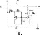
PE单元22产生与施加到数据电极线DL上的视频信号(即,电流信号)对应的光,由此显示与这些视频信号对应的画面。为此,如图3所示,每一个PE单元22包括:发光元件驱动电路30,它用来响应于来自每一条数据电极线DL和栅极线GL的驱动信号而驱动发光元件;发光元件OLED,它连接在发光元件驱动电路30与接地电压源GND之间。
发光元件驱动电路30包括:第一驱动薄膜晶体管(TFT)T1,它连接在供电电压线VDD与发光元件OELD之间;第一开关TFT T3,它连接在奇数栅极线GLo与数据线DL之间;第二开关TFT T4,它连接在第一开关TFT T3与偶数栅极线GL之间;第二驱动TFT T2,它连接在位于第一开关TFT T3与第二开关TFT T4之间的阳极和供电电压线VDD之间,从而关于驱动TFT T1形成一镜像电流电路;存储电容Cst,它连接在位于第一驱动TFT T1与第二驱动TFT T2之间的节点和供电电压线VDD之间。这里,TFT是p型电子金属氧化物半导体场效应晶体管(MOSFET)。The light-emitting
驱动TFT T1的栅极端接至第二驱动TFT T2的栅极端;其源极端接至供电电压线VDD;其漏极端接至发光元件OLED。第二驱动TFT T2的源极端接至供电电压线VDD,其漏极端接至第一开关TFT T3的漏极端和第二开关TFT T4的源极端。The gate terminal of the driving TFT T1 is connected to the gate terminal of the second driving TFT T2; its source terminal is connected to the supply voltage line VDD; its drain terminal is connected to the light emitting element OLED. The source terminal of the second driving TFT T2 is connected to the supply voltage line VDD, and the drain terminal thereof is connected to the drain terminal of the first switching TFT T3 and the source terminal of the second switching TFT T4.
第一开关TFT T3的源极端接至数据电极线DL,其栅极端接至奇数栅极线GLo。第二开关TFT T4的漏极端接至第一驱动TFT T1和第二驱动TFT T2的栅极端以及存储电容Cst。第二开关TFT T4的栅极端接至偶数栅极线GLe。The source terminal of the first switching TFT T3 is connected to the data electrode line DL, and the gate terminal thereof is connected to the odd gate line GLo. The drain terminal of the second switching TFT T4 is connected to the gate terminals of the first driving TFT T1 and the second driving TFT T2 and the storage capacitor Cst. The gate terminal of the second switching TFT T4 is connected to the even-numbered gate line GLe.
这里,第一驱动TFT T1和第二驱动TFT T2以形成一镜像电流的方式彼此连接。这样,假定第一驱动TFT T1和第二驱动TFT T2具有相同的沟道宽度,就将流入第一驱动TFT T1的电流量设定为等于流入第二驱动TFT T2的电流。Here, the first driving TFT T1 and the second driving TFT T2 are connected to each other in such a manner as to form a mirror current. Thus, assuming that the first driving TFT T1 and the second driving TFT T2 have the same channel width, the amount of current flowing into the first driving TFT T1 is set equal to the current flowing into the second driving TFT T2.
以下参照图4中的驱动波形详细描述这样一种发光元件驱动电路30的工作过程。The operation of such a light emitting
以在一预定周期内彼此叠加的方式,分别将具有相同宽度的第一栅极信号SP1和第二栅极信号SP2施加到形成相同水平线的奇数电极线GLo和偶数电极线GLe上。这里,在施加第一栅极信号SP1之前施加第二栅极信号SP2。The first gate signal SP1 and the second gate signal SP2 having the same width are respectively applied to the odd electrode line GLo and the even electrode line GLe forming the same horizontal line in such a manner as to be superimposed on each other within a predetermined period. Here, the second gate signal SP2 is applied before the first gate signal SP1 is applied.
如果提供了第一栅极信号SP1和第二栅极信号SP2,那么第一开关TFT T3和第二开关TFT T4导通。随着第一开关TFT T3和第二开关TFT T4导通,通过第一开关TFT T3和第二开关TFT T4将来自数据电极线DL的视频信号施加到第一驱动TFT T1和第二驱动TFT T2上。此时,供有该视频信号的第一驱动TFT T1和第二驱动TFT T2导通。这里,第一驱动TFT T1响应于施加到其栅极端的视频信号,控制从其源极端(即,VDD)流入其漏极端的电流,从而将其供给发光元件OLED,由此使得发光元件OLED发出与该视频信号对应的光量。If the first gate signal SP1 and the second gate signal SP2 are supplied, the first switching TFT T3 and the second switching TFT T4 are turned on. With the first switching TFT T3 and the second switching TFT T4 turned on, the video signal from the data electrode line DL is applied to the first driving TFT T1 and the second driving TFT T2 through the first switching TFT T3 and the second switching TFT T4 superior. At this time, the first driving TFT T1 and the second driving TFT T2 supplied with the video signal are turned on. Here, the first driving TFT T1 controls the current flowing from its source terminal (i.e., VDD) into its drain terminal in response to a video signal applied to its gate terminal, thereby supplying it to the light emitting element OLED, thereby causing the light emitting element OLED to emit light. The amount of light corresponding to this video signal.
同时,第二驱动TFT T2通过第一开关TFT T3将来自供电电压线VDD的电流id施加到数据电极线DL上。这里,由于第一驱动TFT T1和第二驱动TFT T2形成一镜像电流电路,所以流入第一驱动TFT T1和第二驱动TFT T2中的电流相同。其间,存储电容Cst以对应于流入第二驱动TFT T2的电流Id量的方式存储来自供电电压线VDD的电压。另外,当第一栅极信号SP1和第二栅极信号SP2翻转为“截止”(OFF)信号(例如,零电位)以使第一开关TFT T3和第二开关TFT T4截止时,存储电容Cst利用存储于其中的电压使第一驱动TFT T1导通,由此将与视频信号对应的电流施加到发光元件OEL上。另一方面,由于第二栅极信号SP2在SP1之前翻转为“截止”(OFF)信号,也就是说,在已有技术中,第二开关TFT T4在第一开关TFT T3之前截止,所以可以防止存于存储电容Cst中的电压对外部放电。At the same time, the second driving TFT T2 applies the current id from the power supply voltage line VDD to the data electrode line DL through the first switching TFT T3. Here, since the first driving TFT T1 and the second driving TFT T2 form a mirror current circuit, the currents flowing into the first driving TFT T1 and the second driving TFT T2 are the same. Meanwhile, the storage capacitor Cst stores the voltage from the supply voltage line VDD in a manner corresponding to the amount of current Id flowing into the second driving TFT T2. In addition, when the first gate signal SP1 and the second gate signal SP2 are reversed to "off" (OFF) signals (for example, zero potential) so that the first switch TFT T3 and the second switch TFT T4 are turned off, the storage capacitor Cst The first driving TFT T1 is turned on using the voltage stored therein, thereby applying a current corresponding to the video signal to the light emitting element OEL. On the other hand, since the second gate signal SP2 is turned into an "off" (OFF) signal before SP1, that is to say, in the prior art, the second switch TFT T4 is turned off before the first switch TFT T3, so it can The voltage stored in the storage capacitor Cst is prevented from being discharged to the outside.
实际上,传统的EL显示装置分别将第一栅极信号SP1和第二栅极信号SP2依次施加到奇数栅极线GLo和偶数栅极线GLe上,并且将视频信号施加到数据电极线DL上,由此显示所希望的画面。但是,这样一种传统的EL显示装置具有这样一个问题,即,由于驱动单独一个发光元件OELD需要单独一条水平线上的两条栅极线和四个TFT,所以孔径比很低。此外,这样一种传统的EL显示装置有两个栅极驱动器来驱动奇数栅极线GLo和偶数栅极线GLe,所以导致生产成本很高。Actually, the conventional EL display device respectively applies the first gate signal SP1 and the second gate signal SP2 to the odd gate line GLo and the even gate line GLe in sequence, and applies the video signal to the data electrode line DL. to display the desired screen. However, such a conventional EL display device has a problem that the aperture ratio is low since two gate lines and four TFTs on a single horizontal line are required to drive a single light emitting element OELD. In addition, such a conventional EL display device has two gate drivers to drive the odd gate lines GLo and the even gate lines GLe, thus resulting in a high production cost.
发明内容Contents of the invention
因此,本发明涉及一种电致发光显示装置及其驱动方法,它们基本上避免了因已有技术的局限和缺点带来的一个或者多个问题。Accordingly, the present invention is directed to an electroluminescent display device and method of driving the same that substantially obviate one or more of the problems due to limitations and disadvantages of the related art.
本发明的优点在于提供一种具有高孔径比的电致发光显示装置及其驱动方法。The advantage of the present invention is to provide an electroluminescent display device with a high aperture ratio and a driving method thereof.
本发明的其他特征和优点将在以下的描述中列出,根据该描述,它们的一部分将变得很明显,或者可以通过对本发明的实践学会。本发明的这些目的和其他优点将通过所写的说明书及其权利要求书以及附图中具体指出的结构实现和得到。Additional features and advantages of the invention will be set forth in the description which follows, and in part will be obvious from the description, or may be learned by practice of the invention. The objectives and other advantages of the invention will be realized and attained by the structure particularly pointed out in the written description and claims hereof as well as the appended drawings.
为了实现这些和其他优点,根据本发明的目的,如所具体和概括描述的那样,一种电致发光显示装置例如包括:电致发光元件,它们在栅极线和数据线的交叉部分处排布成矩阵式;一供电电压线,它用来将一驱动电压供给各电致发光元件;驱动电路,它们用来响应于视频信号,控制从供电电压线的驱动电压施加到电致发光元件上的电流;控制电路,它们用来将视频信号施加到驱动电路上,其中一个驱动电路包括:第一驱动电路,它设置在第i条水平线(其中i是整数)上,用来在有一栅极信号施加到第(i-1)条栅极线上时,以响应于第i条栅极线控制的来自控制电路的视频信号,将电流施加到位于第i条水平线上的电致发光元件上;和第二驱动电路,它设置在第(i+1)条水平线上,用来在有一栅极信号施加到第(i+1)条栅极线上时,响应于第i条栅极线控制的来自控制电路的视频信号,将电流施加到位于第(i+1)条水平线上的电致发光元件上。In order to achieve these and other advantages, according to the purpose of the present invention, as specifically and broadly described, an electroluminescent display device includes, for example: electroluminescent elements arranged at the intersection of gate lines and data lines Arranged in a matrix; a supply voltage line, which is used to supply a driving voltage to each electroluminescent element; driving circuits, which are used to control the application of the driving voltage from the supply voltage line to the electroluminescent element in response to a video signal current; control circuits, they are used to apply the video signal to the drive circuit, one of the drive circuits includes: a first drive circuit, which is arranged on the i-th horizontal line (where i is an integer), and is used to connect a gate When the signal is applied to the (i-1)th gate line, a current is applied to the electroluminescent element located on the i-th horizontal line in response to the video signal from the control circuit controlled by the i-th gate line ; and a second drive circuit, which is arranged on the (i+1)th horizontal line, and is used to respond to the i-th gate line when a gate signal is applied to the (i+1)-th gate line Controlled by the video signal from the control circuit, current is applied to the electroluminescence element located on the (i+1)th horizontal line.
这里,控制电路位于第一驱动电路与第二驱动电路之间。Here, the control circuit is located between the first driving circuit and the second driving circuit.
设置在第i条水平线上的第二驱动电路连接到第(i-1)条栅极线上。The second driving circuit provided on the i-th horizontal line is connected to the (i-1)-th gate line.
设置在第(i+1)条水平线上的第一驱动电路连接到第(i+1)条栅极线上。The first driving circuit provided on the (i+1)th horizontal line is connected to the (i+1)th gate line.
第一驱动电路包括:第一驱动薄膜晶体管,它具有连接到供电电压线的源极端和连接到位于第i条水平线上的电致发光元件的漏极端;第二驱动薄膜晶体管,它具有连接到第一驱动薄膜晶体管栅极端的漏极端、连接到控制电路的源极端和连接到第(i-1)条栅极线的栅极端;和一存储电容,它连接在第一驱动薄膜晶体管的源极端与栅极端之间。The first drive circuit includes: a first drive thin film transistor, which has a source terminal connected to a supply voltage line and a drain terminal connected to an electroluminescence element on the i-th horizontal line; a second drive thin film transistor, which has a drain terminal connected to The drain terminal of the gate terminal of the first driving thin film transistor, the source terminal connected to the control circuit and the gate terminal connected to the (i-1) gate line; and a storage capacitor connected to the source of the first driving thin film transistor between extremes and the gate terminal.
第二驱动电路包括:第一驱动薄膜晶体管,它具有连接到供电电压线的源极端和连接到位于第(i+1)条水平线上的电致发光元件的漏极端;第二驱动薄膜晶体管,它具有连接到第一驱动薄膜晶体管栅极端的漏极端、连接到控制电路的源极端和连接到第(i+1)条栅极线的栅极端;和一存储电容,它连接在第一驱动薄膜晶体管的源极端与栅极端之间。The second drive circuit includes: a first drive thin film transistor having a source terminal connected to a supply voltage line and a drain terminal connected to an electroluminescent element located on the (i+1)th horizontal line; a second drive thin film transistor, It has a drain terminal connected to the gate terminal of the first driving thin film transistor, a source terminal connected to the control circuit and a gate terminal connected to the (i+1)th gate line; and a storage capacitor connected to the first driving Between the source terminal and the gate terminal of the thin film transistor.
控制电路包括:第一控制薄膜晶体管,它具有连接到供电电压线的源极端和连接到第二驱动薄膜晶体管源极端的漏极端和栅极端;和第二控制薄膜晶体管,它具有连接到第一控制薄膜晶体管栅极端的漏极端、连接到数据线的源极端和连接到第i条栅极线的栅极端。The control circuit includes: a first control thin film transistor having a source terminal connected to the supply voltage line and a drain terminal and a gate terminal connected to the source terminal of the second driving thin film transistor; and a second control thin film transistor having a source terminal connected to the first The drain terminal of the gate terminal of the control thin film transistor, the source terminal connected to the data line and the gate terminal connected to the ith gate line.
这里,第一控制薄膜晶体管和第二控制薄膜晶体管中的任意一个设置在第i条水平线上,而剩下的那个控制薄膜晶体管设置在第(i+1)条水平线上。Here, any one of the first control thin film transistor and the second control thin film transistor is disposed on the i-th horizontal line, and the remaining control thin film transistor is disposed on the (i+1)-th horizontal line.
这种电致发光显示装置还包括:栅极驱动器,它用来将在两个行周期内有一导通电势的栅极信号施加到栅极线上。The electroluminescent display device further includes a gate driver for applying a gate signal having a turn-on potential for two row periods to the gate line.
这里,在一个行周期内,施加到第i条栅极线上的栅极信号与施加到第(i+1)条栅极线上的栅极信号叠加。Here, in one row period, the gate signal applied to the i-th gate line is superimposed with the gate signal applied to the (i+1)-th gate line.
如果将一栅极信号施加到第(i-1)条和第i条栅极线上,那么连接到第(i-1)条栅极线上的第二驱动薄膜晶体管和连接到第i条栅极线上的第二控制薄膜晶体管导通;随着第二控制薄膜晶体管导通,来自数据线的一个视频信号施加到位于第i条水平线上的第一驱动薄膜晶体管和第一控制薄膜晶体管上。If a gate signal is applied to the (i-1)th and i-th gate lines, then the second drive thin film transistor connected to the (i-1)-th gate line and the i-th The second control thin film transistor on the gate line is turned on; as the second control thin film transistor is turned on, a video signal from the data line is applied to the first drive thin film transistor and the first control thin film transistor on the i-th horizontal line superior.
这里,位于第i条水平线上的第一驱动薄膜晶体管将与视频信号对应的电流施加到设置在第i条水平线上的电致发光元件上。Here, the first driving thin film transistor on the i-th horizontal line applies a current corresponding to the video signal to the electroluminescent element disposed on the i-th horizontal line.
第一控制薄膜晶体管将与来自供电电压线的视频信号对应的电流施加到数据线上。The first control thin film transistor applies current corresponding to the video signal from the supply voltage line to the data line.
这里,与第一控制薄膜晶体管内的电流对应的电压存储在存储电容内。Here, the voltage corresponding to the current in the first control thin film transistor is stored in the storage capacitor.
在本发明的另一方面,一种电致发光显示装置可以例如包括:多个象素,它们排布成矩阵式;多条数据线,它们用来将视频信号施加到各象素上;多条栅极线,它们与数据线交叉,一条栅极线被在该栅极线的上侧和下侧彼此相邻的各象素共用;为每一个象素设置的电致发光元件;供电电压线,它用来将一驱动电压供给各电致发光元件;驱动电路,它们用来响应于视频信号,将与视频信号对应的电流施加到电致发光元件上;和控制电路,它们连接到数据线上,用以将供给数据线的视频信号施加到驱动电路上,其中每一个驱动电路包括:第一驱动电路,它设置在第i条水平线(其中i是整数)上,用来在有一栅极信号施加到第(i-1)条栅极线上时,响应于第i条栅极线控制的来自控制电路的视频信号,将电流施加到位于第i条水平线上的电致发光元件上;和第二驱动电路,它设置在第(i+1)条水平线上,用来在有一栅极信号施加到第(i+1)条栅极线上时,响应于第i条栅极线控制的来自控制电路的视频信号,将电流施加到位于第(i+1)条水平线上的电致发光元件上。In another aspect of the present invention, an electroluminescent display device may include, for example: a plurality of pixels, which are arranged in a matrix; a plurality of data lines, which are used to apply video signals to each pixel; Gate lines crossing the data lines, one gate line shared by pixels adjacent to each other on the upper and lower sides of the gate line; an electroluminescence element provided for each pixel; a power supply voltage lines for supplying a driving voltage to each electroluminescent element; driving circuits for applying a current corresponding to the video signal to the electroluminescent elements in response to the video signal; and control circuits for connecting to the data On the line, it is used to apply the video signal supplied to the data line to the driving circuit, wherein each driving circuit includes: a first driving circuit, which is arranged on the i-th horizontal line (where i is an integer), and is used for When the pole signal is applied to the (i-1)th gate line, a current is applied to the electroluminescent element on the i-th horizontal line in response to the video signal from the control circuit controlled by the i-th gate line ; and a second drive circuit, which is arranged on the (i+1)th horizontal line, and is used to respond to the i-th gate line when a gate signal is applied to the (i+1)-th gate line Controlled by the video signal from the control circuit, current is applied to the electroluminescence element located on the (i+1)th horizontal line.
这种电致发光显示装置还包括:栅极驱动器,它用来将在两个行周期内具有导通电势的栅极信号施加到栅极线上。The electroluminescent display device further includes a gate driver for applying a gate signal having a turn-on potential for two row periods to the gate lines.
这里,在一个行周期内,施加到第i条栅极线(其中i是整数)上的栅极信号与施加到第(i+1)条栅极线上的栅极信号叠加。Here, in one row period, the gate signal applied to the i-th gate line (where i is an integer) is superimposed with the gate signal applied to the (i+1)-th gate line.
这里,控制电路位于第一驱动电路与第二驱动电路之间。Here, the control circuit is located between the first driving circuit and the second driving circuit.
在本发明的另一个方面,一种平板显示装置可以例如包括:多条栅极线,它们包括第N-1、第N和第N+1条栅极线,其中N是整数并且大于1;与栅极线交叉的多条数据线;和第一、第二与第三驱动块,每一个块与至少一条数据线和至少一条栅极线电连接,其中每一个块包括第一驱动电路和第二驱动电路以及以控制电路;其中第N-1条栅极线与第二驱动块的第一驱动电路和第一驱动块的第二驱动电路电连接,第N条栅极线与第二驱动块的控制电路电连接,而第N+1条栅极线与第二驱动块的第二驱动电路和第三驱动块的第一驱动电路电连接。In another aspect of the present invention, a flat panel display device may include, for example: a plurality of gate lines, including N-1th, Nth and N+1th gate lines, wherein N is an integer and greater than 1; A plurality of data lines crossing the gate lines; and first, second and third drive blocks, each block is electrically connected to at least one data line and at least one gate line, wherein each block includes a first drive circuit and The second drive circuit and the control circuit; wherein the N-1th gate line is electrically connected to the first drive circuit of the second drive block and the second drive circuit of the first drive block, and the Nth gate line is connected to the second The control circuit of the driving block is electrically connected, and the N+1th gate line is electrically connected to the second driving circuit of the second driving block and the first driving circuit of the third driving block.
应理解的是,前面总的描述和以下的详细描述是示例和解释性的,意欲用它们提供对所要求保护的本发明的进一步解释。It is to be understood that both the foregoing general description and the following detailed description are exemplary and explanatory and are intended to provide further explanation of the invention as claimed.
附图说明Description of drawings
所包括用来提供对本发明进一步理解并且包括在内构成本说明书一部分的附图示出了本发明的各个实施例,并且连同文字说明一起用来解释本发明的原理。The accompanying drawings, which are included to provide a further understanding of the invention and are incorporated in and constitute a part of this specification, illustrate various embodiments of the invention and together with the description serve to explain the principles of the invention.
这些附图中:In these drawings:
图1是示意性剖视图,它示出了一种已有技术电致发光显示板中有机发光元件的结构;Fig. 1 is a schematic sectional view showing the structure of an organic light-emitting element in a prior art electroluminescent display panel;
图2是一方框图,它示出了一种已有技术电致发光显示板的结构;Fig. 2 is a block diagram showing the structure of a prior art electroluminescent display panel;
图3是图2中所示每一个象素单元PE的等效电路图;Fig. 3 is the equivalent circuit diagram of each pixel unit PE shown in Fig. 2;
图4是施加到图2中所示栅极线上的栅极信号波形图;Fig. 4 is a waveform diagram of a gate signal applied to the gate line shown in Fig. 2;
图5是一方框图,它示出了根据本发明一个实施例的电致发光显示装置的结构;5 is a block diagram showing the structure of an electroluminescent display device according to an embodiment of the present invention;
图6是图5中所示每一个象素单元PE的等效电路图;Fig. 6 is the equivalent circuit diagram of each pixel unit PE shown in Fig. 5;
图7是施加到图5中所示栅极线上的栅极信号的波形图。FIG. 7 is a waveform diagram of gate signals applied to the gate lines shown in FIG. 5. Referring to FIG.
具体实施方式Detailed ways
以下详细描述本发明的一个实施例,其实例示于附图中。DETAILED DESCRIPTION OF THE INVENTION An embodiment of the present invention is described in detail below, examples of which are illustrated in the accompanying drawings.
图5示出了根据本发明一个实施例的有源矩阵型电致发光(EL)显示装置。FIG. 5 shows an active matrix type electroluminescent (EL) display device according to one embodiment of the present invention.
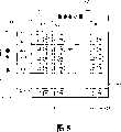
参见图5,这种EL显示装置包括:EL显示板40,它具有排布在栅极GL与数据电极线DL之间每一个交叉部分上的象素(下文简称为“PE”)单元46;栅极驱动器44,它用来驱动栅极线GL;和数据驱动器42,它用来驱动数据电极线DL。Referring to FIG. 5, this EL display device includes: an
栅极线GL连接到位于其上/下部分上的PE单元46上。换句话说,第i条栅极线GLi(其中i是整数)连接到设置在第i条水平线上的PE单元46和设置在第(i+1)条水平线上的PE单元46。这里,第i条栅极线GLi驱动设置在第i条和第(i+1)条水平线上的PE单元46。换句话说,本发明的该实施例使单独一条栅极线GL能够驱动在其上/下部分彼此相邻的PE单元46。这样,与已有技术相比,本发明的该实施例可以减少一半(1/2)的栅极线数目,因此可以确保有高孔径比。此外,由于减少了栅极线GL的数目,所以可以用单独一个栅极驱动器44来驱动EL显示装置并且减小生产成本。The gate line GL is connected to the
如图7所示,栅极驱动器将具有一导通电势的栅极信号依次在两个行周期(2H)内施加到栅极线GL上。这里,在一个行周期(1H)内,施加到第i条栅极线GLi上的栅极信号与施加到第(i-1)条栅极线GLi-1上的栅极信号叠加。As shown in FIG. 7, the gate driver sequentially applies a gate signal having a turn-on potential to the gate line GL for two row periods (2H). Here, in one row period (1H), the gate signal applied to the i-th gate line GLi is superposed with the gate signal applied to the (i-1)-th gate line GLi-1.
数据驱动器42通过数据电极线DL将与一个数据对应的视频信号施加到PE单元46上。这里,在每一个行周期(1H)内,数据驱动器42将每一条水平线的视频信号施加到数据电极线DL上。The
PE单元46发出与施加到数据电极线DL上的视频信号(即,电流信号)对应的光,从而显示画面。为此,如图6所示构造PE单元46。The
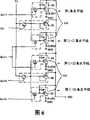
参见图6,根据本发明一个实施例的PE单元46包括:驱动电路50,它用来驱动发光元件OLED;和控制电路52,它用来控制在其上/下部彼此相邻的驱动电路50。这里,在相邻的两个驱动电路50垂直构成受到单独一个控制电路52控制的电路对100或者102(下文称为“驱动电路对”)。控制电路52在连接到其上的单独一条栅极线GL的控制下,控制两个驱动电路50。Referring to FIG. 6, a
驱动电路50配置成使得可以将电流施加到排布成矩阵式的每一个发光元件OLED上。控制电路52设置在每一个驱动电路对100或者102的两个驱动电路50之间,由此控制垂直相邻的驱动电路50。这里,为每一个驱动电路对100和102设置控制电路52,以将包括在一条垂直线内的控制电路52数目设定为驱动电路50数目的一半。The driving
另一方面,在其上下部分彼此相邻并且其间没有设置控制电路52的驱动电路50连接到同一条栅极线上。例如,如果设置在第i条和第(i+1)条水平线上的驱动电路50构成驱动电路对100,而设置在第(i+2)条和第(i+3)条水平线上的驱动电路50构成驱动电路对102,那么位于第(i+1)条水平线和第(i+2)条水平线上的驱动电路50连接到同一条栅极线上。On the other hand, the
为每一个发光元件OLED设置的驱动电路50有两个TFT T1和T2。例如,每一个驱动电路50包括:第一驱动TFT T1,它设置在发光元件OLED与供电电压线VDD之间;第二驱动TFT T2,它设置在第一驱动TFT T1与栅极线GL之间。The
这里,例如在驱动电路对100中的驱动电路50设置在第i条水平线上,第一驱动电路50中的第二驱动TFT T2的栅极端则连接到第(i-1)条栅极线GLi-1上(其中,第(i-1)条栅极线GLi-1还连接到设置在第(i-1)条水平线上的驱动电路50的第二驱动TFT T2上),并且其源极端连接到与其相邻设置的控制电路52上。设置在第i条水平线上的驱动电路50中所包括的第一驱动TFT T1的栅极端连接到第二驱动TFT T2的漏极端,并且其源极端连接到供电电压线VDD上。另外,第一驱动TFT T1的漏极端连接到发光元件OLED1上。存储电容Cst连接在第一驱动TFT T1的源极端与栅极端之间。Here, for example, the driving
另一方面,例如在驱动电路对100中的第二驱动电路50设置在第(i+1)条水平线上,驱动电路50中的第二驱动TFT T2的栅极端连接到第(i+1)条栅极线GLi+1上(其中,第(i+1)条栅极线GLi+1还连接到设置在第(i+2)条水平线上的驱动电路50的第二驱动TFT T2上),并且其源极端连接到与其相邻设置的控制电路52上。设置在第(i+1)条水平线上的驱动电路50中所包括的第一驱动TFT T1的栅极端连接到第二驱动TFT T2的漏极端,并且其源极端连接到供电电压线VDD上。另外,第一驱动TFT T1的漏极端连接到发光元件OLED2上。存储电容Cst连接在第一驱动TFT T1的源极端与栅极端之间。以这种方式,为每一个发光元件OLED设置包括在驱动电路对100和102内的第一TFT T1和第二TFT T2。On the other hand, for example, the
设置在驱动电路对100的两个驱动电路50之间的控制电路52,例如,位于第i条水平线与第(i+1)条水平线之间的控制电路52包括第一控制TFT T3和第二控制TFT T4。这里,以位于不同水平线上的方式设置包括在控制电路52中的两个TFT T3和T4。例如,将第一控制TFT T3设置成位于第i条水平线上,而将第二控制TFT T4设置成位于第(i+1)条水平线上。作为替代,也可以将第一控制TFT T3设置成位于第(i+1)条水平线上,而将第二控制TFT T4设置成位于第i条水平线上。The
第一控制TFT T3的源极端连接到供电电压线VDD上,并且其漏极端和栅极端连接到位于其上/下部处的驱动电路50中所包括的第二驱动TFT T2上。第二控制TFT T4的源极端连接到数据线DL上;其漏极端连接到第一控制TFTT3的漏极端和栅极端上;而其栅极端连接到第i条栅极线GLi上。The source terminal of the first control TFT T3 is connected to the power supply voltage line VDD, and the drain terminal and gate terminal thereof are connected to the second driving TFT T2 included in the driving
以下将参照图7的驱动波形详细描述根据本发明实施例的PE单元46的工作过程。The working process of the
首先,将一栅极信号施加到第(i-1)条栅极线GLi-1上。然后,在一个行周期(1H)内,将与供给第(i-1)条栅极线GLi-1的栅极信号叠加的另一个栅极信号施加到第i条栅极线GLi上。随着一栅极信号施加到第(i-1)条栅极线GLi-1上,位于第i条水平线上的第二驱动TFT T2导通。另外,随着一栅极信号施加到第i条栅极线GLi上,连接到第i条栅极线GLi上的第二控制TFTT4导通。随着第二控制TFT T4和第二驱动TFT T2导通,将来自数据电极线DL的视频信号施加到第一控制TFT T3和第一驱动TFT T1的栅极端。此时,供有该视频信号的第一控制TFT T3和第一驱动TFT T1导通。First, a gate signal is applied to the (i-1)th gate line GLi-1. Then, another gate signal superimposed on the gate signal supplied to the (i-1)th gate line GLi-1 is applied to the i-th gate line GLi within one row period (1H). As a gate signal is applied to the (i-1)th gate line GLi-1, the second driving TFT T2 on the i-th horizontal line is turned on. In addition, as a gate signal is applied to the i-th gate line GLi, the second control TFT T4 connected to the i-th gate line GLi is turned on. With the second control TFT T4 and the second driving TFT T2 turned on, the video signal from the data electrode line DL is applied to the gate terminals of the first control TFT T3 and the first driving TFT T1. At this time, the first control TFT T3 and the first driving TFT T1 supplied with the video signal are turned on.
这里,响应于施加到第一驱动TFT T1栅极端的视频信号,该第一驱动TFTT1控制从其源极端(即,VDD)流入其漏极端的电流,从而将其施加到发光元件OLED1上,由此使发光元件OLED1发出与该视频信号对应的光量。同时,第一控制TFT T3通过第二控制TFT T4将来自供电电压线VDD的电流施加到数据电极线DL上。其间,存储电容Cst以与第一控制TFT T3中电流量相应的方式存储来自供电电压线VDD的电压。这样,当没有施加该视频信号时,存储电容Cst利用存储于其中的电压使第一驱动TFT T1导通,由此将与该视频信号对应的电流施加到发光元件OLED1上。Here, in response to a video signal applied to the gate terminal of the first driving TFT T1, the first driving TFT T1 controls the current flowing from its source terminal (i.e., VDD) into its drain terminal so as to be applied to the light emitting element OLED1, by This causes the light emitting element OLED1 to emit the amount of light corresponding to the video signal. At the same time, the first control TFT T3 applies the current from the supply voltage line VDD to the data electrode line DL through the second control TFT T4. Meanwhile, the storage capacitor Cst stores the voltage from the supply voltage line VDD in a manner corresponding to the amount of current in the first control TFT T3. In this way, when the video signal is not applied, the storage capacitor Cst uses the voltage stored therein to turn on the first driving TFT T1, thereby applying a current corresponding to the video signal to the light emitting element OLED1.
之后,以与施加到第i条栅极线GLi上的栅极信号叠加的方式将另一个栅极信号施加到第(i+1)条栅极线GLi+1上。随着一栅极信号施加到第(i+1)条栅极线GLi+1上,位于第(i+1)条水平线上的第二驱动TFT T2和位于第(i+2)条水平线上的第二驱动TFT T2导通。随着位于第(i+1)条水平线上的第二驱动TFT T2导通,通过位于第(i+1)条水平线上的第二驱动TFT T2,将来自数据电极线DL的视频信号施加到第一驱动TFT T1的栅极端,由此导通第一驱动TFTT1。After that, another gate signal is applied to the (i+1)-th gate line GLi+1 in a manner of being superimposed on the gate signal applied to the i-th gate line GLi. As a gate signal is applied to the (i+1)th gate line GLi+1, the second driving TFT T2 positioned on the (i+1)th horizontal line and the (i+2)th horizontal line The second driving TFT T2 is turned on. As the second driving TFT T2 on the (i+1)th horizontal line is turned on, the video signal from the data electrode line DL is applied to the The gate terminal of the first driving TFT T1 is turned on, thereby turning on the first driving TFT T1.
此时,响应于施加到位于第(i+1)条水平线上的第一驱动TFT T1的栅极端的视频信号,该第一驱动TFT T1控制从其源极端(即,VDD)流入其漏极端的电流,从而将其施加到发光元件OLED2上,由此使发光元件OLED2发出与该视频信号对应的光量。同时,通过第二控制TFT T4,第一控制TFT T3将根据一视频信号而变得不同的来自供电电压线VDD的电流施加到数据电极线DL上。其间,存储电容Cst以与第一控制TFT T3中电流量相应的方式存储来自供电电压线VDD的电压。这样,当没有施加该视频信号时,存储电容Cst利用存储于其中的电压使第一驱动TFT T1导通,由此将与该视频信号对应的电流施加到发光元件OLED2上。At this time, in response to a video signal applied to the gate terminal of the first driving TFT T1 located on the (i+1)th horizontal line, the first driving TFT T1 controls the flow from its source terminal (i.e., VDD) to its drain terminal. The current is applied to the light-emitting element OLED2, thereby causing the light-emitting element OLED2 to emit light corresponding to the video signal. Meanwhile, the first control TFT T3 applies a current from the supply voltage line VDD, which becomes different according to a video signal, to the data electrode line DL through the second control TFT T4. Meanwhile, the storage capacitor Cst stores the voltage from the supply voltage line VDD in a manner corresponding to the amount of current in the first control TFT T3. Thus, when the video signal is not applied, the storage capacitor Cst uses the voltage stored therein to turn on the first driving TFT T1, thereby applying a current corresponding to the video signal to the light emitting element OLED2.
其间,虽然施加到第(i+1)条栅极线GLi+1上的栅极信号使位于第(i+2)条水平线上的第二驱动TFT T2导通,但是视频信号无法到达位于第(i+2)条水平线上的发光元件OLED3,因为位于驱动电路对102之间的第二控制TFT T4截止。这样,此时,位于第(i+2)条水平线上的发光元件OLED3不发光。Meanwhile, although the gate signal applied to the (i+1)th gate line GLi+1 turns on the second driving TFT T2 located on the (i+2)th horizontal line, the video signal cannot reach the second driving TFT T2 located on the (i+2)th horizontal line. The light emitting elements OLED3 on the (i+2) horizontal lines are turned off because the second control TFT T4 located between the pair of driving
之后,以与施加到第(i+1)条栅极线GLi+1上的栅极信号叠加的方式将另一个栅极信号施加到第(i+2)条栅极线GLi+2上。随着一栅极信号施加到第(i+2)条栅极线GLi+2上,连接到第(i+2)条栅极线GLi+2上的第二驱动TFT T4导通。随着第二驱动TFT T4导通,来自数据电极线DL的视频信号使连接到第二控制TFT T4上的第一控制TFT T3和位于第(i+2)条水平线上的第一驱动TFTT1导通。After that, another gate signal is applied to the (i+2)th gate line GLi+2 in a manner of being superimposed on the gate signal applied to the (i+1)th gate line GLi+1. As a gate signal is applied to the (i+2)th gate line GLi+2, the second driving TFT T4 connected to the (i+2)th gate line GLi+2 is turned on. With the second driving TFT T4 turned on, the video signal from the data electrode line DL makes the first control TFT T3 connected to the second control TFT T4 and the first driving TFT T1 on the (i+2)th horizontal line conduct. Pass.
此时,响应于施加到位于第(i+2)条水平线上的第一驱动TFT T1的栅极端上的视频信号,该第一驱动TFT T1控制从其源极端(即,VDD)流入其漏极端的电流,从而将其施加到发光元件OLED3上,由此使发光元件OLED3发出对应于该视频信号的光量。同时,通过第二控制TFT T4,第一控制TFT T3将来自供电电压线VDD的电流施加到数据电极线DL上。其间,存储电容Cst以与第一控制TFT T3中电流量相应的方式存储来自供电电压线VDD的电压。这样,当没有施加该视频信号时,存储电容Cst利用存储于其中的电压使第一驱动TFT T1导通,由此将与该视频信号对应的电流施加到发光元件OLED3上。实际上,本EL显示装置重复了上述过程,由此显示所期望的画面。At this time, in response to a video signal applied to the gate terminal of the first driving TFT T1 located on the (i+2)th horizontal line, the first driving TFT T1 controls the flow from its source terminal (i.e., VDD) to its drain. An extreme current is applied to the light emitting element OLED3, thereby causing the light emitting element OLED3 to emit a light amount corresponding to the video signal. At the same time, the first control TFT T3 applies the current from the supply voltage line VDD to the data electrode line DL through the second control TFT T4. Meanwhile, the storage capacitor Cst stores the voltage from the supply voltage line VDD in a manner corresponding to the amount of current in the first control TFT T3. In this way, when the video signal is not applied, the storage capacitor Cst uses the voltage stored therein to turn on the first driving TFT T1, thereby applying a current corresponding to the video signal to the light emitting element OLED3. Actually, the present EL display device repeats the above process, thereby displaying a desired screen.
这样一种EL显示装置提供单独一个控制电路,该控制电路位于其上/下部彼此相邻的驱动电路对之间,并且控制位于上/下两侧的驱动电路,同时由单独一条栅极线控制该控制电路,从而使它能够减少栅极线的数目。换句话说,由于设置在驱动电路对上侧的驱动电路与设置在前一条水平线上的驱动电路都连接到同一条栅极线上,而设置在驱动电路对下侧的驱动电路与设置在下一条水平线上的驱动电路都连接到同一条栅极线上,所以可以使栅极线的数目最少,由此提高孔径比。此外,为排布成矩阵式的每一个发光元件设置三个TFT(即,在驱动电路上的两个TFT和在控制电路上的一个TFT),可以更大地提高孔径比。Such an EL display device provides a single control circuit which is located between a pair of driving circuits adjacent to each other at its upper/lower portions and which controls the driving circuits located at both upper/lower sides while being controlled by a single gate line The control circuit thus makes it possible to reduce the number of gate lines. In other words, since the driver circuit arranged on the upper side of the pair of driver circuits is connected to the same gate line as the driver circuit arranged on the previous horizontal line, the driver circuit arranged on the lower side of the pair of driver circuits is connected to the same gate line as the driver circuit arranged on the next horizontal line. The drive circuits on the horizontal lines are all connected to the same gate line, so the number of gate lines can be minimized, thereby improving the aperture ratio. In addition, providing three TFTs (ie, two TFTs on the driving circuit and one TFT on the control circuit) for each light emitting element arranged in a matrix can further increase the aperture ratio.
如上所述,根据本发明,栅极线控制位于上/下侧的象素单元,从而能够减少栅极线的数目,由此提高孔径比。此外,根据本发明,为每一个象素单元都包括三个TFT,从而与已有技术相比,可以更大地提高孔径比。此外,根据本发明,减少的栅极线的数目,从而可以用单独一个栅极驱动器将一个栅极信号施加到所有栅极线上,由此降低了生产成本。As described above, according to the present invention, the gate lines control the pixel units on the upper/lower sides, so that the number of gate lines can be reduced, thereby improving the aperture ratio. In addition, according to the present invention, three TFTs are included for each pixel unit, so that the aperture ratio can be greatly improved compared with the prior art. Furthermore, according to the present invention, the number of gate lines is reduced so that a single gate driver can be used to apply one gate signal to all gate lines, thereby reducing production costs.
显然,对于本领域的那些技术人员来说,在不脱离本发明的精神或者范围的基础上,本发明可以做各种修改和变换。这样,假定对本发明的这些修改和变换落在所附权利要求书及其等同物的范围内,都将被本发明所涵盖。It is obvious to those skilled in the art that various modifications and changes can be made to the present invention without departing from the spirit or scope of the present invention. Thus, it is assumed that the modifications and changes of the present invention fall within the scope of the appended claims and their equivalents, and shall be covered by the present invention.
Claims (18)
Applications Claiming Priority (2)
| Application Number | Priority Date | Filing Date | Title |
|---|---|---|---|
| KR1020030083944 | 2003-11-25 | ||
| KR1020030083944AKR100607513B1 (en) | 2003-11-25 | 2003-11-25 | Electro-luminescence display and its driving method |
Publications (2)
| Publication Number | Publication Date |
|---|---|
| CN1622166A CN1622166A (en) | 2005-06-01 |
| CN100378779Ctrue CN100378779C (en) | 2008-04-02 |
Family
ID=34588042
Family Applications (1)
| Application Number | Title | Priority Date | Filing Date |
|---|---|---|---|
| CNB2004100426424AExpired - LifetimeCN100378779C (en) | 2003-11-25 | 2004-05-28 | Electroluminescence display device and driving method thereof |
Country Status (5)
| Country | Link |
|---|---|
| US (1) | US7903051B2 (en) |
| JP (1) | JP4210244B2 (en) |
| KR (1) | KR100607513B1 (en) |
| CN (1) | CN100378779C (en) |
| TW (1) | TWI274311B (en) |
Cited By (1)
| Publication number | Priority date | Publication date | Assignee | Title |
|---|---|---|---|---|
| CN104517565A (en)* | 2013-09-27 | 2015-04-15 | 昆山国显光电有限公司 | Organic light-emitting displayer pixel circuit, driving method and display device thereof |
Families Citing this family (12)
| Publication number | Priority date | Publication date | Assignee | Title |
|---|---|---|---|---|
| KR100583135B1 (en)* | 2004-06-08 | 2006-05-23 | 삼성에스디아이 주식회사 | Electroluminescent display |
| KR100806814B1 (en)* | 2006-06-23 | 2008-02-25 | 엘지.필립스 엘시디 주식회사 | Driving device of organic EL element |
| JP5157317B2 (en)* | 2007-08-21 | 2013-03-06 | ソニー株式会社 | Method for driving organic electroluminescence light emitting unit and organic electroluminescence display device |
| JP4655085B2 (en) | 2007-12-21 | 2011-03-23 | ソニー株式会社 | Display device and electronic device |
| US20090219233A1 (en)* | 2008-03-03 | 2009-09-03 | Park Yong-Sung | Organic light emitting display and method of driving the same |
| US8497828B2 (en)* | 2009-11-12 | 2013-07-30 | Ignis Innovation Inc. | Sharing switch TFTS in pixel circuits |
| JP4655160B2 (en)* | 2009-12-11 | 2011-03-23 | ソニー株式会社 | Display device and electronic device |
| KR101064471B1 (en)* | 2010-03-17 | 2011-09-15 | 삼성모바일디스플레이주식회사 | Organic light emitting display |
| KR101812176B1 (en)* | 2011-05-20 | 2017-12-27 | 삼성디스플레이 주식회사 | Organc light emitting diode display |
| CN103268753A (en)* | 2013-05-28 | 2013-08-28 | 上海中科高等研究院 | AMOLED driving circuit shared by scanning lines and its driving method |
| KR102527222B1 (en)* | 2015-08-10 | 2023-05-02 | 삼성디스플레이 주식회사 | Display apparatus |
| CN111968584A (en)* | 2020-08-06 | 2020-11-20 | 武汉华星光电技术有限公司 | Display panel and display device |
Citations (3)
| Publication number | Priority date | Publication date | Assignee | Title |
|---|---|---|---|---|
| US20010050662A1 (en)* | 2000-03-17 | 2001-12-13 | Atsushi Kota | Image display device and drive method thereof |
| JP2002214645A (en)* | 2001-01-22 | 2002-07-31 | Matsushita Electric Ind Co Ltd | Active matrix display device |
| CN1418043A (en)* | 2001-11-03 | 2003-05-14 | Lg.菲利浦Lcd株式会社 | electroluminescent panel |
Family Cites Families (8)
| Publication number | Priority date | Publication date | Assignee | Title |
|---|---|---|---|---|
| KR100566813B1 (en) | 2000-02-03 | 2006-04-03 | 엘지.필립스 엘시디 주식회사 | Electroluminescence cell driving circuit |
| TW521256B (en)* | 2000-05-18 | 2003-02-21 | Semiconductor Energy Lab | Electronic device and method of driving the same |
| JP4831889B2 (en)* | 2000-06-22 | 2011-12-07 | 株式会社半導体エネルギー研究所 | Display device |
| US6690034B2 (en)* | 2000-07-31 | 2004-02-10 | Semiconductor Energy Laboratory Co., Ltd. | Light emitting device |
| JP3593982B2 (en) | 2001-01-15 | 2004-11-24 | ソニー株式会社 | Active matrix type display device, active matrix type organic electroluminescence display device, and driving method thereof |
| JP2002244617A (en)* | 2001-02-15 | 2002-08-30 | Sanyo Electric Co Ltd | Organic el pixel circuit |
| JP3743387B2 (en) | 2001-05-31 | 2006-02-08 | ソニー株式会社 | Active matrix display device, active matrix organic electroluminescence display device, and driving method thereof |
| KR100910562B1 (en)* | 2002-12-17 | 2009-08-03 | 삼성전자주식회사 | Drive of display device |
- 2003
- 2003-11-25KRKR1020030083944Apatent/KR100607513B1/ennot_activeExpired - Lifetime
- 2004
- 2004-04-16USUS10/825,357patent/US7903051B2/enactiveActive
- 2004-05-26TWTW093114963Apatent/TWI274311B/ennot_activeIP Right Cessation
- 2004-05-28CNCNB2004100426424Apatent/CN100378779C/ennot_activeExpired - Lifetime
- 2004-06-29JPJP2004192103Apatent/JP4210244B2/ennot_activeExpired - Lifetime
Patent Citations (3)
| Publication number | Priority date | Publication date | Assignee | Title |
|---|---|---|---|---|
| US20010050662A1 (en)* | 2000-03-17 | 2001-12-13 | Atsushi Kota | Image display device and drive method thereof |
| JP2002214645A (en)* | 2001-01-22 | 2002-07-31 | Matsushita Electric Ind Co Ltd | Active matrix display device |
| CN1418043A (en)* | 2001-11-03 | 2003-05-14 | Lg.菲利浦Lcd株式会社 | electroluminescent panel |
Cited By (2)
| Publication number | Priority date | Publication date | Assignee | Title |
|---|---|---|---|---|
| CN104517565A (en)* | 2013-09-27 | 2015-04-15 | 昆山国显光电有限公司 | Organic light-emitting displayer pixel circuit, driving method and display device thereof |
| CN104517565B (en)* | 2013-09-27 | 2017-09-29 | 昆山国显光电有限公司 | Image element circuit, driving method and its display device of OLED |
Also Published As
| Publication number | Publication date |
|---|---|
| CN1622166A (en) | 2005-06-01 |
| US20050110718A1 (en) | 2005-05-26 |
| JP2005157277A (en) | 2005-06-16 |
| KR100607513B1 (en) | 2006-08-02 |
| US7903051B2 (en) | 2011-03-08 |
| TW200517995A (en) | 2005-06-01 |
| KR20050050242A (en) | 2005-05-31 |
| TWI274311B (en) | 2007-02-21 |
| JP4210244B2 (en) | 2009-01-14 |
Similar Documents
| Publication | Publication Date | Title |
|---|---|---|
| US6864637B2 (en) | Organic electro luminescence device and method for driving the same | |
| US7365714B2 (en) | Data driving apparatus and method of driving organic electro luminescence display panel | |
| US6858992B2 (en) | Organic electro-luminescence device and method and apparatus for driving the same | |
| KR101117731B1 (en) | Pixel circuit, and organic light emitting display, and driving method thereof | |
| KR101030002B1 (en) | Pixel circuit and organic light emitting display device using same | |
| KR100405877B1 (en) | Organic light emitting diode display and operating method of driving the same | |
| KR100528692B1 (en) | Aging Circuit For Organic Electroluminescence Device And Method Of Driving The same | |
| KR20060106748A (en) | Electro-luminescence display and its driving method | |
| JP2007004114A (en) | Organic light emitting diode driving circuit, organic light emitting diode display device, and driving method of organic light emitting diode display device | |
| CN103778886A (en) | Display apparatus | |
| JP2006114876A (en) | Light emitting display device and light emitting display panel | |
| CN100407268C (en) | Electroluminescent display device | |
| CN100378779C (en) | Electroluminescence display device and driving method thereof | |
| US7486261B2 (en) | Electro-luminescent display device | |
| JP2005122183A (en) | Electro-luminescence display device | |
| CN118447796A (en) | Timing control device and driving method thereof, display panel, and display device | |
| US7808454B2 (en) | Display device and method of driving the same | |
| KR20070119200A (en) | Organic light emitting diode display | |
| JP4209361B2 (en) | EL display panel driving device and driving method, and EL display device manufacturing method | |
| KR100568595B1 (en) | Electro-luminescence display | |
| KR100538331B1 (en) | Electro luminescence display device | |
| KR20070028752A (en) | EL display device and driving method |
Legal Events
| Date | Code | Title | Description |
|---|---|---|---|
| C06 | Publication | ||
| PB01 | Publication | ||
| C10 | Entry into substantive examination | ||
| SE01 | Entry into force of request for substantive examination | ||
| C14 | Grant of patent or utility model | ||
| GR01 | Patent grant | ||
| C56 | Change in the name or address of the patentee | Owner name:LG DISPLAY CO., LTD. Free format text:FORMER NAME OR ADDRESS: LG. PHILIP LCD CO., LTD. | |
| CP01 | Change in the name or title of a patent holder | Address after:Seoul, South Kerean Patentee after:LG DISPLAY Co.,Ltd. Address before:Seoul, South Kerean Patentee before:LG.Philips LCD Co.,Ltd. | |
| CX01 | Expiry of patent term | Granted publication date:20080402 | |
| CX01 | Expiry of patent term |