CN100377210C - Magnetic recording medium, manufacturing method thereof, and magnetic recording device - Google Patents
Magnetic recording medium, manufacturing method thereof, and magnetic recording deviceDownload PDFInfo
- Publication number
- CN100377210C CN100377210CCNB2005100600872ACN200510060087ACN100377210CCN 100377210 CCN100377210 CCN 100377210CCN B2005100600872 ACNB2005100600872 ACN B2005100600872ACN 200510060087 ACN200510060087 ACN 200510060087ACN 100377210 CCN100377210 CCN 100377210C
- Authority
- CN
- China
- Prior art keywords
- mentioned
- magnetic
- mark
- magnetic recording
- signal section
- Prior art date
- Legal status (The legal status is an assumption and is not a legal conclusion. Google has not performed a legal analysis and makes no representation as to the accuracy of the status listed.)
- Expired - Fee Related
Links
Images


Classifications
- G—PHYSICS
- G11—INFORMATION STORAGE
- G11B—INFORMATION STORAGE BASED ON RELATIVE MOVEMENT BETWEEN RECORD CARRIER AND TRANSDUCER
- G11B5/00—Recording by magnetisation or demagnetisation of a record carrier; Reproducing by magnetic means; Record carriers therefor
- G11B5/48—Disposition or mounting of heads or head supports relative to record carriers ; arrangements of heads, e.g. for scanning the record carrier to increase the relative speed
- G11B5/58—Disposition or mounting of heads or head supports relative to record carriers ; arrangements of heads, e.g. for scanning the record carrier to increase the relative speed with provision for moving the head for the purpose of maintaining alignment of the head relative to the record carrier during transducing operation, e.g. to compensate for surface irregularities of the latter or for track following
- G11B5/596—Disposition or mounting of heads or head supports relative to record carriers ; arrangements of heads, e.g. for scanning the record carrier to increase the relative speed with provision for moving the head for the purpose of maintaining alignment of the head relative to the record carrier during transducing operation, e.g. to compensate for surface irregularities of the latter or for track following for track following on disks
- G11B5/59633—Servo formatting
- G—PHYSICS
- G11—INFORMATION STORAGE
- G11B—INFORMATION STORAGE BASED ON RELATIVE MOVEMENT BETWEEN RECORD CARRIER AND TRANSDUCER
- G11B5/00—Recording by magnetisation or demagnetisation of a record carrier; Reproducing by magnetic means; Record carriers therefor
- G11B5/84—Processes or apparatus specially adapted for manufacturing record carriers
- G11B5/855—Coating only part of a support with a magnetic layer
- G—PHYSICS
- G11—INFORMATION STORAGE
- G11B—INFORMATION STORAGE BASED ON RELATIVE MOVEMENT BETWEEN RECORD CARRIER AND TRANSDUCER
- G11B5/00—Recording by magnetisation or demagnetisation of a record carrier; Reproducing by magnetic means; Record carriers therefor
- G11B5/86—Re-recording, i.e. transcribing information from one magnetisable record carrier on to one or more similar or dissimilar record carriers
- G11B5/865—Re-recording, i.e. transcribing information from one magnetisable record carrier on to one or more similar or dissimilar record carriers by contact "printing"
Landscapes
- Magnetic Record Carriers (AREA)
- Manufacturing Of Magnetic Record Carriers (AREA)
- Recording Or Reproducing By Magnetic Means (AREA)
- Moving Of The Head To Find And Align With The Track (AREA)
Abstract
Description
Translated fromChinese技术领域technical field
本发明涉及磁记录介质、采用压印光刻法(imprint lithography)的该磁记录介质的制造方法,以及使用该磁记录介质的磁记录装置。The present invention relates to a magnetic recording medium, a method of manufacturing the magnetic recording medium using imprint lithography, and a magnetic recording device using the magnetic recording medium.
背景技术Background technique
在磁记录装置中,伴随着大容量化的要求,必须增加磁记录介质的记录密度。在具有高记录密度的磁记录介质中,在通过磁头向某磁道记录数据时,对邻接的磁道上已记录的数据产生不良影响的可能性增大。为了解决该问题,提出了一种利用在磁道宽度方向上互相物理分离的磁性膜来形成磁道的磁记录介质(分离磁道介质:discrete trackmedia)(例如参见日本专利申请 特开昭62-256225号公报)。In a magnetic recording device, it is necessary to increase the recording density of a magnetic recording medium in response to a demand for a larger capacity. In a magnetic recording medium having a high recording density, when data is recorded on a certain track by a magnetic head, there is an increased possibility of adversely affecting data already recorded on an adjacent track. In order to solve this problem, a magnetic recording medium (separated track media: discrete trackmedia) that forms a track by using magnetic films that are physically separated from each other in the track width direction has been proposed (for example, see Japanese Patent Application Laid-Open No. 62-256225 ).
另外,在磁记录装置中,从磁记录介质的伺服区中读出伺服数据以进行磁头定位。在现有的磁记录介质中,通过利用伺服磁道写入器在磁性膜上进行磁记录,来形成伺服区。与此相比,在分离磁道介质中,最好是处理磁性膜以形成伺服区内的伺服标记,以及也形成分离磁道的图形。这种磁记录介质即所谓图形介质,最好是利用压印光刻法来进行制造。这里,若磁性图形的尺寸为小于等于500nm,则很难用光刻法来加工磁性膜。若利用电子束刻蚀,则能够形成尺寸小于等于500nm的微细结构,但由于扫描速度慢,因而生产能力较低。与此相比,压印光刻法则具有能够在高生产能力下制作图形介质的优点。Also, in a magnetic recording apparatus, servo data is read out from a servo area of a magnetic recording medium to perform head positioning. In a conventional magnetic recording medium, a servo area is formed by performing magnetic recording on a magnetic film with a servo track writer. In contrast, in split track media, it is preferable to process the magnetic film to form servo marks in the servo area, and also to form the pattern of the split tracks. Such magnetic recording media, so-called pattern media, are preferably produced by imprint lithography. Here, if the size of the magnetic pattern is 500nm or less, it is difficult to process the magnetic film by photolithography. If electron beam etching is used, a fine structure with a size of 500nm or less can be formed, but the throughput is low due to the slow scanning speed. In contrast, imprint lithography has the advantage of being able to produce graphic media at high throughput.
下面说明利用压印光刻法来制造磁记录介质(图形介质)的方法。首先,例如用以下方法,来制作实质上具有与磁记录介质上的磁性膜的图形相反图形的凸部的压模。在原盘上涂敷电子束抗蚀剂,利用电子束来扫描预定的图形,进行显影,形成电子束抗蚀剂的凹凸图形。对形成了电子束抗蚀剂的凹凸图形的原盘进行电铸处理,对通过电铸而形成的金属盘进行剥离,制作出压模。然后,例如用以下的压印光刻法来制作磁记录介质。在基片上制作磁性膜,涂敷抗蚀剂。把压模按压到抗蚀剂上,使压模表面的凹凸转印到抗蚀剂表面上,拆下压模后,以转印了凹凸的抗蚀剂作为掩模来加工磁性膜。这样就制造出形成有所需磁性膜图形的磁记录介质(图形介质)。Next, a method of manufacturing a magnetic recording medium (pattern medium) by imprint lithography will be described. First, for example, a stamper having protrusions in a pattern substantially opposite to that of the magnetic film on the magnetic recording medium is produced by the following method. Coating electron beam resist on the original disk, using electron beam to scan a predetermined pattern, and developing it to form the concave-convex pattern of electron beam resist. Electroforming was performed on the original plate on which the concave-convex pattern of the electron beam resist was formed, and the metal plate formed by electroforming was peeled off to produce a stamper. Then, for example, a magnetic recording medium is produced by the following imprint lithography method. Make a magnetic film on the substrate and apply a resist. Press the stamper onto the resist to transfer the unevenness on the surface of the stamper to the resist surface. After removing the stamper, the resist with the unevenness transferred is used as a mask to process the magnetic film. Thus, a magnetic recording medium (patterned medium) formed with a desired magnetic film pattern is produced.
若采用上述压印光刻法,则不但能够将利用电子束刻蚀法制作的压模多次连续用于压印工序,而且压印工序的生产能力提高,因此能够降低介质的制造成本。并且,由于伺服区的磁性标记和数据区的分离磁道成批地形成,因此可望提高伺服区和分离磁道的位置精度。而且,为了提高了记录密度,适用于垂直磁记录介质的制造也是有利的。According to the above-mentioned imprint lithography method, not only can the stamper produced by the electron beam etching method be continuously used in the imprint process multiple times, but also the productivity of the imprint process can be improved, so that the production cost of the medium can be reduced. Also, since the magnetic marks of the servo zone and the separate tracks of the data zone are formed in batches, it is expected to improve the positional accuracy of the servo zone and the separate tracks. Furthermore, in order to increase the recording density, it is also advantageous to be applicable to the manufacture of perpendicular magnetic recording media.
但是,可以看出,在利用压印光刻法来制作磁记录介质的情况下,伺服区的图形使形成的磁性膜厚度产生偏移,其结果是存在着读写变得不稳定的问题。However, it can be seen that when the magnetic recording medium is produced by imprint lithography, the pattern of the servo region deviates the thickness of the formed magnetic film, and as a result, there is a problem that reading and writing becomes unstable.
发明内容Contents of the invention
根据本发明的一种方式的磁记录介质,具有:包含前同步信号区和色同步信号区并具有磁性膜的标记的伺服区;以及具有上述磁性膜的分离磁道的数据区;上述色同步信号区包括信号部和非信号部,上述信号部包括在磁道方向上以周期性的图形形成的上述磁性膜的第一标记,上述非信号部包括上述磁性膜的第二标记,该第二标记具有与上述信号部中的上述第一标记的图形不同的图形。A magnetic recording medium according to an aspect of the present invention has: a servo area including a preamble area and a color burst area and a mark having a magnetic film; a data area having separate tracks of the magnetic film; the color burst signal The area includes a signal portion including a first mark of the above-mentioned magnetic film formed in a periodic pattern in the track direction, and a non-signal portion including a second mark of the above-mentioned magnetic film having A pattern different from that of the first mark in the signal portion.
根据本发明的另一方式的磁记录介质的制造方法为,在基片上沉积磁性膜,在上述磁性膜上涂敷抗蚀剂;将一压模按压到上述抗蚀剂上,以压印一凹凸图形,该凹凸图形对应于上述磁记录介质的上述伺服区和上述数据区的上述标记的图形;以及使用压印后的抗蚀剂作为掩模对上述磁性膜进行处理。A method of manufacturing a magnetic recording medium according to another aspect of the present invention comprises depositing a magnetic film on a substrate, coating a resist on the magnetic film, and pressing a stamper onto the resist to imprint a magnetic film. a concavo-convex pattern corresponding to the pattern of the above-mentioned mark in the above-mentioned servo area and the above-mentioned data area of the above-mentioned magnetic recording medium; and processing the above-mentioned magnetic film using the resist after imprinting as a mask.
根据本发明又一方式的磁记录装置,具有:上述磁记录介质;以及对上述磁记录介质进行读写的磁头。A magnetic recording device according to still another aspect of the present invention includes: the above-mentioned magnetic recording medium; and a magnetic head for reading and writing to the above-mentioned magnetic recording medium.
附图说明Description of drawings
图1A和1B是用压印光刻法进行制造的分离磁道介质的平面图。1A and 1B are plan views of split track media fabricated by imprint lithography.
图2A~2D是用于说明制造图1的分离磁道介质时可能产生的问题的断面图。2A to 2D are cross-sectional views illustrating problems that may arise when manufacturing the split-track medium of FIG. 1 .
图3A和3B是用于说明制造图1的分离磁道介质时可能产生的问题的断面图。3A and 3B are cross-sectional views for explaining problems that may arise in manufacturing the split-track medium of FIG. 1. FIG.
图4是根据第1实施方式的磁记录介质的平面图。4 is a plan view of the magnetic recording medium according to the first embodiment.
图5是根据第2实施方式的磁记录介质的色同步信号区的平面图。5 is a plan view of a burst area of a magnetic recording medium according to a second embodiment.
图6是根据第3实施方式的磁记录介质的色同步信号区的平面图。Fig. 6 is a plan view of a burst area of a magnetic recording medium according to a third embodiment.
图7A~7G是表示根据本发明实施方式的磁记录介质的制造方法的断面图。7A to 7G are cross-sectional views illustrating a method of manufacturing a magnetic recording medium according to an embodiment of the present invention.
图8A是具有图4所示的磁性标记的磁性膜的断面图。FIG. 8A is a cross-sectional view of a magnetic film having the magnetic marker shown in FIG. 4 .
图8B是具有图1A所示的磁性标记的磁性膜的断面图。Fig. 8B is a cross-sectional view of a magnetic film having the magnetic mark shown in Fig. 1A.
图9A~9G是表示根据本发明的另一实施方式的磁记录介质的制造方法的断面图。9A to 9G are cross-sectional views illustrating a method of manufacturing a magnetic recording medium according to another embodiment of the present invention.
图10A是与图4相对应的基片图形制作的分离磁道介质的基片的断面图。Fig. 10A is a cross-sectional view of a substrate of a split-track medium fabricated with a substrate pattern corresponding to Fig. 4 .
图10B是与图1A相对应的基片图形制作的分离磁道介质的基片的断面图。Fig. 10B is a cross-sectional view of a substrate of a split-track medium fabricated with a substrate pattern corresponding to that of Fig. 1A.
图11是根据本发明实施方式的磁记录介质的斜视图。Fig. 11 is a perspective view of a magnetic recording medium according to an embodiment of the present invention.
具体实施方式Detailed ways
以下参照附图,详细说明根据本发明实施方式的磁记录介质,同时也对与本发明相对比的技术进行说明。Hereinafter, a magnetic recording medium according to an embodiment of the present invention will be described in detail with reference to the drawings, and a technology in comparison with the present invention will also be described.
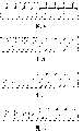
图1A和1B中表示假定用压印光刻法进行制造的磁记录介质(分离磁道介质)的平面图。如图1A和1B所示,这些磁记录介质具有:形成有磁性膜标记的伺服区1,和形成有磁性膜的分离磁道的数据区2。伺服区1包括前同步信号区(preamble region)11、地址区12和色同步信号区(burst region)(定位色同步信号区)13。色同步信号区13有两种情况:一种为如图1A所示,由磁性膜的矩形标记构成;另一种为如图1B所示,由磁性膜中的矩形孔标记构成。但是,在磁记录装置中的图1A的介质和图1B的介质的色同步信号区的信号图形的功能是相同的。为了方便起见,在本说明书中,将图1A的色同步信号图形称为标记型、将图1B的色同步信号图形称为孔型。而且,在磁性标记之间的凹部中,既可以填充非磁性膜,也可以作为空隙。以下说明在磁性标记之间的凹部内填充非磁性膜的情况。另外,在垂直磁记录介质中,磁性标记预先在垂直方向上被磁化。A plan view of a magnetic recording medium (separated track medium) assumed to be manufactured by imprint lithography is shown in FIGS. 1A and 1B. As shown in FIGS. 1A and 1B, these magnetic recording media have a servo area 1 formed with magnetic film marks, and a
前同步信号区11用于与地址区12和色同步信号区13相比,先被磁头50读出,并对信号放大器的放大率进行调整,使振幅达到一定。前同步信号区11形成的图形是并排了在磁道宽度方向(盘的半径方向)上延伸的多个磁性膜的线状标记,使得无论磁头50在哪个磁道位置上均能够获得同样的信号。The
地址区12具有磁道数据和扇区数据。磁道数据为葛莱编码(graycode),使得即使在查找中也能够由磁头50进行读出。The
色同步信号区13是为了使磁头50向预定的磁道中心移动而设置的。色同步信号区13包括信号部13a和非信号部13b。图1A中的信号部13a为,磁性膜的矩形标记以及其间的用非磁性膜填充的空间沿磁道方向(盘的圆周方向)按等间隔形成。图1A中的非信号部13b没有磁性标记,仅由非磁性膜构成。图1B中的信号部13a和图1A中的相同。另一方面,图1B中的非信号部13b仅由磁性膜构成。图1A或1B的色同步信号区13具有和利用伺服磁道写入器进行磁记录的现有的磁记录介质中的色同步信号区相同的图形,在信号部13a中包括距离磁道中心的相对位置互不相同的色同步信号A~色同步信号D。当磁头50对色同步信号区13进行追迹时,再现信号强度根据磁头50距离磁道中心的偏移而变化。也就是说,若磁头50的中心和磁道的中心一致,则由色同步信号A和色同步信号B获得的信号强度相等。另一方面,例如,若磁头50在色同步信号A的方向上发生位移,则由色同步信号A得到的信号强度增强而由色同步信号B得到的信号强度减弱。所以,利用由色同步信号区得到的再现信号能够计算出磁头相对磁道中心的位置,通过对磁头位置进行反馈控制,能够将磁头50移动到磁道中心。The
这里,示出了磁记录介质的各区域中的磁性标记的面积比率的一个例子。由于在前同步信号区11中,线状磁性标记以及其间的用非磁性膜填充的空间沿磁道方向按等间隔形成,因此磁性标记的面积比率约为50%。由于在地址区12中图形因地址值的不同而有所不同,因此磁性标记的面积比率根据地址而有所不同。由于在图1A中的标记型色同步信号区13中,形成矩形磁性标记以及其间的非磁性膜沿磁道方向按等间隔形成的信号部13a,以及没有磁性标记仅由非磁性膜构成的非信号部13b,因此磁性标记的面积比率约为25%。另一方面,由于在图1B中的孔型色同步信号区内,形成了与图1A相同的信号部13a,以及仅由磁性膜构成的非信号部13b,因此磁性标记的面积比率约为75%。另外,数据区2中的磁性分离磁道的面积比率被设定为约67%。Here, an example of the area ratio of the magnetic marks in each region of the magnetic recording medium is shown. Since in the
这样,在图1A(或图1B)中所示的磁记录介质中,磁性标记的面积比率在前同步信号区11中约为50%、在标记型色同步信号区13中约为25%(或在孔型色同步信号区中约为75%)、在数据区2内约为67%。在利用压印光刻法来制造具有这样的结构的磁记录介质的情况下,采用形成了与介质的磁性标记相对应的凹部以及与非磁性空间相对应的凸部的压模。相应地,在制造上述磁记录介质所使用的压模中,凸部的面积比率实质上与介质上的磁性标记的面积比率相反,在前同步信号部约为50%、在色同步信号部约为75%(或约25%)、在数据部约为33%。而且,由于压模是通过如上所述的例如包含电子束刻蚀法的方法来制造的,因此凸部的高度在任何区域内都是一定的。In this way, in the magnetic recording medium shown in FIG. 1A (or FIG. 1B), the area ratio of the magnetic marks is about 50% in the
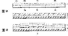
以下参照图2A~图2D,详细说明利用这种压模来制造具有图1的结构的磁记录介质时可能产生的问题。为了明确问题,在图2A~2D中示出了压模20中的凸部的面积比率互相有很大不同的相邻的2个区域。The following will describe in detail the problems that may arise when using such a stamper to manufacture the magnetic recording medium having the structure of FIG. 1 with reference to FIGS. 2A to 2D . In order to clarify the problem, FIGS. 2A to 2D show two adjacent regions in which the area ratios of the protrusions in the
图2A表示在基片31上制作的磁性膜32上涂敷抗蚀剂33,与抗蚀剂33相向地布置了压模20的状态。在该压模20上,凸部的面积比率在左侧区域中减小,在右侧区域中增大。FIG. 2A shows a state where a resist 33 is coated on a
图2B表示施加压力把压模20按压到抗蚀剂33上的压印工序的初期阶段。压模20的凸部被压入到抗蚀剂33中,被凸部挤压出来的抗蚀剂进入到压模20的凹部中。在如图2B的右侧那样凸部的面积比率大的区域中,在该阶段压模20的凹部被挤压出来的抗蚀剂填埋。抗蚀剂的粘度大,在压印时不能够长距离移动。因此,从该状态开始即使再施加压力,在右侧区域内也不能够把凸部压入到抗蚀剂中,增加压印深度。另一方面,在如图2B的左侧那样的凸部的面积比率小的区域中,被凸部挤压出来的抗蚀剂量较少,压模20的凹部未被挤压出来的抗蚀剂填埋。因此,若从该状态开始再施加压力,则能够在左侧区域内把压模20的凸部压入到抗蚀剂中。FIG. 2B shows an initial stage of an imprint process in which pressure is applied to press the
图2C表示压印工序的最终阶段。如该图所示,在右侧区域中状态与图2B相比没有变化。但在左侧区域中,从图2B的状态进一步把凸部压入到抗蚀剂中,增大了压印深度。其结果是压模20的右侧区域和左侧区域之间的中间区域中产生变形。在该阶段,即使在左侧区域内,也是压模20的凹部被挤压出来的抗蚀剂完全填埋。因此,即使从该状态进一步施加压力,也不能够在任何区域内把凸部压入到抗蚀剂中。这样,在不能够进一步增加压印深度的时间点上结束压印。Figure 2C shows the final stage of the embossing process. As shown in the figure, there is no change in state in the right region compared to FIG. 2B. However, in the left region, the protrusion is pressed further into the resist from the state of FIG. 2B , increasing the imprint depth. As a result, deformation occurs in the middle region between the right and left regions of the
图2D表示在压印结束后将压模20除去的状态。如上所述,由于在压模20的右侧区域和左侧区域内压印深度不同,因此残留在磁性膜32上的抗蚀剂残渣的厚度也是在右侧区域和左侧区域中不同。FIG. 2D shows a state where the
若在该状态下将已转印了凹凸的抗蚀剂33作为掩模进行蚀刻处理、对磁性膜32进行加工,则由于抗蚀剂残渣的不同而使磁性膜32的加工膜厚产生不均匀。也就是说,在图2D的左侧区域中,抗蚀剂残渣的厚度t1薄,所以磁性膜32的蚀刻深度相对较深,与此相反,在图2D的右侧区域中,抗蚀剂残渣的厚度t2较厚,所以磁性膜32的蚀刻深度相对较浅。In this state, if the resist 33 on which the unevenness has been transferred is used as a mask to etch the
若更具体地表示数值,则例如以上所述,在利用压印光刻法来制造具有图1A的标记型色同步信号结构的磁记录介质的情况下,采用的压模20如图3A所示,凸部的面积比率在前同步信号部20a中约为50%、在色同步信号部20b中约为75%、在数据部20c中约为33%。而且,为了简化起见,图中未示出压模20中的凸部的图形。另外,地址区的占有面积,与前同步信号区、色同步信号区、数据区相比较小,地址区中的压印深度达到接近于周围的前同步信号区或色同步信号区的压印深度的水平,所以地址区在图中并未示出。If the numerical value is expressed more specifically, then, for example, as described above, in the case of utilizing the imprint lithography method to manufacture a magnetic recording medium having the mark-type burst signal structure of FIG. 1A, the
在这种情况下,前同步信号部20a、色同步信号部20b和数据部20c中的压模20的凸部朝向抗蚀剂33的压印深度如图3B所示。也就是说,压印深度,与凸部的面积比率相对应,在数据部20c中最深,在色同步信号部20b中最浅,在前同步信号部20a中处于两者的中间水平。其结果是,抗蚀剂残渣的厚度,在数据区中最薄,在色同步信号区中最厚,在前同步信号区中处于两者的中间水平。In this case, the embossing depth of the convex portion of the
在该状态下,若用已转印了凹凸的抗蚀剂33作为掩模进行蚀刻处理,则磁性膜32的蚀刻深度,在数据区中最深,在色同步信号区中最浅,在前同步信号区中处于两者的中间水平。所以,蚀刻后的磁性膜32的厚度,在数据区中最薄,在色同步信号区中最厚,在前同步信号区中处于两者的中间水平。这样,在磁性膜32的厚度存在误差的磁记录介质中,对应于磁性膜32的厚度,信号强度和记录特性不同,所以,很难使读写稳定。在具有孔型色同步信号结构的磁记录介质中也产生同样的问题。In this state, if the etching process is performed using the resist 33 on which the unevenness has been transferred as a mask, the etching depth of the
与此相比,在根据本发明实施方式的磁记录介质中,在色同步信号区的非信号部中形成磁性膜的标记。最好是,通过这样在色同步信号区的非信号部中形成磁性膜的标记,在伺服区(前同步信号区和色同步信号区)与数据区之间尽量减小磁性标记的面积比率的差。例如,最好是使色同步信号区中的磁性标记的面积比率,为前同步信号区和数据区中的面积比率的中间值。In contrast, in the magnetic recording medium according to the embodiment of the present invention, the mark of the magnetic film is formed in the non-signal portion of the burst region. Preferably, by forming the mark of the magnetic film in the non-signal portion of the burst signal area in this way, the area ratio of the magnetic mark is reduced as much as possible between the servo area (preamble signal area and color burst signal area) and the data area. Difference. For example, it is preferable to set the area ratio of the magnetic marks in the burst area to be an intermediate value between the area ratios in the preamble area and the data area.
[第1实施方式][the first embodiment]
图4是根据本实施方式的磁记录介质的平面图。如图4所示,该磁记录介质具有:形成了磁性膜的标记的伺服区1,和形成了磁性膜的分离磁道的数据区2。伺服区1包括:前同步信号区11、地址区12、色同步信号区13。FIG. 4 is a plan view of a magnetic recording medium according to the present embodiment. As shown in FIG. 4, the magnetic recording medium has a servo area 1 in which marks of a magnetic film are formed, and a
在前同步信号区11中,线状磁性标记以及其间的非磁性膜沿磁道方向按等间隔形成,所以,磁性标记的面积比率约为50%。在地址区12中,图形因地址值不同而不同,所以磁性标记的面积比率随地址不同而有所不同。数据区2中的磁性分离磁道的面积比率被设定为约67%。这些区与图1中的对应的区相同。In the
图4的色同步信号区13包括信号部13a和非信号部13c,信号部13a和非信号部13c的磁道方向的长度相同。在信号部13a中,磁性膜的4个矩形标记(4个第一标记)以及其间的非磁性膜沿磁道方向按等间隔形成。在信号部13a中包括距离磁道中心的相对位置互不相同的色同步信号A~色同步信号D。该信号部13a也与图1的信号部相同。另一方面,在非信号部13c中,平面几何形状为矩形的磁性膜的11个矩形标记(11个第二标记)以及其间的由非磁性膜填充的空间沿磁道方向按等间隔形成。非信号部13c中的矩形磁性标记的间距与信号部13a中的矩形磁性标记的间距不同。由于在该色同步信号区13中,无论是在信号部13a中还是在非信号部13c中矩形磁性标记以及其间的非磁性空间均沿磁道方向按等间隔形成,因此磁性标记的面积比率约为50%。The
这样,在图4所示的磁记录介质中,磁性标记的面积比率在前同步信号区11中约为50%、在色同步信号区13中约为50%、在数据区2中约为67%,面积比率之差比较小。在上述磁记录介质的制造中所使用的压模中,凸部的面积比率在前同步信号部中约为50%、在色同步信号部中约为50%、在数据部中约为33%。该压模在部位间的凸部的面积比率的差较小,所以,能够抑制压印后的抗蚀剂残渣的厚度的差,通过以该抗蚀剂作为掩模对磁性膜进行蚀刻,能够形成大致上均匀厚度的磁性标记。本实施方式中的色同步信号区包括的磁性标记,无论在信号部13a中还是非信号部13c中均是周期性地形成的,因此没有标记型和孔型的区别。Thus, in the magnetic recording medium shown in FIG. 4, the area ratio of the magnetic marks is about 50% in the
利用根据本实施方式的磁记录介质和具有通常的磁头的磁记录装置,能够进行读写。下面说明从图4所示的磁记录介质中获得的色同步信号。如上所述,在色同步信号区13的信号部13a中并列有4个矩形磁性标记,在非信号部13c中并列有11个矩形磁性标记,在2个区中矩形标记的间距不同。在这种情况下,从信号部13a中获得的信号的频率为4x(x为常数)Hz,从非信号部13c中获得的信号频率为11xHz。因此,将来自非信号部13c的频率成分的信号除去,即可取出来自信号部13a的频率成分的信号。Reading and writing can be performed using the magnetic recording medium according to this embodiment and a magnetic recording device having a normal magnetic head. The burst signal obtained from the magnetic recording medium shown in Fig. 4 will be described below. As described above, four rectangular magnetic marks are juxtaposed in the
再者,如上所述,由于在根据本发明的实施方式的磁记录介质中,形成了大致上均匀厚度的磁性标记,因此能够进行稳定的读写。Furthermore, as described above, in the magnetic recording medium according to the embodiment of the present invention, since magnetic marks having a substantially uniform thickness are formed, stable reading and writing can be performed.
[第2实施方式][the second embodiment]
图5是根据本实施方式的磁记录介质的色同步信号区的平面图。在图5的色同步信号区13中,在非信号部13c中形成了平面形状为在磁道方向上平行的多个长条的磁性膜的线状标记(第二标记)。此外的结构与图4相同。而且,图5的非信号部13c中的线状标记的磁道宽度方向的间距并未特别限定。在这种情况下,线状磁性标记的宽度和线状标记之间的非磁性空间的宽度之比被设定为3∶1,所以,非信号部13c中的磁性标记的面积比率约为75%。相应地,色同步信号区13中的磁性标记的面积比率约为63%。FIG. 5 is a plan view of a burst area of the magnetic recording medium according to the present embodiment. In the
在图5所示的磁记录介质中,磁性标记的面积比率,在前同步信号区11中约为63%,在色同步信号区13中约为50%,在数据区2中约为67%,面积比率的差较小。所以,在该实施方式中也能够获得与第1实施方式相同的效果。In the magnetic recording medium shown in FIG. 5, the area ratio of the magnetic marks is about 63% in the
[第3实施方式][the third embodiment]
图6是根据本实施方式的磁记录介质的色同步信号区的平面图。在图6的色同步信号区13中,在非信号部13c中形成了平面形状为周期性地配制的多个点的磁性膜的点标记。非信号部13c中的点磁性标记(第二标记)的间距与信号部13a中的矩形磁性标记(第一标记)的间距不同。此外的结构与图4相同。而且,图6的非信号部13c中的点标记的磁道宽度方向的间距并未特别限定。在这种情况下,点磁性标记的宽度和标记之间的非磁性空间的宽度之比,在磁道方向上被设定为3∶1,在磁道宽度方向上被设定为3∶1,所以,非信号部13c中的磁性标记的面积比率约为56%。相应地,色同步信号区13中的磁性标记的面积比率约为54%。FIG. 6 is a plan view of a burst region of the magnetic recording medium according to the present embodiment. In the
在图6所示的磁记录介质中,磁性标记的面积比率,在前同步信号区11中约为50%,在色同步信号区13中约为54%,在数据区2中约为67%,面积比率的差较小。并且,由于非信号部13c中的点磁性标记的间距与信号部13a中的矩形磁性标记的间距不同,因此将来自非信号部13c的频率成分的信号除去,即能够取出来自信号部13a的频率成分的信号。相应地,在该实施方式中也能够获得与第1实施方式相同的效果。In the magnetic recording medium shown in FIG. 6, the area ratio of the magnetic marks is about 50% in the
而且,在图4~图6中,通过对色同步信号区13的非信号部13c中的磁性标记的宽度和标记间的非磁性空间的宽度进行适当设定,即可对色同步信号区13整体的磁性标记的面积比率进行调整。4 to 6, by properly setting the width of the magnetic mark in the
并且,色同步信号区13的非信号部13c的结构并非仅限于图4~图6所示的内容。Furthermore, the structure of the
以下参考图7A~图7G,详细说明根据本发明实施方式的磁记录介质的制造方法。A method for manufacturing a magnetic recording medium according to an embodiment of the present invention will be described in detail below with reference to FIGS. 7A to 7G .
首先,如下所述,制造压模。如图7A所示,在原盘21上涂敷电子束抗蚀剂22。最好是,对原盘21采用硅或玻璃。如图7B所示,用电子束直接在电子束抗蚀剂22上扫描后,进行显影,在电子束抗蚀剂22上形成凹凸图形。如图7C所示,对已形成了电子束抗蚀剂22的凹凸图形的原盘21进行电铸处理,将通过电铸而形成的金属盘剥离下来,制成压模20。压模的材料最好是Ni,但并不局限于此。First, a stamper is fabricated as described below. As shown in FIG. 7A, an electron beam resist 22 is applied on the
在压模20的表面上,形成凸部图形,该凸部图形形成例如与图4所示的磁记录介质的磁性标记相反的图形。在这种情况下,压模20上的凸部图形的面积比率,在前同步信号区中约为50%,在色同步信号区中约为50%,在数据区中约为33%。On the surface of the
而且,也可以在图7B之后,将所形成的抗蚀剂图形作为掩模对原盘21进行蚀刻,通过将抗蚀剂的凹凸图形转印到原盘21上,制作出压模。Furthermore, after FIG. 7B , the
随后,如下所述,利用压印光刻法来制作磁记录介质。如图7D所示,在基片31上制作由适用于垂直记录的材料构成的磁性膜32。在这种情况下,最好是形成软磁性基底膜和强磁性记录膜作为磁性膜32,制成垂直二层膜介质。在该磁性膜32上涂敷压印用抗蚀剂33。如图7E所示,使压模20与基片31上的抗蚀剂33相对地施加压力,将压模20按压到抗蚀剂33上,将压模20的表面的凸部图形转印到抗蚀剂33的表面上。然后,取下压模20。如图7F所示,通过将形成了凹凸图形的抗蚀剂33作为掩模对磁性膜32进行蚀刻,来对磁性膜32进行加工。其结果是,形成如图4所示的磁性标记的图形。这时,磁性标记的面积比率,在前同步信号区中约为50%,在色同步信号区中约为50%,在数据区中约为67%。如图7G所示,通过在磁性膜32上设置碳保护膜34,再涂敷润滑剂,制成磁记录介质。Subsequently, as described below, a magnetic recording medium was fabricated using imprint lithography. As shown in FIG. 7D, a
在采用如上述的压模20那样部位间的凸部图形的面积比率的差较小的压模的情况下,能够抑制压印后抗蚀剂残渣的厚度的差,通过将该抗蚀剂作为掩模对磁性膜进行蚀刻,能够形成大致上均匀厚度的磁性标记。In the case of using a stamper with a small difference in the area ratio of the convex portion pattern between parts like the
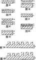
图8A中表示具有图4所示的磁性标记的图形的磁性膜的断面,图8B中表示具有图1A所示的磁性标记的图形的磁性膜的断面。在图8A的情况下(本发明),压模的部位间的凸部图形的面积比率的差较小,无论在介质上的什么位置上都能够使压印后的抗蚀剂的残渣的膜厚大致上均匀,因此,加工后的磁性标记32的膜厚也大致均匀。另一方面,在图8B的情况下(比较例),压模的部位间的凸部图形的面积比率的差较大,由于随着介质上的位置不同压印后的抗蚀剂残渣的膜厚变得不均匀,因此加工后的磁性标记32的膜厚也不均匀。若使用图8B的介质,则会出现磁头振动和记录失败等问题,但在图8A的介质中则不会出现这样的问题。FIG. 8A shows a cross section of a magnetic film having the pattern of magnetic marks shown in FIG. 4, and FIG. 8B shows a cross section of a magnetic film having the pattern of magnetic marks shown in FIG. 1A. In the case of FIG. 8A (the present invention), the difference in the area ratio of the convex portion pattern between the parts of the stamper is small, and the film of the resist residue after imprinting can be formed no matter where on the medium. Since the thickness is substantially uniform, the film thickness of the processed
以下说明根据本发明另一实施方式的基片加工型磁记录介质(Substrate-patterned Discrete track media)。在基片加工型磁记录介质中,也能够获得与参照图7说明的磁性膜加工型磁记录介质(magnetic film-patterned Discrete track media)相同的效果。在基片加工型磁记录装置中,凸部磁性膜和凹部磁性膜分别对应于磁性膜加工型磁记录介质的磁性标记和非磁性膜。参照图9A~图9G,说明基片加工型磁记录介质的制造方法。A substrate-patterned magnetic recording medium (Substrate-patterned Discrete track media) according to another embodiment of the present invention will be described below. Also in the substrate processed magnetic recording medium, the same effect as that of the magnetic film-patterned discrete track media described with reference to FIG. 7 can be obtained. In the substrate processing type magnetic recording device, the convex portion magnetic film and the concave portion magnetic film correspond to the magnetic marks and the nonmagnetic film of the magnetic film processing type magnetic recording medium, respectively. Referring to FIGS. 9A to 9G , a method of manufacturing a substrate processing type magnetic recording medium will be described.
图9A至图9C所示的压模的制造方法与图7A~图7C所示的方法相同。The manufacturing method of the stamper shown in FIGS. 9A to 9C is the same as the method shown in FIGS. 7A to 7C .
其次,如下所述,利用压印光刻法来制作在表面上加工凹凸的基片。如图9D所示,在基片41上涂敷压印用的抗蚀剂42。如图9E所示,使压模20与基片41上的抗蚀剂42相对地施加压力,将压模20按压到抗蚀剂42上,将压模20表面的凸部图形转印到抗蚀剂42表面。然后,取下压模20。如图9F所示,通过以形成了凹凸图形的抗蚀剂42作为掩模对基片41进行蚀刻,来对基片41进行加工。其结果是,与图4A所示的磁性标记相对应的凸部的图形形成在基片41的表面上。这时,凸部的面积比率,在前同步信号区中约为50%,在色同步信号区中约为50%,在数据区中约为67%。如图9G所示,在基片41的凸部上和凹部内制作由适用于垂直记录的材料构成的磁性膜43。在这种情况下,最好是形成软磁性基底膜和强磁性记录膜作为磁性膜43,制成垂直二层膜介质。通过在磁性膜43上设置碳保护膜44,再涂敷润滑剂,制成磁记录介质。Next, as described below, a substrate with unevenness processed on the surface was produced by imprint lithography. As shown in FIG. 9D , a resist 42 for imprinting is applied on a
在采用如上述的压模20那样的部位间的凸部图形的面积比率的差较小的压模的情况下,能够抑制压印后抗蚀剂残渣的厚度差,通过用该抗蚀剂作为掩模对基片进行蚀刻,能够形成大致上均匀的高度的凸部图形。In the case of using a stamper such as the
图10A中表示与图4相对应的基片加工型分离磁道介质的基片的断面,图10B中表示与图1A相对应的基片加工型分离磁道介质的基片的断面。在图10A的情况下(本发明),由于压模的部位间的凸部图形的面积比率的差较小,无论在基片上的什么位置上都能够使压印后的抗蚀剂的残渣的膜厚大致上均匀,因此加工后的基片表面的凸部的高度也大致均匀。另一方面,在图10B的情况下(比较例),压模的部位间的凸部图形的面积比率的差较大,由于随着基片上的位置不同压印后的抗蚀剂残渣的膜厚变得不均匀,因此加工后的基片表面的凸部的高度也不均匀。若使用由图10B的基片制成的介质,则会出现磁头振动和记录失败等问题,但在利用图10A的基片而制作的介质中则不会出现这样的问题。FIG. 10A shows a cross section of the substrate of the substrate processing type split track medium corresponding to FIG. 4, and FIG. 10B shows a cross section of the substrate of the substrate processing type split track medium corresponding to FIG. 1A. In the case of FIG. 10A (the present invention), since the difference in the area ratio of the convex pattern between the parts of the stamper is small, the residue of the resist after imprinting can be reduced no matter where on the substrate. Since the film thickness is substantially uniform, the height of the protrusions on the processed substrate surface is also substantially uniform. On the other hand, in the case of FIG. 10B (comparative example), the difference in the area ratio of the convex portion pattern between the parts of the stamper is large, and the film of resist residue after imprinting varies with the position on the substrate. Since the thickness becomes non-uniform, the height of the protrusions on the processed substrate surface is also non-uniform. If a medium made of the substrate of FIG. 10B is used, problems such as head vibration and recording failure occur, but such problems do not occur in a medium made of the substrate of FIG. 10A.
以下参照图11,说明根据本发明实施方式的磁记录装置。磁记录装置150是采用旋转式传动装置的方式的装置。在该图中,具有如图4~图6所示的磁性标记的图形的磁盘30,被安装在主轴152上,响应于来自图中未示出的驱动装置控制部的控制信号,通过图中未示出的马达,沿箭头A方向旋转。磁记录装置150也可以具有多个磁盘30。A magnetic recording device according to an embodiment of the present invention will be described below with reference to FIG. 11 . The
对磁盘30内存储的信息进行读写的磁头滑动器153安装在薄片状的悬架154的前端上。悬架154与传动装置臂155的一端相连接。在传动装置臂155的另一端上设置了作为线性马达的一种的音圈马达156。音圈马达156具有:卷绕在线轴部上的图中未示出的驱动线圈,和由夹持上述线圈而相对设置的永久磁铁和对置轭铁所构成的磁回路。传动装置臂155通过设置在枢轴157的上下2处的图中未示出的滚珠轴承而被支承,并因音圈马达156而可以自由旋转。A
若磁盘3旋转,则磁头滑动器153的面向介质的面(ABS)被保持为,距离磁盘30的表面具有预定的上浮量。而且,也可以是滑动器与磁盘30接触的所谓“接触行走式”。When the magnetic disk 3 rotates, the medium-facing surface (ABS) of the
在根据本发明实施方式的磁记录装置中,由于磁盘30的磁性膜形成大致上均匀的膜厚,因此能够进行稳定的读写。In the magnetic recording device according to the embodiment of the present invention, since the magnetic film of the
附加的优点和变型对于本领域的技术人员来说是很容易想到的。因此,本发明在更广泛的方面来说并非局限于此处所显示和说明的具体细节和代表性实施例。相应地,在不脱离随附的权利要求书及其等同物所限定的本发明总的概念的精神和范围的情况下,可以做出各种变型。Additional advantages and modifications will readily occur to those skilled in the art. Therefore, the invention in its broader aspects is not limited to the specific details and representative embodiments shown and described herein. Accordingly, various modifications may be made without departing from the spirit and scope of the general inventive concept as defined by the appended claims and their equivalents.
Claims (17)
Applications Claiming Priority (2)
| Application Number | Priority Date | Filing Date | Title |
|---|---|---|---|
| JP108107/2004 | 2004-03-31 | ||
| JP2004108107AJP4074262B2 (en) | 2004-03-31 | 2004-03-31 | Magnetic recording medium, manufacturing method thereof, and magnetic recording / reproducing apparatus |
Publications (2)
| Publication Number | Publication Date |
|---|---|
| CN1677494A CN1677494A (en) | 2005-10-05 |
| CN100377210Ctrue CN100377210C (en) | 2008-03-26 |
Family
ID=34940619
Family Applications (1)
| Application Number | Title | Priority Date | Filing Date |
|---|---|---|---|
| CNB2005100600872AExpired - Fee RelatedCN100377210C (en) | 2004-03-31 | 2005-03-31 | Magnetic recording medium, manufacturing method thereof, and magnetic recording device |
Country Status (4)
| Country | Link |
|---|---|
| US (1) | US7388725B2 (en) |
| EP (1) | EP1596398A3 (en) |
| JP (1) | JP4074262B2 (en) |
| CN (1) | CN100377210C (en) |
Families Citing this family (41)
| Publication number | Priority date | Publication date | Assignee | Title |
|---|---|---|---|---|
| JP4358067B2 (en)* | 2004-08-06 | 2009-11-04 | 株式会社東芝 | Magnetic recording medium and magnetic recording apparatus |
| JP4077437B2 (en)* | 2004-09-16 | 2008-04-16 | Tdk株式会社 | Information recording medium and recording / reproducing apparatus |
| JP2006216171A (en)* | 2005-02-04 | 2006-08-17 | Tdk Corp | Magnetic recording medium, recording or reproducing apparatus, and stamper |
| US7548388B2 (en)* | 2005-02-16 | 2009-06-16 | Tdk Corporation | Magnetic recording medium, recording/reproducing apparatus, and stamper |
| CN100429697C (en)* | 2005-02-16 | 2008-10-29 | Tdk股份有限公司 | Magnetic recording medium, recording/reproducing apparatus, and stamper |
| JP2006228347A (en)* | 2005-02-18 | 2006-08-31 | Sony Corp | Method for manufacturing magnetic disk |
| JP4218896B2 (en) | 2005-03-02 | 2009-02-04 | Tdk株式会社 | Magnetic recording medium, recording / reproducing apparatus, and stamper |
| JP2006260713A (en) | 2005-03-18 | 2006-09-28 | Toshiba Corp | Recording medium, recording / reproducing apparatus, and recording / reproducing method |
| JP4649262B2 (en)* | 2005-04-19 | 2011-03-09 | 株式会社東芝 | Method for manufacturing magnetic recording medium |
| JP4542953B2 (en) | 2005-06-10 | 2010-09-15 | 株式会社東芝 | Magnetic disk medium and magnetic recording / reproducing apparatus |
| JP4581963B2 (en)* | 2005-10-27 | 2010-11-17 | Tdk株式会社 | Stamper, uneven pattern forming method, and information recording medium manufacturing method |
| JP4675758B2 (en) | 2005-11-16 | 2011-04-27 | 昭和電工株式会社 | Magnetic recording medium |
| JP2007164958A (en)* | 2005-11-21 | 2007-06-28 | Tdk Corp | Recording/reproducing apparatus and method of measuring parameter |
| KR100738101B1 (en)* | 2006-01-26 | 2007-07-12 | 삼성전자주식회사 | Patterned Media and Manufacturing Method Thereof |
| JP4533854B2 (en) | 2006-03-06 | 2010-09-01 | 株式会社東芝 | Magnetic recording / reproducing apparatus, magnetic recording method, and magnetic recording / reproducing method |
| JP4585476B2 (en) | 2006-03-16 | 2010-11-24 | 株式会社東芝 | Patterned medium and magnetic recording apparatus |
| JP2007287300A (en) | 2006-03-24 | 2007-11-01 | Fujitsu Ltd | Magnetic recording medium manufacturing method and magnetic recording medium |
| JP4675812B2 (en)* | 2006-03-30 | 2011-04-27 | 株式会社東芝 | Magnetic recording medium, magnetic recording apparatus, and method of manufacturing magnetic recording medium |
| JP4551880B2 (en)* | 2006-03-30 | 2010-09-29 | 株式会社東芝 | Method for manufacturing magnetic recording medium |
| JP2007273042A (en)* | 2006-03-31 | 2007-10-18 | Toshiba Corp | Magnetic recording medium and magnetic recording / reproducing apparatus |
| JP4543004B2 (en)* | 2006-05-11 | 2010-09-15 | 株式会社東芝 | Pattern forming method, imprint mold, and magnetic recording medium manufacturing method |
| JP4728892B2 (en)* | 2006-06-30 | 2011-07-20 | 株式会社東芝 | Magnetic recording medium and method for manufacturing the same |
| JP2008016084A (en)* | 2006-07-03 | 2008-01-24 | Toshiba Corp | Method for manufacturing magnetic recording medium |
| JP2008084395A (en)* | 2006-09-26 | 2008-04-10 | Fujitsu Ltd | Patterned media clock extraction method and circuit |
| WO2008053547A1 (en)* | 2006-11-01 | 2008-05-08 | Fujitsu Limited | Pattern transferring stamper, method for manufacturing magnetic recording medium using the pattern transferring stamper, and the magnetic recording medium |
| US20080190483A1 (en)* | 2007-02-13 | 2008-08-14 | Carpenter R Douglas | Composition and method of preparing nanoscale thin film photovoltaic materials |
| JP2008226395A (en)* | 2007-03-15 | 2008-09-25 | Fujitsu Ltd | Magnetic disk, stamper used for manufacturing the magnetic disk, and method for manufacturing the magnetic disk |
| JP2008243266A (en)* | 2007-03-26 | 2008-10-09 | Hitachi Global Storage Technologies Netherlands Bv | Magnetic recording medium, servo recording method on magnetic recording medium, and magnetic recording apparatus |
| JP2008282512A (en)* | 2007-05-14 | 2008-11-20 | Toshiba Corp | Magnetic recording medium and magnetic recording / reproducing apparatus |
| JP2009006619A (en)* | 2007-06-29 | 2009-01-15 | Hitachi Ltd | Nanoimprint mold and recording medium |
| KR100900201B1 (en)* | 2007-07-04 | 2009-06-02 | 삼성전자주식회사 | Method of measuring JR offset of magnetic recording medium, hard disk drive and hard disk drive |
| JP2007287322A (en)* | 2007-07-09 | 2007-11-01 | Tdk Corp | Information recording medium and recording/reproducing device |
| KR100924698B1 (en)* | 2007-07-24 | 2009-11-03 | 삼성전자주식회사 | Magnetic recording device |
| JP4908339B2 (en)* | 2007-07-30 | 2012-04-04 | 株式会社東芝 | Disk storage device and disk medium |
| JP5004225B2 (en)* | 2007-09-19 | 2012-08-22 | 独立行政法人産業技術総合研究所 | Mold manufacturing method for imprint lithography |
| JP4382843B2 (en) | 2007-09-26 | 2009-12-16 | 株式会社東芝 | Magnetic recording medium and method for manufacturing the same |
| KR20090059848A (en)* | 2007-12-07 | 2009-06-11 | 삼성전자주식회사 | Method for recording track information on a pattern magnetic recording medium and a pattern magnetic recording medium |
| JP2010009729A (en)* | 2008-06-30 | 2010-01-14 | Toshiba Corp | Imprint stamper, method of manufacturing imprint stamper, magnetic recording medium, method of manufacturing magnetic recording medium and magnetic disk apparatus |
| JP2008310957A (en)* | 2008-09-29 | 2008-12-25 | Tdk Corp | Magnetic recording medium, recording and reproducing device, and stamper |
| JP5050105B2 (en)* | 2011-01-12 | 2012-10-17 | 株式会社東芝 | Magnetic recording device |
| US20220253619A1 (en)* | 2021-02-08 | 2022-08-11 | Mark Eklund | Micro-track device (M-TDnm) |
Citations (4)
| Publication number | Priority date | Publication date | Assignee | Title |
|---|---|---|---|---|
| JPH0765363A (en)* | 1993-08-26 | 1995-03-10 | Hitachi Ltd | Magnetic recording medium, magnetic recording apparatus, and manufacturing method thereof |
| JP2000306227A (en)* | 1999-02-19 | 2000-11-02 | Tdk Corp | Magnetic recording medium |
| US6643082B1 (en)* | 1999-06-08 | 2003-11-04 | Seagate Technology Llc | Servo sector format for a patterned media |
| CN1542750A (en)* | 2003-03-26 | 2004-11-03 | TDK�ɷ�����˾ | Magnetic recording medium and method of manufacturing magnetic recording medium |
Family Cites Families (6)
| Publication number | Priority date | Publication date | Assignee | Title |
|---|---|---|---|---|
| JPS62256225A (en)* | 1986-04-30 | 1987-11-07 | Hitachi Ltd | magnetic disk |
| JPH02301018A (en)* | 1989-05-16 | 1990-12-13 | Sony Corp | Magnetic recording medium |
| JP2946636B2 (en)* | 1990-05-21 | 1999-09-06 | ソニー株式会社 | Track address pattern of magnetic disk drive |
| JP2000067538A (en)* | 1998-08-24 | 2000-03-03 | Alps Electric Co Ltd | Disk on which servo patterns are recorded and arithmetic processing method for patterns read from the same |
| JP3757098B2 (en)* | 2000-06-01 | 2006-03-22 | 富士通株式会社 | Disk device and disk medium |
| AU2001290870A1 (en)* | 2000-09-12 | 2002-03-26 | Seagate Technology Llc | Method and apparatus for minimizing slider fly heights over patterned media |
- 2004
- 2004-03-31JPJP2004108107Apatent/JP4074262B2/ennot_activeExpired - Fee Related
- 2005
- 2005-03-22EPEP05251760Apatent/EP1596398A3/ennot_activeWithdrawn
- 2005-03-24USUS11/087,595patent/US7388725B2/ennot_activeExpired - Fee Related
- 2005-03-31CNCNB2005100600872Apatent/CN100377210C/ennot_activeExpired - Fee Related
Patent Citations (4)
| Publication number | Priority date | Publication date | Assignee | Title |
|---|---|---|---|---|
| JPH0765363A (en)* | 1993-08-26 | 1995-03-10 | Hitachi Ltd | Magnetic recording medium, magnetic recording apparatus, and manufacturing method thereof |
| JP2000306227A (en)* | 1999-02-19 | 2000-11-02 | Tdk Corp | Magnetic recording medium |
| US6643082B1 (en)* | 1999-06-08 | 2003-11-04 | Seagate Technology Llc | Servo sector format for a patterned media |
| CN1542750A (en)* | 2003-03-26 | 2004-11-03 | TDK�ɷ�����˾ | Magnetic recording medium and method of manufacturing magnetic recording medium |
Also Published As
| Publication number | Publication date |
|---|---|
| CN1677494A (en) | 2005-10-05 |
| EP1596398A2 (en) | 2005-11-16 |
| JP4074262B2 (en) | 2008-04-09 |
| JP2005293730A (en) | 2005-10-20 |
| EP1596398A3 (en) | 2006-11-22 |
| US7388725B2 (en) | 2008-06-17 |
| US20050219730A1 (en) | 2005-10-06 |
Similar Documents
| Publication | Publication Date | Title |
|---|---|---|
| CN100377210C (en) | Magnetic recording medium, manufacturing method thereof, and magnetic recording device | |
| JP4724060B2 (en) | Magnetic disk unit | |
| US7505220B2 (en) | Magnetic recording medium, recording/reproducing apparatus, and stamper | |
| US7850441B2 (en) | Mold structure | |
| KR20010088331A (en) | Master carrier for magnetic transfer | |
| CN100538828C (en) | Magnetic recording medium, recording/displaying device and pressing mold | |
| US7105280B1 (en) | Utilizing permanent master for making stampers/imprinters for patterning of recording media | |
| US20080226946A1 (en) | Magnetic disc, stamper for making magnetic disc, and method for making magnetic disc | |
| US7754354B2 (en) | Patterned medium and method of manufacturing the same | |
| JP2006338738A (en) | Magnetic recording medium, magnetic recording and reproducing apparatus, stamper, manufacturing method of stamper, and manufacturing method of magnetic recording medium | |
| JP4110204B2 (en) | Magnetic recording medium, manufacturing method thereof, and magnetic recording / reproducing apparatus | |
| US8085648B2 (en) | Servo master magnetically transferring servo patterns to magnetic recording medium, and magnetic transfer method using the servo master | |
| US7105238B2 (en) | Master information carrier for magnetic transfer | |
| US7522362B2 (en) | Amplitude servo pattern, magnetic recording medium and the manufacturing method, patterned magnetic transfer master substrate used in the manufacturing method, and magnetic recording/reproducing apparatus | |
| JP2007335001A (en) | Magnetic transfer method, magnetic transfer apparatus, magnetic recording medium, magnetic recording / reproducing apparatus | |
| JP3898704B2 (en) | Magnetic recording medium, manufacturing method thereof, and imprint stamper | |
| KR20030007107A (en) | Master carrier for magnetic transfer | |
| JP2001307324A (en) | Magnetic transferring master carrier and magnetic recording medium | |
| KR101440130B1 (en) | Master recording medium with improved magnetic transfer performance | |
| JP2020035506A (en) | Master for transferring magnetic pattern and manufacturing method thereof, and magnetic pattern transferring method | |
| KR20010082119A (en) | Master carrier for magnetic transfer and magnetic recording medium | |
| US20050277000A1 (en) | Process for producing magnetic recording medium with limited coercivity squareness ratio | |
| JP2004079059A (en) | Master carrier for magnetic transfer |
Legal Events
| Date | Code | Title | Description |
|---|---|---|---|
| C06 | Publication | ||
| PB01 | Publication | ||
| C10 | Entry into substantive examination | ||
| SE01 | Entry into force of request for substantive examination | ||
| C14 | Grant of patent or utility model | ||
| GR01 | Patent grant | ||
| CF01 | Termination of patent right due to non-payment of annual fee | Granted publication date:20080326 Termination date:20150331 | |
| EXPY | Termination of patent right or utility model |