CN100367528C - Switching device with memory effect - Google Patents
Switching device with memory effectDownload PDFInfo
- Publication number
- CN100367528C CN100367528CCNB028117433ACN02811743ACN100367528CCN 100367528 CCN100367528 CCN 100367528CCN B028117433 ACNB028117433 ACN B028117433ACN 02811743 ACN02811743 ACN 02811743ACN 100367528 CCN100367528 CCN 100367528C
- Authority
- CN
- China
- Prior art keywords
- state
- switching device
- switch
- active region
- electric field
- Prior art date
- Legal status (The legal status is an assumption and is not a legal conclusion. Google has not performed a legal analysis and makes no representation as to the accuracy of the status listed.)
- Expired - Fee Related
Links
- 230000003446memory effectEffects0.000title1
- 230000005684electric fieldEffects0.000claimsabstractdescription35
- 239000000758substrateSubstances0.000claimsdescription16
- 150000002500ionsChemical class0.000claimsdescription15
- VEXZGXHMUGYJMC-UHFFFAOYSA-MChloride anionChemical compound[Cl-]VEXZGXHMUGYJMC-UHFFFAOYSA-M0.000claimsdescription12
- 150000001875compoundsChemical class0.000claimsdescription10
- 229910001415sodium ionInorganic materials0.000claimsdescription9
- 239000011159matrix materialSubstances0.000claimsdescription7
- 238000000034methodMethods0.000claimsdescription7
- 230000000694effectsEffects0.000claimsdescription5
- 238000013500data storageMethods0.000claimsdescription4
- 229920000642polymerPolymers0.000claimsdescription4
- 125000003118aryl groupChemical group0.000claimsdescription3
- 125000000623heterocyclic groupChemical group0.000claimsdescription3
- 150000004032porphyrinsChemical class0.000claimsdescription3
- 239000000126substanceSubstances0.000claimsdescription3
- 230000004888barrier functionEffects0.000claims5
- FKNQFGJONOIPTF-UHFFFAOYSA-NSodium cationChemical compound[Na+]FKNQFGJONOIPTF-UHFFFAOYSA-N0.000claims2
- 238000009342intercroppingMethods0.000claims2
- NCMHKCKGHRPLCM-UHFFFAOYSA-Ncaesium(1+)Chemical compound[Cs+]NCMHKCKGHRPLCM-UHFFFAOYSA-N0.000claims1
- IEQIEDJGQAUEQZ-UHFFFAOYSA-NphthalocyanineChemical compoundN1C(N=C2C3=CC=CC=C3C(N=C3C4=CC=CC=C4C(=N4)N3)=N2)=C(C=CC=C2)C2=C1N=C1C2=CC=CC=C2C4=N1IEQIEDJGQAUEQZ-UHFFFAOYSA-N0.000claims1
- FAPWRFPIFSIZLT-UHFFFAOYSA-MSodium chlorideChemical compound[Na+].[Cl-]FAPWRFPIFSIZLT-UHFFFAOYSA-M0.000description8
- 230000009471actionEffects0.000description6
- 239000000203mixtureSubstances0.000description6
- 210000004027cellAnatomy0.000description5
- 239000002131composite materialSubstances0.000description5
- -1polyethylenePolymers0.000description5
- 238000010586diagramMethods0.000description4
- 239000011780sodium chlorideSubstances0.000description4
- 229920000547conjugated polymerPolymers0.000description3
- 230000006870functionEffects0.000description3
- 230000007246mechanismEffects0.000description3
- 238000012545processingMethods0.000description3
- AIYUHDOJVYHVIT-UHFFFAOYSA-Mcaesium chlorideChemical compound[Cl-].[Cs+]AIYUHDOJVYHVIT-UHFFFAOYSA-M0.000description2
- 150000001768cationsChemical class0.000description2
- 230000008859changeEffects0.000description2
- 239000013078crystalSubstances0.000description2
- 230000005611electricityEffects0.000description2
- 238000005516engineering processMethods0.000description2
- 230000005669field effectEffects0.000description2
- 229910010272inorganic materialInorganic materials0.000description2
- 238000009413insulationMethods0.000description2
- 238000005442molecular electronicMethods0.000description2
- 229920001197polyacetylenePolymers0.000description2
- 229910052594sapphireInorganic materials0.000description2
- 239000010980sapphireSubstances0.000description2
- 238000000926separation methodMethods0.000description2
- 159000000000sodium saltsChemical class0.000description2
- 230000003068static effectEffects0.000description2
- 239000010409thin filmSubstances0.000description2
- 238000012546transferMethods0.000description2
- YMWLPMGFZYFLRP-UHFFFAOYSA-N2-(4,5-dimethyl-1,3-diselenol-2-ylidene)-4,5-dimethyl-1,3-diselenoleChemical compound[Se]1C(C)=C(C)[Se]C1=C1[Se]C(C)=C(C)[Se]1YMWLPMGFZYFLRP-UHFFFAOYSA-N0.000description1
- ZAMOUSCENKQFHK-UHFFFAOYSA-NChlorine atomChemical compound[Cl]ZAMOUSCENKQFHK-UHFFFAOYSA-N0.000description1
- DGAQECJNVWCQMB-PUAWFVPOSA-MIlexoside XXIXChemical compoundC[C@@H]1CC[C@@]2(CC[C@@]3(C(=CC[C@H]4[C@]3(CC[C@@H]5[C@@]4(CC[C@@H](C5(C)C)OS(=O)(=O)[O-])C)C)[C@@H]2[C@]1(C)O)C)C(=O)O[C@H]6[C@@H]([C@H]([C@@H]([C@H](O6)CO)O)O)O.[Na+]DGAQECJNVWCQMB-PUAWFVPOSA-M0.000description1
- 229910020050NbSe3Inorganic materials0.000description1
- 239000004698PolyethyleneSubstances0.000description1
- 125000002015acyclic groupChemical group0.000description1
- HSFWRNGVRCDJHI-UHFFFAOYSA-Nalpha-acetyleneNatural productsC#CHSFWRNGVRCDJHI-UHFFFAOYSA-N0.000description1
- 229910052782aluminiumInorganic materials0.000description1
- XAGFODPZIPBFFR-UHFFFAOYSA-NaluminiumChemical compound[Al]XAGFODPZIPBFFR-UHFFFAOYSA-N0.000description1
- 150000001450anionsChemical class0.000description1
- 230000009286beneficial effectEffects0.000description1
- 229910052792caesiumInorganic materials0.000description1
- TVFDJXOCXUVLDH-UHFFFAOYSA-Ncaesium atomChemical compound[Cs]TVFDJXOCXUVLDH-UHFFFAOYSA-N0.000description1
- 239000003990capacitorSubstances0.000description1
- 239000000969carrierSubstances0.000description1
- 239000000460chlorineSubstances0.000description1
- 229910052801chlorineInorganic materials0.000description1
- 230000021615conjugationEffects0.000description1
- 238000011161developmentMethods0.000description1
- 238000006073displacement reactionMethods0.000description1
- 239000011521glassSubstances0.000description1
- 150000002484inorganic compoundsChemical class0.000description1
- 239000011147inorganic materialSubstances0.000description1
- 239000012212insulatorSubstances0.000description1
- 230000003993interactionEffects0.000description1
- 230000014759maintenance of locationEffects0.000description1
- 239000000463materialSubstances0.000description1
- 230000006386memory functionEffects0.000description1
- 230000004048modificationEffects0.000description1
- 238000012986modificationMethods0.000description1
- 239000002120nanofilmSubstances0.000description1
- 230000000704physical effectEffects0.000description1
- 229920000573polyethylenePolymers0.000description1
- 238000005036potential barrierMethods0.000description1
- 230000008569processEffects0.000description1
- 230000005855radiationEffects0.000description1
- 230000004044responseEffects0.000description1
- 150000003839saltsChemical class0.000description1
- 229910052708sodiumInorganic materials0.000description1
- 239000011734sodiumSubstances0.000description1
- 210000000352storage cellAnatomy0.000description1
- 229910052723transition metalInorganic materials0.000description1
Images


Classifications
- G—PHYSICS
- G01—MEASURING; TESTING
- G01N—INVESTIGATING OR ANALYSING MATERIALS BY DETERMINING THEIR CHEMICAL OR PHYSICAL PROPERTIES
- G01N27/00—Investigating or analysing materials by the use of electric, electrochemical, or magnetic means
- G01N27/26—Investigating or analysing materials by the use of electric, electrochemical, or magnetic means by investigating electrochemical variables; by using electrolysis or electrophoresis
- G01N27/403—Cells and electrode assemblies
- G01N27/414—Ion-sensitive or chemical field-effect transistors, i.e. ISFETS or CHEMFETS
- B—PERFORMING OPERATIONS; TRANSPORTING
- B82—NANOTECHNOLOGY
- B82Y—SPECIFIC USES OR APPLICATIONS OF NANOSTRUCTURES; MEASUREMENT OR ANALYSIS OF NANOSTRUCTURES; MANUFACTURE OR TREATMENT OF NANOSTRUCTURES
- B82Y10/00—Nanotechnology for information processing, storage or transmission, e.g. quantum computing or single electron logic
- G—PHYSICS
- G11—INFORMATION STORAGE
- G11C—STATIC STORES
- G11C13/00—Digital stores characterised by the use of storage elements not covered by groups G11C11/00, G11C23/00, or G11C25/00
- G11C13/0002—Digital stores characterised by the use of storage elements not covered by groups G11C11/00, G11C23/00, or G11C25/00 using resistive RAM [RRAM] elements
- G11C13/0009—RRAM elements whose operation depends upon chemical change
- G11C13/0014—RRAM elements whose operation depends upon chemical change comprising cells based on organic memory material
- H—ELECTRICITY
- H10—SEMICONDUCTOR DEVICES; ELECTRIC SOLID-STATE DEVICES NOT OTHERWISE PROVIDED FOR
- H10D—INORGANIC ELECTRIC SEMICONDUCTOR DEVICES
- H10D48/00—Individual devices not covered by groups H10D1/00 - H10D44/00
- H10D48/30—Devices controlled by electric currents or voltages
- H10D48/32—Devices controlled by only the electric current supplied, or only the electric potential applied, to an electrode which does not carry the current to be rectified, amplified or switched
- H10D48/366—Multistable devices; Devices having two or more distinct operating states
- H—ELECTRICITY
- H10—SEMICONDUCTOR DEVICES; ELECTRIC SOLID-STATE DEVICES NOT OTHERWISE PROVIDED FOR
- H10K—ORGANIC ELECTRIC SOLID-STATE DEVICES
- H10K10/00—Organic devices specially adapted for rectifying, amplifying, oscillating or switching; Organic capacitors or resistors having potential barriers
- H10K10/40—Organic transistors
- H10K10/46—Field-effect transistors, e.g. organic thin-film transistors [OTFT]
- H10K10/462—Insulated gate field-effect transistors [IGFETs]
- H10K10/464—Lateral top-gate IGFETs comprising only a single gate
- H—ELECTRICITY
- H10—SEMICONDUCTOR DEVICES; ELECTRIC SOLID-STATE DEVICES NOT OTHERWISE PROVIDED FOR
- H10K—ORGANIC ELECTRIC SOLID-STATE DEVICES
- H10K10/00—Organic devices specially adapted for rectifying, amplifying, oscillating or switching; Organic capacitors or resistors having potential barriers
- H10K10/40—Organic transistors
- H10K10/46—Field-effect transistors, e.g. organic thin-film transistors [OTFT]
- H10K10/462—Insulated gate field-effect transistors [IGFETs]
- H10K10/484—Insulated gate field-effect transistors [IGFETs] characterised by the channel regions
- H—ELECTRICITY
- H10—SEMICONDUCTOR DEVICES; ELECTRIC SOLID-STATE DEVICES NOT OTHERWISE PROVIDED FOR
- H10K—ORGANIC ELECTRIC SOLID-STATE DEVICES
- H10K10/00—Organic devices specially adapted for rectifying, amplifying, oscillating or switching; Organic capacitors or resistors having potential barriers
- H10K10/50—Bistable switching devices
- H—ELECTRICITY
- H10—SEMICONDUCTOR DEVICES; ELECTRIC SOLID-STATE DEVICES NOT OTHERWISE PROVIDED FOR
- H10K—ORGANIC ELECTRIC SOLID-STATE DEVICES
- H10K10/00—Organic devices specially adapted for rectifying, amplifying, oscillating or switching; Organic capacitors or resistors having potential barriers
- H10K10/701—Organic molecular electronic devices
- G—PHYSICS
- G11—INFORMATION STORAGE
- G11C—STATIC STORES
- G11C2213/00—Indexing scheme relating to G11C13/00 for features not covered by this group
- G11C2213/10—Resistive cells; Technology aspects
- G11C2213/13—Dissociation, i.e. using memory material including molecules which, during a write operation, are dissociated in ions which migrate further in the memory material
Landscapes
- Engineering & Computer Science (AREA)
- Chemical & Material Sciences (AREA)
- Physics & Mathematics (AREA)
- Nanotechnology (AREA)
- Mathematical Physics (AREA)
- Theoretical Computer Science (AREA)
- Crystallography & Structural Chemistry (AREA)
- Spectroscopy & Molecular Physics (AREA)
- Health & Medical Sciences (AREA)
- Life Sciences & Earth Sciences (AREA)
- Molecular Biology (AREA)
- Chemical Kinetics & Catalysis (AREA)
- Electrochemistry (AREA)
- Analytical Chemistry (AREA)
- Biochemistry (AREA)
- General Health & Medical Sciences (AREA)
- General Physics & Mathematics (AREA)
- Immunology (AREA)
- Pathology (AREA)
- Microelectronics & Electronic Packaging (AREA)
- Semiconductor Memories (AREA)
- Thin Film Transistor (AREA)
Abstract
Translated fromChinese
Description
Translated fromChinese相关内容related information
有关该主题的技术内容揭露于美国申请专利号为60/289,057,标题为“电性可定址的储存器开关”,申请日为2001年5月7日。Technical content on this subject is disclosed in US Patent Application No. 60/289,057, entitled "Electrically Addressable Memory Switch," filed May 7, 2001.
技术领域technical field
本发明有关于一种开关装置,更具体而言,是一种具有储存功能的开关装置,其中储存/开关装置可被定址,且开关状态可由外部所施加的电场来反转。The present invention relates to a switching device, more particularly, a switching device with memory function, wherein the memory/switching device can be addressed and the switching state can be reversed by an externally applied electric field.
背景技术Background technique
众所周知,各类电性可定址的储存器装置是用于计算机的资料储存。其中,大多数该类装置将数据位作为电荷储存在电容器内。电荷的状态可被读出,且其输出信号输送至计算机之中央处理器内以用于控制程序。多数该类装置要求复杂的硅化处理步骤,且根据储存类型而需设计专用的装置构造。As is well known, various electrically addressable memory devices are used for data storage in computers. Of these, most of these devices store data bits as electrical charges in capacitors. The state of charge can be read out and the output signal sent to the central processing unit of the computer for use in the control program. Most of these devices require complicated siliconization processing steps, and special device configurations need to be designed according to the storage type.
各个储存装置的不同在于其速度及资料保留特性。动态随机存取存储器(DRAM)是易失储存器,其特征在于其能进行破坏性地读取。此表示,必须一直要供电压给储存器的位(bit),否则资料会消失。而且,每一储存装置具有与的相关的晶体管。静态随机存取存储器(SRAM)将资料储存在双稳态多谐振荡器内,且一般包含交叉相连的反相器。之所以称“静态”,是因为只要得电的情况下,其一直保留着值。而称的为“易失”的原因是,当失电的情况下,资料内容会丢失,这正好与ROM相反。通常,SRAM速度更快于DRAM,但每一位需要几个晶体管(大约6个),使得与DRAM相比较而言,在同等的面积上SRAM所占用的位数要少得多。Each storage device differs in its speed and data retention characteristics. Dynamic Random Access Memory (DRAM) is volatile memory characterized by its ability to be destructively read. This means that voltage must always be supplied to the bit of the memory, otherwise the data will disappear. Also, each storage device has an associated transistor. Static random access memory (SRAM) stores data in flip-flops and generally includes cross-connected inverters. It is called "static" because it retains its value as long as it is powered. The reason why it is called "volatile" is that when the power is lost, the data content will be lost, which is just the opposite of ROM. Generally, SRAM is faster than DRAM, but each bit requires several transistors (about 6), so that compared with DRAM, SRAM occupies much fewer bits in the same area.
可擦写只读存储器(EPROM)是属于储存装置类的,其资料的存取是由储存在绝缘(浮点,“floating”)MOS电晶体栅极上的电荷所确定的。绝缘足够好的话,在失电的情况下,几乎可无限期地保留电荷。可擦写只读存储器(EPROM)通过射入电荷至浮点栅极的方式来进行编程,所使用的技术乃基于沟道(tunnel)效应。这需比正常操作(通常12V-25V)时的电压要高。浮点栅极可通过紫外线照射或电的作用而失电(EEPROM)。通常,在系统运行中,可个别地檫除及改写位或字节(bytes or words)。EEPROM比RAM更昂贵,但其集成度却比RAM小。故EEPROM适合储存少量且无需经常更动的资料。另一所知的非易失储存装置是磁铁式的RAM(Fe-RAM),其中,各个储存单元并不需要专用的电晶体。Erasable read-only memory (EPROM) is a class of storage devices in which data access is determined by charge stored on the gate of an insulating (floating point, "floating") MOS transistor. If the insulation is good enough, it can retain charge almost indefinitely in the event of a loss of electricity. Erasable read-only memory (EPROM) is programmed by injecting charge into the floating-point gate, and the technology used is based on the tunnel effect. This needs to be higher than normal operation (typically 12V-25V). The floating gate can be de-energized (EEPROM) by UV radiation or by electricity. Usually, bits or words (bytes or words) can be erased and rewritten individually during system operation. EEPROM is more expensive than RAM, but it is less integrated than RAM. Therefore, EEPROM is suitable for storing a small amount of data that does not need to be changed frequently. Another known non-volatile memory device is magnet-RAM (Fe-RAM), in which each memory cell does not require a dedicated transistor.
因而,有必要提供一用于资料储存及资料处理的装置,其具有易生产、成本低,且可达到预计的储存和/或开关效果。Therefore, it is necessary to provide a device for data storage and data processing, which is easy to produce, low in cost, and can achieve expected storage and/or switching effects.
发明内容Contents of the invention
本发明提供一种新的开关装置,其包含第一及第二电极;置于第一及第二电极间的活性区域,且该活性区域包括一分子系统;及一用以控制施加在活性区域的电场的控制极。其中,离子复合物(ioniccomplexes)可分布在该分子系统中,且该离子复合物在该电场的作用下分解。The present invention provides a new switch device, which includes first and second electrodes; an active region placed between the first and second electrodes, and the active region includes a molecular system; The control pole of the electric field. Wherein, ionic complexes can be distributed in the molecular system, and the ionic complexes are decomposed under the action of the electric field.
本发明的一实施例中,经控制电场以使活性区域在高阻抗状态(断开状态)与低阻抗状态(接通状态)之间作切换。于断开状态与接通状态间可作反复的切换,是通过在预定时间内施加极性及强度均预先给定的电场来实现的。In one embodiment of the invention, the electric field is controlled to switch the active region between a high impedance state (off state) and a low impedance state (on state). Repeated switching between the off state and the on state is achieved by applying an electric field with a predetermined polarity and strength within a predetermined time.
具体来说,当在控制极与第一及第二电极之间施加第一极性的电压时,可将活性区域从断开状态(高阻抗状态)切换至接通状态(低阻抗状态)。因此,在第一及第二电极之间形成有导电信道。而当在控制极与第一及第二电极之间施加与第一极性相反的第二极性的电压时,可将活性区域切换回断开状态。Specifically, when a voltage of the first polarity is applied between the control electrode and the first and second electrodes, the active region can be switched from an off state (high impedance state) to an on state (low impedance state). Thus, a conductive channel is formed between the first and second electrodes. And when a voltage of a second polarity opposite to the first polarity is applied between the control electrode and the first and second electrodes, the active region can be switched back to the off state.
离子复合物在外加电场的作用下分解,因而改变了装置的导电能力。分子矩阵可为聚合共轭化合物、芳香族与杂环分子、如酞菁(phthalocyanines)和卟啉(porphyrins)的准一维合成物,及如NbSe3的各向异性无机物质(anisotropic inorganic material)。每一离子复合物可包括,如钠及氯离子,或铯及氯离子。The ionic complex dissociates under the applied electric field, thereby changing the conductivity of the device. Molecular matrices can be polymeric conjugated compounds, aromatic and heterocyclic molecules, quasi-one-dimensional composites such as phthalocyanines and porphyrins, and anisotropic inorganic materials such asNbSe3 . Each ion complex can include, for example, sodium and chloride ions, or cesium and chloride ions.
本发明的一实施例中,活性区域可提供稳态与亚稳态的操作模式。在稳态的操作模式中,开关装置于接通状态与断开状态间作切换所需的电场强度高于在亚稳态操作模式的电场强度。在稳态模式中活性区域的接通阻值低于亚稳态模式,而稳态模式中的资料储存时间及开关时间要长于亚稳态模式。In one embodiment of the present invention, the active region can provide stable and metastable modes of operation. In the steady state mode of operation, the electric field strength required to switch the switching device between the on state and the off state is higher than that in the metastable mode of operation. The on-resistance of the active region in the steady state mode is lower than that in the metastable state mode, and the data storage time and switching time in the steady state mode are longer than in the metastable state mode.
本发明的一实施例中,开关装置的第一及第二电极可形成在绝缘基板上。活性区域也可形成在基板上,使得与第一及第二电极电性接触。控制极可形成于覆盖在活性区域的绝缘层上。In an embodiment of the invention, the first and second electrodes of the switching device may be formed on an insulating substrate. The active area can also be formed on the substrate so as to be in electrical contact with the first and second electrodes. The gate may be formed on an insulating layer overlying the active area.
本发明的另一实施例中,并非要有绝缘基板。活性区域可夹置于第一电极与第二电极之间。控制极可形成于覆盖在第一电极的绝缘层上。In another embodiment of the present invention, an insulating substrate is not required. The active area may be sandwiched between the first electrode and the second electrode. The gate electrode may be formed on the insulating layer covering the first electrode.
本发明的另一实施例中,提供一储存开关,其具有一栅极端;至少两信号端;及一活性组件,该活性组件包括一分子系统及分布在分子系统内的离子复合物,其中,该离子复合物在外部施加的电场的作用下分解。该活性组件电性连接在两信号端间,并回应施加在栅极端的信号而在接通状态与断开状态作切换。In another embodiment of the present invention, a storage switch is provided, which has a gate terminal; at least two signal terminals; and an active component, the active component includes a molecular system and ion complexes distributed in the molecular system, wherein, This ionic complex dissociates under the action of an externally applied electric field. The active component is electrically connected between the two signal terminals, and is switched between the on state and the off state in response to the signal applied to the gate terminal.
本发明还提供一种用于切换装置的方法,该装置具有一控制端、一对信号端及一电性连接在该对信号端之间的活性组件,且该活性组件包括一分子系统以及分布在该分子系统内的离子复合物,该方法包含以下步骤:将具第一极性的信号施加至该控制端,以使该装置从断开状态切换至接通状态,且该活性组件在该接通状态下的阻值低于在该断开状态下的阻值,其中,该第一极性相关于该对信号端,该离子复合物在外部施加的电场的作用下分解。The present invention also provides a method for switching a device having a control terminal, a pair of signal terminals and an active component electrically connected between the pair of signal terminals, and the active component includes a molecular system and distribution In an ionic complex within the molecular system, the method comprises the steps of: applying a signal having a first polarity to the control terminal to switch the device from an off state to an on state, and the active component is in the The resistance in the on-state is lower than the resistance in the off-state, wherein the first polarity is associated with the pair of signal terminals, and the ion complex is decomposed under the action of an externally applied electric field.
当同时参见随附的图式时,本发明之前述和其它特征、观点清楚地指明于下述的详细说明。The foregoing and other features and aspects of the invention are clearly pointed out in the following detailed description when viewed together with the accompanying drawings.
附图说明Description of drawings
以下的图式示例性地描述本发明的某些实施例。所描述的实施例应理解成用以阐释本发明的本质,并未加以限制。The following figures exemplarily describe certain embodiments of the present invention. The described embodiments should be understood to illustrate the essence of the invention, not to limit it.
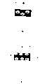
图1a-1d为于不同操作状态下由分子合成的储存单元的简化结构图。Figures 1a-1d are simplified structural diagrams of storage units synthesized from molecules under different operating states.
图2为本发明的一实施例中开关装置处于断开状态的示意图。FIG. 2 is a schematic diagram of a switch device in an off state in an embodiment of the present invention.
图3为图2中的开关装置处于接通状态时的示意图。FIG. 3 is a schematic diagram of the switch device in FIG. 2 when it is in an on state.
图4为本发明的另一实施例中开关装置处于接通状态下的示意图。FIG. 4 is a schematic diagram of a switch device in an on state in another embodiment of the present invention.
具体实施方式Detailed ways
本发明所提出及解决的问题即提供一种新的开关装置,其可具备储存功能。本发明克服了上述的问题,且多半是通过引入活性区域的方式来实现,此活性区域即电性连接在一对信号端之间。当在预定时间内于控制端与信号极之间施加一量值及极性均预先给定的电压时,此活性区域即成导电状态并电性连接两信号端。The problem proposed and solved by the present invention is to provide a new switch device which can have a storage function. The present invention overcomes the above-mentioned problems, and it is mostly realized by introducing an active region, which is electrically connected between a pair of signal terminals. When a voltage with predetermined magnitude and polarity is applied between the control terminal and the signal electrode within a predetermined time, the active area becomes conductive and electrically connects the two signal terminals.
活性区域表现出可作反复开关及储存的效能,使其应用于人眼可见的装置中。该活性区域是由分子系统制成,且在整个分子系统中分布有离子复合物。这些分布于分子系统中的离子复合物在施加电场作用下分离。The active area exhibits the performance of repeated switching and storage, making it applicable to devices visible to the human eye. The active region is made of a molecular system with ionic complexes distributed throughout the molecular system. These ionic complexes distributed in molecular systems are separated under the action of an applied electric field.
在一维空间中,活性区域分子状态的合成物表现出结构及电方面的不稳定,并能静态及动态地控制分子系统的传导性能。储存及开关的机理似乎与一维分子系统在结构及电方面的不稳定有关,并也与在外部电场的作用下分子分离和/或原子移位有关。In one-dimensional space, the composition of the molecular state of the active region exhibits structural and electrical instability, and can statically and dynamically control the conduction properties of the molecular system. The mechanism of storage and switching appears to be related to the structural and electrical instability of one-dimensional molecular systems, and also to molecular separation and/or atomic displacement under the action of an external electric field.
分子电子学的发展激发人们更详细地研究分子薄膜的电物理特性,分子薄膜的电物理特性提供了新的物理效应,并为电开关及储存应用带来了新的技术。虽然此在20世纪60年代已进行首次报导,但至今仍未有大众所普遍认同的解释。这大部分要归因于所得到的结果并不具有反复性,即便是使用了同样的化合物也是如此。The development of molecular electronics has inspired people to study the electrophysical properties of molecular thin films in more detail. The electrophysical properties of molecular thin films provide new physical effects and bring new technologies for electrical switching and storage applications. Although this was first reported in the 1960s, there is still no explanation generally accepted by the public. This is largely due to the fact that the results obtained were not reproducible, even with the same compounds.
大量不同的物质可作为分子的合成物。以下即说明此些典型的物质,其讨论于Yu H.Krieger的文章中,标题为“Structural Instability ofOne-Dimensional Systems As A Physical Principle Underlying TheFunctioning of Molecular Electronic Devices”,Journal of StructuralChemistry,Vol.40,NO.4,1999(Yu H.Krieger),可一并加以参考。A large number of different substances are available as molecular compositions. Such typical substances are illustrated below, discussed in Yu H. Krieger's article entitled "Structural Instability of One-Dimensional Systems As A Physical Principle Underlying The Functioning of Molecular Electronic Devices", Journal of Structural Chemistry, Vol.40, NO .4, 1999 (Yu H. Krieger), which may be referred to together.
许多分子储存器开关可包括一维导电分子系统,此些导电分子系统表现出结构上的不稳定(佩尔斯胁强应力,Peierls-effect)。且这些分子储存器开关往往具有S状(凹角形,reentrant)电压-电流特性并带有储存功能。此些储存器开关的电阻值可在几十欧姆至几百欧姆之间,阻值大小与开关状态有关。Many molecular storage switches can include one-dimensional conducting molecular systems that exhibit structural instability (Peierls-effect). And these molecular storage switches often have S-shaped (reentrant) voltage-current characteristics and have a storage function. The resistance value of these memory switches can be between tens of ohms and hundreds of ohms, and the resistance value is related to the state of the switch.
而此种分子系统的组织结构具有两种突出之类型。第一类为柱状线型共轭聚合物(strands of linear conjugated polymers),此结构相互之间连结弱,且其共有部分的排列组织得也差。第二类为晶体结构,其中,个体分子形成一维柱状(one-dimensional columns),且同一柱状分子间的相互作用要比不同柱状分子间的相互作用来得更活跃。近来,此两类分子系统已被综合。The organizational structure of this molecular system has two prominent types. The first type is columnar linear conjugated polymers (strands of linear conjugated polymers), which are weakly connected to each other, and the arrangement of their common parts is also poor. The second category is crystal structures, in which individual molecules form one-dimensional columns and the interactions between molecules in the same column are more active than those between molecules in different columns. Recently, these two classes of molecular systems have been synthesized.
聚合共轭系统(Ployconjugated systems)主要包括聚乙烯(polyvinylene),也就是,具有非环状共轭系统的聚合物,其中,结构的一维特征是由线型巨分子共轭机制予以标示出来。聚乙炔(polyacetylene)是此类聚合物的典型代表。其电子构造是许多其它共轭聚合物的模型。Polyconjugated systems (Ployconjugated systems) mainly include polyethylene (polyvinylene), that is, polymers with acyclic conjugated systems, wherein the one-dimensional feature of the structure is marked by the linear macromolecular conjugation mechanism. Polyacetylene is a typical representative of such polymers. Its electronic configuration is a model for many other conjugated polymers.
另一大类的分子化合物是由芳香族与杂环分子形成,此类分子化合物因分子间的π键结而具有高导电性。这样的分子系统则称为π复合物或电荷转移复合物,其结构包含绝缘一维柱状物或具有声称利于开关储存应用的电物理特性的条状物。分子电荷转移复合物是由两个分子形成的施体-受体系统;一个具有施体特性,而另一个则具有受体特性。在已确切定义且具有一维结构的复合物中,四-氰基-基-二甲烷(tetra-cyano-quino-dimethane,TCNQ)是具未饱和键结的平面分子,安置于晶体内作为平行堆迭而形成准一维系统。Another large class of molecular compounds is formed by aromatic and heterocyclic molecules, which have high conductivity due to the π bonding between molecules. Such molecular systems are called π-complexes or charge-transfer complexes, and their structures consist of insulating one-dimensional pillars or strips with electrophysical properties claimed to be beneficial for switch storage applications. Molecular charge transfer complexes are donor-acceptor systems formed by two molecules; one with donor properties and the other with acceptor properties. In well-defined complexes with a one-dimensional structure, tetra-cyano-quino-dimethylethane (TCNQ) is a planar molecule with unsaturated bonds, arranged in the crystal as a parallel stacked to form a quasi-one-dimensional system.
在另一类一维系统中,阳离子是动态无规则的。其包含具通用公式(TMTSF)2X的分子化合物。K2Pt(CN)4Br0.3×3H2O(KCP)类中的过渡金属盐也是具混合价准一维复合物中的典型代表,其如同酞菁和卟啉。而且,纯无机化合物,如NbSe3,也是很好例子来说明具准一维结构的化合物。In another class of one-dimensional systems, cations are dynamically random. It comprises molecular compounds with the general formula (TMTSF)2X . Transition metal salts in K2 Pt(CN)4 Br0.3 ×3H2 O(KCP) are also typical representatives of quasi-one-dimensional complexes with mixed valences, like phthalocyanines and porphyrins. Moreover, purely inorganic compounds, such as NbSe3 , are good examples of compounds with quasi-one-dimensional structures.
如图1a-1d所示为本发明的一实施例形成部分简化分子储存单元(MC)的分子合成物。分子合成物包括准一维(或至少结构上及电性上是各向异性的)的分子矩阵(matrix),其中,离子复合物分布在矩阵内。在上述的实施例所述的准一维系统,如聚苯乙炔(ployphenylacetylene)的聚合物共轭化合物,可用作具各向异性的分子矩阵。离子复合物可为盐,如氯化钠(NaCl)、氯化铯(CsCl),或其它任何在施加电场的作用下可分离的物质。如图1a-1d所示,在本实施例中,具各向异性的分子矩阵是由类似链状的分子以朝与电极表面相垂直的方向排列而成。然而,这些分子或各向异性的“信道”也可有其它的朝向,其只要如图1a-1d所示能够使电荷分离即可。A molecular composition forming part of a simplified molecular memory cell (MC) is shown in Figures 1a-1d for an embodiment of the present invention. The molecular composition comprises a quasi-one-dimensional (or at least structurally and electrically anisotropic) molecular matrix in which ionic complexes are distributed. The quasi-one-dimensional system described in the above examples, such as the polymer conjugated compound of polyphenylacetylene, can be used as an anisotropic molecular matrix. Ionic complexes can be salts, such as sodium chloride (NaCl), cesium chloride (CsCl), or any other species that is separable under the action of an applied electric field. As shown in FIGS. 1a-1d , in this embodiment, the anisotropic molecular matrix is formed by chain-like molecules arranged in a direction perpendicular to the electrode surface. However, these molecular or anisotropic "channels" can also have other orientations, as long as they enable charge separation as shown in Figures 1a-1d.
然而不受限于理论,以下即可确切说明分子合成物传导率变化的机理。如图1a-1d所示,分子薄膜内的电子开关,其特征在于,其存在两个稳定的状态,即一高阻抗状态(断开状态)和一低阻抗状态(接通状态)。在断开状态下的阻抗通常要高于几十MΩ。当所施加的电场强度超过一初始值时,便将开关从断开状态切换至接通状态。而在开通状态下的阻抗要低于几百Ω。当所施加的电场极性反转后,即将开关从接通状态切换回断开状态。However, without being bound by theory, the mechanism of the change in the conductivity of the molecular composite can be precisely explained as follows. As shown in Figures 1a-1d, the electronic switch in the molecular film is characterized in that it has two stable states, namely a high impedance state (off state) and a low impedance state (on state). The impedance in the off state is usually higher than tens of MΩ. When the applied electric field strength exceeds an initial value, the switch is switched from an off state to an on state. The impedance in the open state is lower than several hundred Ω. The switch is switched from the on state back to the off state when the polarity of the applied electric field is reversed.
可识别两种储存单元的操作模式:亚稳态模式(图1b)和稳态模式(图1c)。操作储存单元的稳态模式,其特征可为:在断开状态与接通状态之间作切换所用的初始电压量高(在约3-10V之间的范围内),处于接通状态下的阻抗低(低于100Ω),开关时间长(1ms以上)及储存时间长(两个月以上)。一些储存单元在储存六年后仍表现出实质未有变化的电特性。Two modes of operation of the memory cell can be identified: the metastable mode (Fig. 1b) and the steady-state mode (Fig. 1c). Steady-state mode of operation of the storage cell, which may be characterized by a high amount of initial voltage (in the range between about 3-10V) for switching between the off-state and the on-state, impedance in the on-state Low (less than 100Ω), long switching time (above 1ms) and long storage time (above two months). Some memory cells exhibited substantially unchanged electrical characteristics after six years of storage.
相反,储存单元的亚稳态模式,其特征在于,在断开状态与接通状态之间作切换所用的初始电压量低(在约0.1-0.5V之间的范围内),处于接通状态下的阻抗高(所涵盖范围广,约1kΩ~1MΩ),开关时间短(小于1μs)及储存时间短(在约10s至几小时之间)。In contrast, the metastable mode of the memory cell is characterized by a low amount of initial voltage (in the range between about 0.1-0.5V) for switching between the off-state and the on-state, in the on-state The impedance is high (covering a wide range, about 1kΩ ~ 1MΩ), the switching time is short (less than 1μs) and the storage time is short (between about 10s to several hours).
图1a即说明其断开状态,其中,假设各向异性分子矩阵本身为一良好的绝缘体,则其导电率实质上为0。如图1b所示,当施加一外电场E时,钠盐(sodium salt)则分解成钠离子及氯离子,且离子会移出其在各向异性分子矩阵内的最初位置,使得在接通状态下的导电率增至亚稳定状态。再增加所施加的电场,离子变得愈发激烈地分离开来(图1c),同时接通状态下的导电率还会进一步增长,并达至以上所说的稳定状态。而若在长时间内施加一非常大电场,则阴离子与阳离子会在电极端聚集起来(图1d),使得在接通状态下的导电率因缺乏移动电荷(在断开状态下)而急剧下降。Figure 1a illustrates the off state, where the conductivity is essentially zero, assuming that the anisotropic molecular matrix itself is a good insulator. As shown in Figure 1b, when an external electric field E is applied, the sodium salt (sodium salt) is decomposed into sodium ions and chloride ions, and the ions will move out of their original positions in the anisotropic molecular matrix, so that in the on state The lower conductivity increases to a metastable state. Further increasing the applied electric field, the ions become more and more violently separated (Fig. 1c), and at the same time the conductivity in the on-state increases further and reaches the above-mentioned steady state. However, if a very large electric field is applied for a long time, the anions and cations will gather at the electrode terminals (Figure 1d), so that the conductivity in the on state will drop sharply due to the lack of mobile charges (in the off state). .
就目前所知,在上述例子中,产生导电的电荷并非是钠离子及氯离子(离子导电),而是物质中存有电子和/或空穴。电子和/或空穴可通过称为“变射程跳跃式导电”(variable range hopping conduction)过程而在物质移动。看起来象是钠离子及氯离子在影响着电位势(potentialbarrier),以至增大了载子的移动率。然而,理论上未被理解之处,并非用以限制本说明书所要求保护的范围。As far as is known, in the above examples, the electrical charges that generate electrical conduction are not sodium ions and chloride ions (ion conduction), but electrons and/or holes in the material. Electrons and/or holes can move through matter through a process known as "variable range hopping conduction". It seems that sodium ions and chloride ions are affecting the potential barrier to increase the mobility of carriers. However, what is not understood theoretically is not intended to limit the scope of protection claimed in this specification.
如图2和3所示,在本发明的实施例中,门控(gate-controlled)开关装置即采用了如图1中所得到的观察。请参考图2,在本发明的一实施例中,可定址的开关装置20包括绝缘基板21,如玻璃基板或蓝宝石(sapphire)基板,及在基板21上形成的电极22,24,电极22,24即类似于场效应电晶体中的(FET)源极和漏极。而在电极22,24上沉积一活性层28,此活性层28即由如图1a-1d所述的那种合成物制成。在上述合成物构成的层28上沉积一类似于场效应电晶体(FET)中栅极氧化层的绝缘层27,之后便在绝缘层27上形成栅极26,该栅极26可由如铝制成。若各自在栅极26与电极22,24之间所施加的电压低于初始值时,请结合图1a-1d所示,此初始值即为将活性区域28从断开状态切换至接通状态所需的电压量,则合成物层28处于绝缘状态,且在电极22,24之间没有电流流过。As shown in FIGS. 2 and 3 , in an embodiment of the present invention, a gate-controlled switching device employs the observations obtained in FIG. 1 . Please refer to FIG. 2 , in an embodiment of the present invention, an
如图3所示,当在栅极26与电极22,24间施加所施加的栅极正电压VG高于初始值时,离子态的氯化钠复合物分解成钠离子与氯离子,且带负电荷的氯离子更加集中到栅极附近,而带正电荷的钠离子则更多集中到合成物层28与绝缘基板21间的交接面处。例如,要将装置26切换到导电状态(即接通状态),可在栅极26上施加0V电压,在电极22上施加-5V,而在电极24上可施加10V电压。As shown in Figure 3, when the positive grid voltage VG applied between the
换句话说,电场引起了化合物中的正电荷朝绝缘基板附近集聚。由上所述,这些正电荷好比促使化合物的导电,因而在活性层28上形成了导电信道,电荷可通过此导电信道而在电极22与电极24之间流通。因此,当电场施加于栅极时,装置20便切换到导电状态。活性层28的高导电状态可持续几秒,甚至几个月或几年不等,其与化合物是否处于亚稳态模式或稳态模式有关。In other words, the electric field causes positive charges in the compound to accumulate near the insulating substrate. From the above, these positive charges seem to promote the conduction of the compound, thus forming a conductive channel on the
装置20可回到并储存(restore)无导电状态(即断开状态),其可通过在栅极26与电极22,24之间施加一反向电压(或负电压)的方式实现。例如,要将装置20切换到断开状态时,可在栅极上施加-20V的电压,而在电极22,24上各自施加-5V和-10V的电压。The
因此,上述的布置方式产生了一具有储存功能的开关或一储存器开关,其可用作一储存装置或一开关装置。当装置20用作储存装置时,其写入即可通过在栅极26与电极22之间施加电压的方式来实现,而读取即通过检测电极22,24之间的导电率来实现。Thus, the arrangement described above results in a switch with storage function or a storage switch, which can be used as a storage device or a switching device. When the
请参考图4,本发明的另一实施例中,开关装置40是在图2,3所示的装置20做了些修改,使得由图1a-1d所示的合成物制成的活性层48直接设置在底端电极42与顶端电极44之间,而可省去使用基板。电极42可为一储存装置或开关装置的一行电极,而电极44为装置的一列电极。栅极46可形成于电极44的顶部,一绝缘层47设置于其间,以在栅极46与电极44间提供绝缘之用。Please refer to FIG. 4, in another embodiment of the present invention, the switching
同样,如同图2中所示的实施例,当在栅极46与电极42之间所施加的正电压VG使其在电极44上的正电势相对于电极42上来的多时,离子态的氯化钠合成物便分解成钠离子与氯离子。带负电荷的氯离子更加集中到顶端电极44附近,而带正电荷的钠离子则更多集中到底端电极42附近。因此,合成物层48的导电率增加,使得电流能在电极42与电极44之间流通。此一状态即为装置40的接通状态。Likewise, like the embodiment shown in FIG. 2, when the positive voltage VG applied between the grid 46 and the electrode 42 makes the positive potential on the electrode 44 more than that on the electrode 42, the ionic chlorine The sodium chloride compound is decomposed into sodium ions and chloride ions. Negatively charged chloride ions are more concentrated near the top electrode 44 , while positively charged sodium ions are more concentrated near the bottom electrode 42 . Accordingly, the conductivity of composite layer 48 is increased, enabling electrical current to flow between electrodes 42 and 44 . This state is the ON state of the
装置40可回到并储存(restore)其无导电状态(即断开状态),其通过在栅极46与电极42之间施加一反向电压(或负电压)的方式实现。装置40可为三接点储存装置,其中,写入周期内即在栅极46与电极42之间施加电压。装置40也可读取,其通过在电极42和电极44之间检测导电率的方式实现。
本发明已结合上述的较佳实施例来加以揭露,任何熟习此项技艺的人士均可在不违背本发明的精神及范畴下,对上述实施例进行修饰与改变。因此,本发明的权利保护范围,应如后述的申请专利范围所列。The present invention has been disclosed in conjunction with the above-mentioned preferred embodiments. Anyone skilled in the art can modify and change the above-mentioned embodiments without departing from the spirit and scope of the present invention. Therefore, the protection scope of the present invention should be listed in the scope of patent application described later.
Claims (50)
Applications Claiming Priority (2)
| Application Number | Priority Date | Filing Date | Title |
|---|---|---|---|
| US28905701P | 2001-05-07 | 2001-05-07 | |
| US60/289,057 | 2001-05-07 |
Publications (2)
| Publication Number | Publication Date |
|---|---|
| CN1515039A CN1515039A (en) | 2004-07-21 |
| CN100367528Ctrue CN100367528C (en) | 2008-02-06 |
Family
ID=23109850
Family Applications (1)
| Application Number | Title | Priority Date | Filing Date |
|---|---|---|---|
| CNB028117433AExpired - Fee RelatedCN100367528C (en) | 2001-05-07 | 2002-05-07 | Switching device with memory effect |
Country Status (6)
| Country | Link |
|---|---|
| US (2) | US6809955B2 (en) |
| EP (1) | EP1388179A1 (en) |
| JP (1) | JP4731794B2 (en) |
| KR (1) | KR100895901B1 (en) |
| CN (1) | CN100367528C (en) |
| WO (1) | WO2002091494A1 (en) |
Families Citing this family (35)
| Publication number | Priority date | Publication date | Assignee | Title |
|---|---|---|---|---|
| CN100367528C (en) | 2001-05-07 | 2008-02-06 | 先进微装置公司 | Switching device with memory effect |
| DE60233486D1 (en) | 2001-05-07 | 2009-10-08 | Advanced Micro Devices Inc | FLOATING GATE MEMORY BUILDING PART USING COMPOUND MOLECULAR MATERIAL |
| WO2002091496A2 (en)* | 2001-05-07 | 2002-11-14 | Advanced Micro Devices, Inc. | Reversible field-programmable electric interconnects |
| WO2002091495A2 (en)* | 2001-05-07 | 2002-11-14 | Coatue Corporation | Molecular memory device |
| US6873540B2 (en)* | 2001-05-07 | 2005-03-29 | Advanced Micro Devices, Inc. | Molecular memory cell |
| KR100900080B1 (en) | 2001-05-07 | 2009-06-01 | 어드밴스드 마이크로 디바이시즈, 인코포레이티드 | Memory device having self-assembled polymer film and manufacturing method thereof |
| US6858481B2 (en)* | 2001-08-13 | 2005-02-22 | Advanced Micro Devices, Inc. | Memory device with active and passive layers |
| US6768157B2 (en) | 2001-08-13 | 2004-07-27 | Advanced Micro Devices, Inc. | Memory device |
| US6838720B2 (en) | 2001-08-13 | 2005-01-04 | Advanced Micro Devices, Inc. | Memory device with active passive layers |
| US6806526B2 (en) | 2001-08-13 | 2004-10-19 | Advanced Micro Devices, Inc. | Memory device |
| WO2003017282A1 (en) | 2001-08-13 | 2003-02-27 | Advanced Micro Devices, Inc. | Memory cell |
| US7038935B2 (en)* | 2002-08-02 | 2006-05-02 | Unity Semiconductor Corporation | 2-terminal trapped charge memory device with voltage switchable multi-level resistance |
| US7442997B2 (en)* | 2002-08-28 | 2008-10-28 | Guobiao Zhang | Three-dimensional memory cells |
| US7012276B2 (en) | 2002-09-17 | 2006-03-14 | Advanced Micro Devices, Inc. | Organic thin film Zener diodes |
| US6944047B2 (en)* | 2002-12-19 | 2005-09-13 | North Carolina State University | Variable-persistence molecular memory devices and methods of operation thereof |
| WO2004064091A1 (en)* | 2003-01-09 | 2004-07-29 | Molecular Biophysics Inc. | Liquid based electronic device |
| US7049153B2 (en)* | 2003-04-23 | 2006-05-23 | Micron Technology, Inc. | Polymer-based ferroelectric memory |
| US6916696B1 (en) | 2003-11-20 | 2005-07-12 | Advanced Micro Devices, Inc. | Method for manufacturing a memory element |
| US6956761B2 (en)* | 2004-03-10 | 2005-10-18 | Micron Technology, Inc. | Method to manufacture polymer memory with copper ion switching species |
| US7773404B2 (en) | 2005-01-07 | 2010-08-10 | Invisage Technologies, Inc. | Quantum dot optical devices with enhanced gain and sensitivity and methods of making same |
| US7742322B2 (en) | 2005-01-07 | 2010-06-22 | Invisage Technologies, Inc. | Electronic and optoelectronic devices with quantum dot films |
| WO2005101530A1 (en) | 2004-04-19 | 2005-10-27 | Edward Sargent | Optically-regulated optical emission using colloidal quantum dot nanocrystals |
| US7746681B2 (en) | 2005-01-07 | 2010-06-29 | Invisage Technologies, Inc. | Methods of making quantum dot films |
| US7289353B2 (en)* | 2004-08-17 | 2007-10-30 | Spansion, Llc | Systems and methods for adjusting programming thresholds of polymer memory cells |
| JP4741359B2 (en)* | 2004-12-14 | 2011-08-03 | 株式会社半導体エネルギー研究所 | Semiconductor device |
| CA2519608A1 (en) | 2005-01-07 | 2006-07-07 | Edward Sargent | Quantum dot-polymer nanocomposite photodetectors and photovoltaics |
| CN1832464B (en)* | 2005-03-11 | 2010-09-15 | 中兴通讯股份有限公司 | Pilot distribution device of orthogonal frequency division duplex system and its method |
| DE602007003340D1 (en)* | 2006-09-26 | 2009-12-31 | Canon Kk | CONTRAPTION |
| JP5196755B2 (en)* | 2006-09-26 | 2013-05-15 | キヤノン株式会社 | device |
| JP5196815B2 (en) | 2007-03-09 | 2013-05-15 | キヤノン株式会社 | Helix-type substituted polyacetylene structure, its production method, device structure, ion transport membrane and gas separation membrane |
| WO2009017631A2 (en)* | 2007-07-26 | 2009-02-05 | The Regents Of The University Of California | Peroxide chemical sensor and sensing method |
| US7879678B2 (en)* | 2008-02-28 | 2011-02-01 | Versatilis Llc | Methods of enhancing performance of field-effect transistors and field-effect transistors made thereby |
| CN102365750B (en)* | 2009-03-27 | 2014-03-12 | 惠普开发有限公司 | Switchable junction with intrinsic diode |
| KR101110594B1 (en)* | 2010-02-09 | 2012-02-15 | 한국세라믹기술원 | Lamination Film of Memory Device and Manufacturing Method Thereof |
| CN105103291B (en)* | 2013-03-09 | 2018-01-16 | 国立研究开发法人科学技术振兴机构 | Electronic component |
Citations (6)
| Publication number | Priority date | Publication date | Assignee | Title |
|---|---|---|---|---|
| US4652894A (en)* | 1980-03-14 | 1987-03-24 | The Johns Hopkins University | Electrical organic thin film switching device switching between detectably different oxidation states |
| US5034192A (en)* | 1984-11-23 | 1991-07-23 | Massachusetts Institute Of Technology | Molecule-based microelectronic devices |
| US5849403A (en)* | 1995-09-13 | 1998-12-15 | Kabushiki Kaisha Toshiba | Organic thin film device |
| US6043510A (en)* | 1996-05-22 | 2000-03-28 | Akira Kawamoto | Molecule-doped negative-resistance device and method for manufacturing the same |
| US6060338A (en)* | 1989-01-10 | 2000-05-09 | Mitsubishi Denki Kabushiki Kaisha | Method of making a field effect transistor |
| US6180956B1 (en)* | 1999-03-03 | 2001-01-30 | International Business Machine Corp. | Thin film transistors with organic-inorganic hybrid materials as semiconducting channels |
Family Cites Families (103)
| Publication number | Priority date | Publication date | Assignee | Title |
|---|---|---|---|---|
| US2002A (en)* | 1841-03-12 | Tor and planter for plowing | ||
| US2001A (en)* | 1841-03-12 | Sawmill | ||
| JPS5012598B1 (en) | 1970-04-02 | 1975-05-13 | ||
| US3810127A (en) | 1970-06-23 | 1974-05-07 | Intel Corp | Programmable circuit {13 {11 the method of programming thereof and the devices so programmed |
| JPS5589980A (en) | 1978-11-27 | 1980-07-08 | Nec Corp | Semiconductor memory unit |
| US4267558A (en) | 1979-01-05 | 1981-05-12 | Texas Instruments Incorporated | Electrically erasable memory with self-limiting erase |
| US4371883A (en) | 1980-03-14 | 1983-02-01 | The Johns Hopkins University | Current controlled bistable electrical organic thin film switching device |
| JPS5864068A (en) | 1981-10-14 | 1983-04-16 | Agency Of Ind Science & Technol | How to write non-volatile semiconductor memory |
| US4677742A (en) | 1983-01-18 | 1987-07-07 | Energy Conversion Devices, Inc. | Electronic matrix arrays and method for making the same |
| GB2160049B (en) | 1984-05-28 | 1987-06-03 | Suwa Seikosha Kk | A non-volatile memory circuit |
| US4717673A (en)* | 1984-11-23 | 1988-01-05 | Massachusetts Institute Of Technology | Microelectrochemical devices |
| US4631562A (en) | 1985-05-31 | 1986-12-23 | Rca Corporation | Zener diode structure |
| DE3602887A1 (en) | 1986-01-31 | 1987-08-06 | Bayer Ag | NON-VOLATILE ELECTRONIC MEMORY |
| US4727514A (en) | 1986-02-11 | 1988-02-23 | Texas Instruments Incorporated | Programmable memory with memory cells programmed by addressing |
| JPH0770708B2 (en)* | 1986-03-25 | 1995-07-31 | 株式会社東芝 | Field effect transistor |
| US4834911A (en) | 1986-08-25 | 1989-05-30 | Electro-Organic Company | Intrinsically conductive and semiconductive polymers, products formed with such polymers and methods of forming same |
| DE3751376T2 (en)* | 1986-10-13 | 1995-11-16 | Canon Kk | Circuit element. |
| JPH01100788A (en) | 1987-10-13 | 1989-04-19 | Hitachi Ltd | Semiconductor integrated circuit device |
| US4839700A (en) | 1987-12-16 | 1989-06-13 | California Institute Of Technology | Solid-state non-volatile electronically programmable reversible variable resistance device |
| US5440518A (en) | 1991-06-12 | 1995-08-08 | Hazani; Emanuel | Non-volatile memory circuits, architecture and methods |
| US5136212A (en) | 1988-02-18 | 1992-08-04 | Canon Kabushiki Kaisha | Electron emitting device, electron generator employing said electron emitting device, and method for driving said generator |
| JPH0239568A (en)* | 1988-07-29 | 1990-02-08 | Olympus Optical Co Ltd | switching element |
| US5196912A (en) | 1988-10-28 | 1993-03-23 | Casio Computer Co., Ltd. | Thin film transistor having memory function and method for using thin film transistor as memory element |
| JP2636035B2 (en) | 1989-02-27 | 1997-07-30 | 松下電器産業株式会社 | Ferroelectric liquid crystal composition and ferroelectric liquid crystal display |
| EP0418504B1 (en) | 1989-07-25 | 1995-04-05 | Matsushita Electric Industrial Co., Ltd. | Organic semiconductor memory device having a MISFET structure and its control method |
| JP2502782B2 (en)* | 1990-02-15 | 1996-05-29 | 松下電器産業株式会社 | Electroplastic device for neural network and control method thereof |
| US5206525A (en) | 1989-12-27 | 1993-04-27 | Nippon Petrochemicals Co., Ltd. | Electric element capable of controlling the electric conductivity of π-conjugated macromolecular materials |
| US5272101A (en) | 1990-04-12 | 1993-12-21 | Actel Corporation | Electrically programmable antifuse and fabrication processes |
| US5552627A (en) | 1990-04-12 | 1996-09-03 | Actel Corporation | Electrically programmable antifuse incorporating dielectric and amorphous silicon interlayers |
| US5130380A (en) | 1990-05-29 | 1992-07-14 | Carew Evan B | Conductive polymers |
| JP3150331B2 (en)* | 1990-09-28 | 2001-03-26 | 株式会社東芝 | Organic thin film element |
| JPH0770731B2 (en) | 1990-11-22 | 1995-07-31 | 松下電器産業株式会社 | Electroplastic element |
| US5245543A (en) | 1990-12-21 | 1993-09-14 | Texas Instruments Incorporated | Method and apparatus for integrated circuit design |
| US5296716A (en) | 1991-01-18 | 1994-03-22 | Energy Conversion Devices, Inc. | Electrically erasable, directly overwritable, multibit single cell memory elements and arrays fabricated therefrom |
| FR2672158B1 (en) | 1991-01-24 | 1993-04-09 | Commissariat Energie Atomique | SENSOR FOR THE DETECTION OF CHEMICAL SPECIES OR PHOTONS USING A FIELD EFFECT TRANSISTOR. |
| JP3224829B2 (en) | 1991-08-15 | 2001-11-05 | 株式会社東芝 | Organic field effect device |
| GB9117680D0 (en) | 1991-08-16 | 1991-10-02 | Philips Electronic Associated | Electronic matrix array devices |
| KR100254246B1 (en) | 1991-08-19 | 2000-05-01 | 마빈 에스. 시스킨드 | Electrically erasable, directly overwritable, multibit single cell memory elements and arrays fabricated therefrom |
| US5563081A (en) | 1992-03-23 | 1996-10-08 | Rohm Co., Inc. | Method for making a nonvolatile memory device utilizing a field effect transistor having a ferroelectric gate film |
| JP2822791B2 (en) | 1992-06-30 | 1998-11-11 | 日本電気株式会社 | Semiconductor device |
| RU2071126C1 (en) | 1992-08-27 | 1996-12-27 | Кригер Юрий Генрихович | Storage element |
| US5579199A (en) | 1992-11-26 | 1996-11-26 | Sharp Kabushiki Kaisha | Non-volatile memory device and a method for producing the same |
| US5581111A (en) | 1993-07-07 | 1996-12-03 | Actel Corporation | Dielectric-polysilicon-dielectric antifuse for field programmable logic applications |
| US5818749A (en) | 1993-08-20 | 1998-10-06 | Micron Technology, Inc. | Integrated circuit memory device |
| JPH07106440A (en) | 1993-10-04 | 1995-04-21 | Hitachi Ltd | Nonvolatile semiconductor memory device and application system using the same |
| JP3467858B2 (en) | 1993-11-02 | 2003-11-17 | ソニー株式会社 | Photoelectric conversion element |
| JP4278721B2 (en) | 1994-09-30 | 2009-06-17 | テキサス インスツルメンツ インコーポレイテツド | Zener diode with high reverse breakdown voltage |
| JPH08222648A (en) | 1995-02-14 | 1996-08-30 | Canon Inc | Storage device |
| US5572472A (en) | 1995-04-14 | 1996-11-05 | Delco Electronics Corporation | Integrated zener-zap nonvolatile memory cell with programming and pretest capability |
| NO952545D0 (en) | 1995-06-23 | 1995-06-23 | Opticon As | Procedure for writing data in an optical memory |
| US5691935A (en) | 1995-07-13 | 1997-11-25 | Douglass; Barry G. | Memory element and method of operation thereof |
| EP0772244B1 (en) | 1995-11-06 | 2000-03-22 | Consorzio per la Ricerca sulla Microelettronica nel Mezzogiorno | MOS technology power device with low output resistance and low capacity and related manufacturing process |
| JP3030264B2 (en)* | 1996-05-22 | 2000-04-10 | インターナショナル・ビジネス・マシーンズ・コーポレイション | Mott transition molecular field effect transistor |
| US5761115A (en) | 1996-05-30 | 1998-06-02 | Axon Technologies Corporation | Programmable metallization cell structure and method of making same |
| US5734605A (en) | 1996-09-10 | 1998-03-31 | Motorola, Inc. | Multi-layer magnetic tunneling junction memory cells |
| DE19640239A1 (en) | 1996-09-30 | 1998-04-02 | Siemens Ag | Storage cell with polymer capacitor |
| JP3349638B2 (en) | 1996-11-15 | 2002-11-25 | シャープ株式会社 | Method and circuit for driving display device |
| KR100604960B1 (en) | 1997-03-28 | 2006-07-26 | 가부시키가이샤 히타치세이사쿠쇼 | Nonvolatile semiconductor memory device and manufacturing method thereof and semiconductor device and manufacturing method thereof |
| NO972803D0 (en) | 1997-06-17 | 1997-06-17 | Opticom As | Electrically addressable logic device, method of electrically addressing the same and use of device and method |
| IL121312A (en) | 1997-07-14 | 2001-09-13 | Technion Res & Dev Foundation | Microelectronic components, their fabrication and electronic networks comprising them |
| NO304956B1 (en) | 1997-07-22 | 1999-03-08 | Opticom As | Electrode device without and with a functional element, as well as an electrode device formed by electrode devices with functional element and applications thereof |
| NO973993L (en) | 1997-09-01 | 1999-03-02 | Opticom As | Reading memory and reading memory devices |
| SG77608A1 (en) | 1997-10-03 | 2001-01-16 | Inst Data Storage | Improvements relating to optical memories using electron trapping material |
| ATE434259T1 (en) | 1997-10-14 | 2009-07-15 | Patterning Technologies Ltd | METHOD OF MAKING AN ELECTRICAL CAPACITOR |
| WO1999028914A2 (en) | 1997-12-04 | 1999-06-10 | Axon Technologies Corporation | Programmable sub-surface aggregating metallization structure and method of making same |
| NO306529B1 (en) | 1998-01-16 | 1999-11-15 | Opticom As | Transistor |
| AU733522B2 (en) | 1998-01-28 | 2001-05-17 | Thin Film Electronics Asa | A method for generating electrical conducting and/or semiconducting structures in three dimensions, a method for erasing the same structures and an electric field generator/modulator for use with the method for generating |
| US6064589A (en) | 1998-02-02 | 2000-05-16 | Walker; Darryl G. | Double gate DRAM memory cell |
| JPH11312393A (en) | 1998-02-19 | 1999-11-09 | Sanyo Electric Co Ltd | Writing circuit for semiconductor memory |
| US5930162A (en)* | 1998-09-30 | 1999-07-27 | Motorola, Inc. | Quantum random address memory with polymer mixer and/or memory |
| GB2343308B (en) | 1998-10-30 | 2000-10-11 | Nikolai Franz Gregor Schwabe | Magnetic storage device |
| US6548843B2 (en)* | 1998-11-12 | 2003-04-15 | International Business Machines Corporation | Ferroelectric storage read-write memory |
| US6635914B2 (en) | 2000-09-08 | 2003-10-21 | Axon Technologies Corp. | Microelectronic programmable device and methods of forming and programming the same |
| US6487106B1 (en) | 1999-01-12 | 2002-11-26 | Arizona Board Of Regents | Programmable microelectronic devices and method of forming and programming same |
| CA2362283A1 (en) | 1999-02-11 | 2000-08-17 | Arizona Board Of Regents | Programmable microelectronic devices and methods of forming and programming same |
| ES2264928T3 (en) | 1999-02-12 | 2007-02-01 | Board Of Trustees Operating Michigan State University | NANOCAPSULES CONTAINING LOADED PARTICLES, THEIR USES AND PROCEDURES FOR THE PREPARATION OF THE SAME. |
| US6128214A (en) | 1999-03-29 | 2000-10-03 | Hewlett-Packard | Molecular wire crossbar memory |
| US6459095B1 (en) | 1999-03-29 | 2002-10-01 | Hewlett-Packard Company | Chemically synthesized and assembled electronics devices |
| FR2792761B1 (en) | 1999-04-21 | 2003-05-23 | St Microelectronics Sa | DEVICE FOR PROGRAMMING AN ELECTRICALLY PROGRAMMABLE NON-VOLATILE MEMORY |
| JP4491870B2 (en) | 1999-10-27 | 2010-06-30 | ソニー株式会社 | Driving method of nonvolatile memory |
| US6384427B1 (en) | 1999-10-29 | 2002-05-07 | Semiconductor Energy Laboratory Co., Ltd. | Electronic device |
| DE19959904C2 (en) | 1999-12-11 | 2002-03-14 | Edward William Schlag | Method and device for controlling an electrical current through biomolecules |
| US7194085B2 (en) | 2000-03-22 | 2007-03-20 | Semiconductor Energy Laboratory Co., Ltd. | Electronic device |
| NO315728B1 (en) | 2000-03-22 | 2003-10-13 | Thin Film Electronics Asa | Multidimensional addressing architecture for electronic devices |
| US6449184B2 (en) | 2000-06-19 | 2002-09-10 | Matsushita Electric Industrial Co., Ltd. | Method for driving semiconductor memory |
| US6403397B1 (en) | 2000-06-28 | 2002-06-11 | Agere Systems Guardian Corp. | Process for fabricating organic semiconductor device involving selective patterning |
| US7025277B2 (en) | 2000-09-25 | 2006-04-11 | The Trustees Of Princeton University | Smart card composed of organic processing elements |
| US20050101063A1 (en) | 2000-10-24 | 2005-05-12 | Tour James M. | Three-terminal field-controlled molecular devices |
| US6950331B2 (en) | 2000-10-31 | 2005-09-27 | The Regents Of The University Of California | Organic bistable device and organic memory cells |
| NO20005980L (en) | 2000-11-27 | 2002-05-28 | Thin Film Electronics Ab | Ferroelectric memory circuit and method of its manufacture |
| JP4667594B2 (en) | 2000-12-25 | 2011-04-13 | ルネサスエレクトロニクス株式会社 | Thin film magnetic memory device |
| JP2002230982A (en) | 2001-02-01 | 2002-08-16 | Mitsubishi Electric Corp | Nonvolatile semiconductor memory device |
| US6407953B1 (en) | 2001-02-02 | 2002-06-18 | Matrix Semiconductor, Inc. | Memory array organization and related test method particularly well suited for integrated circuits having write-once memory arrays |
| US6919633B2 (en) | 2001-03-07 | 2005-07-19 | Hewlett-Packard Development Company, L.P. | Multi-section foldable memory device |
| US6618295B2 (en) | 2001-03-21 | 2003-09-09 | Matrix Semiconductor, Inc. | Method and apparatus for biasing selected and unselected array lines when writing a memory array |
| CN100367528C (en) | 2001-05-07 | 2008-02-06 | 先进微装置公司 | Switching device with memory effect |
| DE60233486D1 (en) | 2001-05-07 | 2009-10-08 | Advanced Micro Devices Inc | FLOATING GATE MEMORY BUILDING PART USING COMPOUND MOLECULAR MATERIAL |
| US6873540B2 (en) | 2001-05-07 | 2005-03-29 | Advanced Micro Devices, Inc. | Molecular memory cell |
| KR100900080B1 (en) | 2001-05-07 | 2009-06-01 | 어드밴스드 마이크로 디바이시즈, 인코포레이티드 | Memory device having self-assembled polymer film and manufacturing method thereof |
| WO2002091495A2 (en) | 2001-05-07 | 2002-11-14 | Coatue Corporation | Molecular memory device |
| WO2002091496A2 (en) | 2001-05-07 | 2002-11-14 | Advanced Micro Devices, Inc. | Reversible field-programmable electric interconnects |
| WO2003017282A1 (en) | 2001-08-13 | 2003-02-27 | Advanced Micro Devices, Inc. | Memory cell |
| US6674121B2 (en)* | 2001-12-14 | 2004-01-06 | The Regents Of The University Of California | Method and system for molecular charge storage field effect transistor |
- 2002
- 2002-05-07CNCNB028117433Apatent/CN100367528C/ennot_activeExpired - Fee Related
- 2002-05-07USUS10/139,746patent/US6809955B2/ennot_activeExpired - Lifetime
- 2002-05-07KRKR1020037014468Apatent/KR100895901B1/ennot_activeExpired - Fee Related
- 2002-05-07EPEP02725937Apatent/EP1388179A1/ennot_activeWithdrawn
- 2002-05-07JPJP2002588649Apatent/JP4731794B2/ennot_activeExpired - Fee Related
- 2002-05-07WOPCT/US2002/014239patent/WO2002091494A1/enactiveSearch and Examination
- 2004
- 2004-06-21USUS10/873,069patent/US7145793B1/ennot_activeExpired - Fee Related
Patent Citations (6)
| Publication number | Priority date | Publication date | Assignee | Title |
|---|---|---|---|---|
| US4652894A (en)* | 1980-03-14 | 1987-03-24 | The Johns Hopkins University | Electrical organic thin film switching device switching between detectably different oxidation states |
| US5034192A (en)* | 1984-11-23 | 1991-07-23 | Massachusetts Institute Of Technology | Molecule-based microelectronic devices |
| US6060338A (en)* | 1989-01-10 | 2000-05-09 | Mitsubishi Denki Kabushiki Kaisha | Method of making a field effect transistor |
| US5849403A (en)* | 1995-09-13 | 1998-12-15 | Kabushiki Kaisha Toshiba | Organic thin film device |
| US6043510A (en)* | 1996-05-22 | 2000-03-28 | Akira Kawamoto | Molecule-doped negative-resistance device and method for manufacturing the same |
| US6180956B1 (en)* | 1999-03-03 | 2001-01-30 | International Business Machine Corp. | Thin film transistors with organic-inorganic hybrid materials as semiconducting channels |
Non-Patent Citations (1)
| Title |
|---|
| 有机薄膜场效应晶体管. 胡文平,刘云圻,朱道本.有机薄膜场效应晶体管,第26卷,第11期. 1997* |
Also Published As
| Publication number | Publication date |
|---|---|
| EP1388179A1 (en) | 2004-02-11 |
| JP4731794B2 (en) | 2011-07-27 |
| US6809955B2 (en) | 2004-10-26 |
| US7145793B1 (en) | 2006-12-05 |
| KR20040062446A (en) | 2004-07-07 |
| WO2002091494A1 (en) | 2002-11-14 |
| CN1515039A (en) | 2004-07-21 |
| US20020163829A1 (en) | 2002-11-07 |
| JP2005524967A (en) | 2005-08-18 |
| KR100895901B1 (en) | 2009-05-04 |
Similar Documents
| Publication | Publication Date | Title |
|---|---|---|
| CN100367528C (en) | Switching device with memory effect | |
| KR100885276B1 (en) | Floating Gate Memory Devices Using Complex Molecular Materials | |
| US6781868B2 (en) | Molecular memory device | |
| US7113420B2 (en) | Molecular memory cell | |
| US6844608B2 (en) | Reversible field-programmable electric interconnects | |
| Scott et al. | Nonvolatile memory elements based on organic materials | |
| EP1236206B1 (en) | Electrically addressable volatile and non-volatile molecular-based switching devices | |
| US7145824B2 (en) | Temperature compensation of thin film diode voltage threshold in memory sensing circuit | |
| US7336520B2 (en) | Storage device and semiconductor apparatus | |
| JP4731601B2 (en) | Resistive memory device with improved data retention and power saving | |
| KR20070040819A (en) | Polymer Memory with Variable Data Retention Times | |
| GB2410127A (en) | Polymer memory element stable to repeated read access operations | |
| Song et al. | Off-state operation of a three Terminal Ionic FET for logic-in-memory | |
| US20060118780A1 (en) | Organo-resistive memory unit | |
| KR20090090313A (en) | Memory Device and Manufacturing Method | |
| WO2009037590A2 (en) | Conducting polymer for electronic, photonic and electromechanical systems | |
| Casula | Non-volatile organic memory devices: from design to applications |
Legal Events
| Date | Code | Title | Description |
|---|---|---|---|
| C06 | Publication | ||
| PB01 | Publication | ||
| C10 | Entry into substantive examination | ||
| SE01 | Entry into force of request for substantive examination | ||
| C14 | Grant of patent or utility model | ||
| GR01 | Patent grant | ||
| C17 | Cessation of patent right | ||
| CF01 | Termination of patent right due to non-payment of annual fee | Granted publication date:20080206 |