CN100362619C - Radio Frequency Matching Coupling Network of Vacuum Reaction Chamber and Its Configuration Method - Google Patents
Radio Frequency Matching Coupling Network of Vacuum Reaction Chamber and Its Configuration MethodDownload PDFInfo
- Publication number
- CN100362619C CN100362619CCNB2005100285647ACN200510028564ACN100362619CCN 100362619 CCN100362619 CCN 100362619CCN B2005100285647 ACNB2005100285647 ACN B2005100285647ACN 200510028564 ACN200510028564 ACN 200510028564ACN 100362619 CCN100362619 CCN 100362619C
- Authority
- CN
- China
- Prior art keywords
- frequency
- reaction chamber
- vacuum reaction
- circuit
- coupling network
- Prior art date
- Legal status (The legal status is an assumption and is not a legal conclusion. Google has not performed a legal analysis and makes no representation as to the accuracy of the status listed.)
- Expired - Lifetime
Links
Images


Classifications
- H—ELECTRICITY
- H03—ELECTRONIC CIRCUITRY
- H03H—IMPEDANCE NETWORKS, e.g. RESONANT CIRCUITS; RESONATORS
- H03H7/00—Multiple-port networks comprising only passive electrical elements as network components
- H03H7/38—Impedance-matching networks
- H03H7/40—Automatic matching of load impedance to source impedance
- H—ELECTRICITY
- H01—ELECTRIC ELEMENTS
- H01J—ELECTRIC DISCHARGE TUBES OR DISCHARGE LAMPS
- H01J37/00—Discharge tubes with provision for introducing objects or material to be exposed to the discharge, e.g. for the purpose of examination or processing thereof
- H01J37/32—Gas-filled discharge tubes
- H01J37/32009—Arrangements for generation of plasma specially adapted for examination or treatment of objects, e.g. plasma sources
- H01J37/32082—Radio frequency generated discharge
- H01J37/32174—Circuits specially adapted for controlling the RF discharge
- H01J37/32183—Matching circuits
- H—ELECTRICITY
- H05—ELECTRIC TECHNIQUES NOT OTHERWISE PROVIDED FOR
- H05H—PLASMA TECHNIQUE; PRODUCTION OF ACCELERATED ELECTRICALLY-CHARGED PARTICLES OR OF NEUTRONS; PRODUCTION OR ACCELERATION OF NEUTRAL MOLECULAR OR ATOMIC BEAMS
- H05H1/00—Generating plasma; Handling plasma
- H05H1/24—Generating plasma
- H05H1/46—Generating plasma using applied electromagnetic fields, e.g. high frequency or microwave energy
Landscapes
- Physics & Mathematics (AREA)
- Engineering & Computer Science (AREA)
- Plasma & Fusion (AREA)
- Chemical & Material Sciences (AREA)
- Analytical Chemistry (AREA)
- Electromagnetism (AREA)
- Spectroscopy & Molecular Physics (AREA)
- Plasma Technology (AREA)
- Chemical Vapour Deposition (AREA)
- Drying Of Semiconductors (AREA)
Abstract
Translated fromChinese
Description
Translated fromChinese所属技术领域Technical field
本发明关于半导体或集成电路制造领域,尤其涉及一种真空反应室的射频匹配耦合网络及其配置方法。The invention relates to the field of semiconductor or integrated circuit manufacturing, in particular to a radio frequency matching coupling network of a vacuum reaction chamber and a configuration method thereof.
背景技术Background technique
真空反应室的工作原理是在真空反应室中通入反应气体,然后再对该真空反应室进行射频能量输入,该能量输入激活反应气体,在真空反应室内形成等离子体对半导体工艺件进行处理。在这个过程中,以往的技术是对真空反应室的下电极输入单一频率的射频能量,如美国相关国家标准为13.56MHz。The working principle of the vacuum reaction chamber is to pass the reaction gas into the vacuum reaction chamber, and then input radio frequency energy to the vacuum reaction chamber. The energy input activates the reaction gas, and forms plasma in the vacuum reaction chamber to process the semiconductor process parts. In this process, the previous technology is to input radio frequency energy of a single frequency to the lower electrode of the vacuum reaction chamber, such as the relevant national standard of the United States is 13.56MHz.
随着半导体工艺件等离子体处理技术的不断发展,最近双射频能量输入技术被应用于真空反应室中反应气体的激活,提高等离子体对半导体工艺件的处理效果。所谓的双射频能量输入就是将两种不等频率的射频能量同时输入真空反应室,如目前的低频2MHz和高频60MHz等不同的双频组合。With the continuous development of plasma processing technology for semiconductor process parts, dual radio frequency energy input technology has recently been applied to the activation of reactive gases in vacuum reaction chambers to improve the plasma processing effect on semiconductor process parts. The so-called dual radio frequency energy input is to input two different frequency radio frequency energy into the vacuum reaction chamber at the same time, such as the current low frequency 2MHz and high frequency 60MHz and other different dual frequency combinations.
在对真空反应室进行能量输入时,并不是所有的射频能量都能被顺利的输入,真空反应室一般具有上下电极的容性阻抗。其对于射频能量输入具有一定的反射率,因此一部分能量就不能输入造成了能量的浪费,更严重的是这部分能量被反馈回输入电路,导致输入电路发热甚至烧毁。由于对射频源而言真空反应室可以等效为一个容性阻抗的负载,因而其阻抗值是一个复数阻抗。理论证明当输入电路的阻抗值与之互为共轭复阻抗时,其反射率最低,能量能够充分输入。因此在输入网络中加入适当值的电容和电感组成与真空反应室的阻抗相共轭的匹配。这种利用电容和电感组成的输入网络被称之为射频匹配耦合网络。When energy is input to the vacuum reaction chamber, not all radio frequency energy can be smoothly input, and the vacuum reaction chamber generally has the capacitive impedance of the upper and lower electrodes. It has a certain reflectivity for RF energy input, so part of the energy cannot be input, resulting in energy waste, and what is more serious is that this part of energy is fed back to the input circuit, causing the input circuit to heat up or even burn out. Since the vacuum reaction chamber can be equivalent to a capacitive impedance load for the radio frequency source, its impedance value is a complex impedance. Theory proves that when the impedance value of the input circuit is the conjugate complex impedance, the reflectivity is the lowest and the energy can be fully input. Therefore, adding appropriate values of capacitance and inductance to the input network constitutes a conjugate match with the impedance of the vacuum reaction chamber. This input network composed of capacitors and inductors is called an RF matching coupling network.
随之产生的问题是,由于高频和低频输入同时接入真空反应室,因此其真空反应室的射频匹配耦合网络也就不可避免地相连接。高频和低频输入于一点汇集后,其部分能量不是输入真空反应室而是互相进入对方,相互烧毁对方射频源。对高频和低频输入的真空反应室的射频匹配耦合网络进行隔离,目前可以达到隔离程度为:输入对方真空反应室的射频匹配耦合网络和输入真空反应室的功率比为-20分贝(db),即为1%。The resulting problem is that since the high-frequency and low-frequency inputs are connected to the vacuum reaction chamber at the same time, the RF matching coupling network of the vacuum reaction chamber is inevitably connected. After the high-frequency and low-frequency inputs are gathered at one point, part of their energy is not input into the vacuum reaction chamber but into each other, and burns each other's RF sources. Isolate the RF matching coupling network of the high-frequency and low-frequency input vacuum reaction chamber. At present, the degree of isolation can be achieved: the power ratio of the RF matching coupling network input to the other vacuum reaction chamber and the input vacuum reaction chamber is -20 decibels (db) , which is 1%.
基于两个射频源输入频率相差比较大的思路,目前解决这一问题的方法是在两个射频匹配耦合网络的连接点之前各设置一个滤波器,在低频输入一侧设高频滤波器,在高频一侧设低频滤波器。这样就将相互输入对方射频匹配耦合网络的能量通过滤波器滤除了。Based on the idea that the input frequencies of the two RF sources are relatively large, the current solution to this problem is to set a filter before the connection point of the two RF matching coupling networks, set a high-frequency filter on the low-frequency input side, and set a high-frequency filter on the low-frequency input side. A low-frequency filter is provided on the high-frequency side. In this way, the energy input into each other's RF matching coupling network is filtered out by the filter.
这样的解决方案至少有两大缺陷。首先,直接滤除能量会造成大量的能量浪费,降低了输入效率;其次,滤除能量会导致滤波器发热。而且,这种大功率的能量滤除本身也会需要较大体积的滤波器,因此会造成设备的体积和重量增大,同时也增加了设计制造成本。Such a solution has at least two major drawbacks. First of all, directly filtering out energy will cause a lot of energy waste and reduce the input efficiency; secondly, filtering out energy will cause the filter to heat up. Moreover, such high-power energy filtering itself also requires a large-volume filter, which will increase the volume and weight of the device, and also increase the design and manufacturing costs.
发明内容Contents of the invention
本发明的目的在于提供一种真空反应室能够克服现有多重射频源之间的隔离技术问题,着重解决高频和低频射频源之间的能量互流而导致发热甚至烧毁的问题。The purpose of the present invention is to provide a vacuum reaction chamber which can overcome the technical problem of isolation between multiple radio frequency sources in the prior art, and focus on solving the problem of heat generation or even burning due to energy flow between high frequency and low frequency radio frequency sources.
本发明是通过以下技术方法实现这一目的的:一种真空反应室的射频匹配耦合网络包括:第1至第n个射频输入端口分别与第1至第n个射频源连接,每一个射频源分别具有不同的频率,以及一个将前述多个射频源能量输出到真空反应室的输出端口,其中频率依次递减,第i频率射频输入端口至输出端口之间构成第i电路,该第i电路在输出端口对输入频率中除第i频率以外的所有频率具有高阻抗;当第i电路与第i频率射频源连接后,从输出端口往第i电路方向观察测量,其具有在该第i频率下的一第一阻抗值,以及从输出端口往与前述第i电路方向相反的方向观察测量,其具有在该第i频率下的一第二阻抗值,该第一阻抗值和第二阻抗值大致共轭匹配。The present invention achieves this purpose through the following technical methods: a radio frequency matching coupling network of a vacuum reaction chamber includes: the 1st to nth radio frequency input ports are respectively connected to the 1st to nth radio frequency sources, and each radio frequency source have different frequencies respectively, and an output port that outputs the energy of the aforementioned multiple radio frequency sources to the vacuum reaction chamber, wherein the frequency decreases successively, and the i-th circuit is formed between the i-th frequency radio frequency input port and the output port, and the i-th circuit is in The output port has high impedance to all frequencies except the i-th frequency in the input frequency; when the i-th circuit is connected to the i-th frequency radio frequency source, observe and measure from the output port to the i-th circuit direction, which has the i-th frequency A first impedance value of , and the observation and measurement from the output port to the direction opposite to the direction of the aforementioned i-th circuit has a second impedance value at the i-th frequency, and the first impedance value and the second impedance value are approximately Conjugate matching.
其中相邻的两个频率中,高的频率与低的频率大小之比大于等于5。所述的每一路电路至少包括:电容、电感和接地电容,其中电容和电感串接,再与接地电容相串接。每一路电路的接法可以是L型、倒L型、T型或π型。n为大于或等于2的自然数,i为大于或等于2且小于或等于n的某一个自然数。所述的真空反应室是等离子体沉积设备或等离子体刻蚀设备。Among the two adjacent frequencies, the ratio of the high frequency to the low frequency is greater than or equal to 5. Each said circuit at least includes: a capacitor, an inductor and a grounding capacitor, wherein the capacitor and the inductor are connected in series, and then connected in series with the grounding capacitor. The connection of each circuit can be L-type, inverted L-type, T-type or π-type. n is a natural number greater than or equal to 2, and i is a certain natural number greater than or equal to 2 and less than or equal to n. The vacuum reaction chamber is plasma deposition equipment or plasma etching equipment.
本发明另一技术方案是:一种真空反应室的射频匹配耦合网络包括:与第一频率射频源连接的第一频率射频输入端口,与第二频率射频源连接的第二频率射频输入端口,以及一个将多重射频源能量输出到真空反应室的输出端口,其中第一频率高于第二频率, 第一频率射频输入端口至输出端口之间构成第一电路,该第一电路在输出端口对第二频率具有高阻抗;第二频率射频输入端口至输出端口之间构成第二电路,该第二电路在输出端口对第一频率具有高阻抗;当第一电路与第一频率射频源连接后,从输出端口往第一电路方向观察测量,其具有在该第一频率下的一第一阻抗值,以及从输出端口往与前述第一电路方向相反的方向观察测量,其具有在该第一频率下的一第二阻抗值,该第一阻抗值和第二阻抗值大致共轭匹配。Another technical solution of the present invention is: a radio frequency matching coupling network of a vacuum reaction chamber includes: a first frequency radio frequency input port connected to a first frequency radio frequency source, a second frequency radio frequency input port connected to a second frequency radio frequency source, and an output port that outputs energy from multiple radio frequency sources to the vacuum reaction chamber, wherein the first frequency is higher than the second frequency, and a first circuit is formed between the first frequency radio frequency input port and the output port, and the first circuit is connected between the output port and the output port The second frequency has high impedance; a second circuit is formed between the second frequency radio frequency input port and the output port, and the second circuit has high impedance to the first frequency at the output port; when the first circuit is connected to the first frequency radio frequency source , viewing the measurement from the output port toward the first circuit, which has a first impedance value at the first frequency, and viewing the measurement from the output port in a direction opposite to the direction of the first circuit, which has a value at the first A second impedance value at a frequency, the first impedance value and the second impedance value are approximately conjugate matched.
其中,所述的第一电路和第二电路至少包括:电容、电感和接地电容,其中电容和电感串接,再与接地电容相串接。所述的电容和接地电容全部或部分为可变电容。所述的每一路电路的接法可以是L型、倒L型、T型或π型。所述的第一频率的大小与第二频率的大小之比为5或大于5。第一电路输出端口与真空反应室之间还串接有一个导电连接体,该导电连接体的顶端可为一个分支或多个分支,所述一个分支或多个分支与真空反应室的下电极连接。第二电路的电感靠近输出端口一侧的电感线圈绕线的线与线之间的距离较靠近第二频率射频输入端口一侧的电感线圈绕线的线与线之间的距离大。所述的真空反应室是等离子体沉积设备或等离子体刻蚀设备。Wherein, the first circuit and the second circuit at least include: a capacitor, an inductor and a grounding capacitor, wherein the capacitor and the inductor are connected in series, and then connected in series with the grounding capacitor. All or part of the capacitors and grounding capacitors are variable capacitors. The connection of each circuit can be L-type, inverted-L-type, T-type or π-type. The ratio of the magnitude of the first frequency to the magnitude of the second frequency is 5 or greater than 5. A conductive connecting body is also connected in series between the output port of the first circuit and the vacuum reaction chamber. connect. The distance between the wires of the inductance coil on the side near the output port of the inductance of the second circuit is larger than the distance between the wires of the inductance coil near the second frequency radio frequency input port. The vacuum reaction chamber is plasma deposition equipment or plasma etching equipment.
本发明的另一目的在于提供一种解决高频和低频射频源之间的能量互流而导致发热甚至烧毁的问题的真空反应室的射频匹配耦合网络的配置方法。Another object of the present invention is to provide a method for configuring a radio frequency matching coupling network of a vacuum reaction chamber that solves the problem of heating or even burning due to the energy flow between high frequency and low frequency radio frequency sources.
为了实现这一目的,本发明提供了如下技术方案:一种真空反应室的射频匹配耦合网络的配置方法,包括以下步骤:a.设置第一频率射频输入端口与第一频率射频源连接,设置第二频率射频输入端口与第二频率射频源连接,以及设置一个输出端口将多重射频源能量输出到真空反应室,其中第一频率高于第二频率;b.在第一频率射频输入端口至输出端口之间构成第一电路,该第一电路在输出端口对第二频率具有高阻抗;c.在第二频率射频输入端口至输出端口之间构成第二电路,该第二电路在输出端口对第一频率具有高阻抗;当第一电路与第一频率射频源连接后,从输出端口往第一电路方向观察测量,其具有在该第一频率下的一第一阻抗值,以及从输出端口往与前述第一电路方向相反的方向观察测量,其具有在该第一频率下的一第二阻抗值,该第一阻抗值和第二阻抗值大致共轭匹配。In order to achieve this goal, the present invention provides the following technical solution: a method for configuring a radio frequency matching coupling network of a vacuum reaction chamber, comprising the following steps: a. setting the first frequency radio frequency input port to be connected to the first frequency radio frequency source, setting The second frequency radio frequency input port is connected with the second frequency radio frequency source, and an output port is set to output the energy of multiple radio frequency sources to the vacuum reaction chamber, wherein the first frequency is higher than the second frequency; b. at the first frequency radio frequency input port to A first circuit is formed between the output ports, and the first circuit has a high impedance to the second frequency at the output port; c. a second circuit is formed between the second frequency radio frequency input port and the output port, and the second circuit is at the output port It has high impedance to the first frequency; when the first circuit is connected to the first frequency radio frequency source, observe and measure from the output port to the first circuit direction, which has a first impedance value at the first frequency, and from the output The port is viewed and measured in a direction opposite to the direction of the first circuit, and has a second impedance value at the first frequency, and the first impedance value and the second impedance value are approximately conjugate matched.
其中,所述的第一电路和第二电路至少包括:电容、电感和接地电容,其中电容和电感串接,再与接地电容相串接。所述的电容和接地电容全部或部分为可变电容。每一路电路的接法可以是L型、倒L型、T型或π型。所述的第一频率的大小与第二频率的大小之比为5或大于5。所述的第一电路输出端口与真空反应室之间还串接有一个导电连接体,该导电连接体的顶端可为一个分支或多个分支,所述一个分支或多个分支与真空反应室的下电极连接。第二电路的电感靠近输出端口一侧的电感线圈绕线的线与线之间的距离较靠近第二频率射频输入端口一侧的电感线圈绕线的线与线之间的距离大。所述的真空反应室是等离子体沉积设备或等离子体刻蚀设备。Wherein, the first circuit and the second circuit at least include: a capacitor, an inductor and a grounding capacitor, wherein the capacitor and the inductor are connected in series, and then connected in series with the grounding capacitor. All or part of the capacitors and grounding capacitors are variable capacitors. The connection of each circuit can be L-type, inverted L-type, T-type or π-type. The ratio of the magnitude of the first frequency to the magnitude of the second frequency is 5 or greater than 5. A conductive connecting body is also connected in series between the first circuit output port and the vacuum reaction chamber, and the top of the conductive connecting body can be one or more branches, and the one or more branches are connected to the vacuum reaction chamber. The lower electrode connection. The distance between the wires of the inductance coil on the side near the output port of the inductance of the second circuit is larger than the distance between the wires of the inductance coil near the second frequency radio frequency input port. The vacuum reaction chamber is plasma deposition equipment or plasma etching equipment.
本发明通过设置匹配电路使得匹配电路的阻抗与真空反应室的阻抗相匹配,取得最佳的能量输入比率,提高了能量输入效率,减少了电路热量的产生。同时本发明巧妙利用了构成匹配网络的部件的阻抗值的组合,使其分别形成高通和低通滤波器。利用电路的阻抗值引导能量的输入方向。充分利用了输入能量,避免了浪费。同时避免高频和低频射频源之间的能量互流而导致发热甚至烧毁。由于本发明结构合理,采用了线与线间距不等距的电感设计,降低了电感的寄生电容,在避免电感发热的同时保持了电感设计的紧凑性。本发明重量轻、损耗小,不需要水冷,从而节省了制造和使用成本。The invention sets the matching circuit so that the impedance of the matching circuit matches the impedance of the vacuum reaction chamber to obtain the best energy input ratio, improve the energy input efficiency, and reduce the generation of circuit heat. At the same time, the present invention skillfully utilizes the combination of the impedance values of the parts constituting the matching network to form high-pass and low-pass filters respectively. Use the impedance value of the circuit to guide the input direction of energy. The input energy is fully utilized and waste is avoided. At the same time, avoid energy mutual flow between high-frequency and low-frequency radio frequency sources, which may cause heat generation or even burn out. Due to the reasonable structure of the invention, the inductance design with unequal spacing between lines is adopted, the parasitic capacitance of the inductance is reduced, and the compactness of the inductance design is maintained while avoiding the heating of the inductance. The invention has the advantages of light weight, small loss and no need of water cooling, thereby saving manufacturing and use costs.
附图说明Description of drawings
图1为本发明的真空反应室的射频匹配耦合网络结构示意图。FIG. 1 is a schematic diagram of the radio frequency matching coupling network structure of the vacuum reaction chamber of the present invention.
图2为应用本发明的真空反应室系统从低频视角观察的示意图。FIG. 2 is a schematic diagram of a vacuum reaction chamber system applied to the present invention observed from a low-frequency perspective.
图3为应用本发明的真空反应室系统从高频视角观察的示意图。FIG. 3 is a schematic diagram of a vacuum reaction chamber system applied to the present invention observed from a high-frequency perspective.
图4为用于本发明射频匹配耦合网络中的电感结构示意图。FIG. 4 is a schematic diagram of the structure of the inductor used in the radio frequency matching coupling network of the present invention.
图5为本发明一个具有多射频输入的射频匹配耦合网络的示意图。FIG. 5 is a schematic diagram of a radio frequency matching coupling network with multiple radio frequency inputs according to the present invention.
图6为用于本发明射频匹配耦合网络中的每一电路的各种连接方式示意图。FIG. 6 is a schematic diagram of various connection modes for each circuit in the radio frequency matching coupling network of the present invention.
具体实施方式Detailed ways
首先请参阅图1,图1是本发明的真空反应室的射频匹配耦合网络结构示意图。在图1中,本发明的实施例具有两个射频输入,一个为高频输入部分,另一个是低频输入部分。整个射频匹配耦合网络具有三个端口,其中两个为输入端口,即与高频射频源连接的高频输入端口和与低频射频源连接的低频输入端口,以及一个将多重射频源能量输出到真空反应室的射频输出端口。该真空反应室的射频匹配耦合网络可以分为低频部分和高频部分,这两部分通过一个连接点结合于输出端口。高频部分由一个接地的电容C1’,一个电容C2’和一个电感L’构成;低频部分的结构为低频输出一端通过一个电容C1接地,另一端连接一个电容C2,该电容串接一个电感L,通过该电感L连接到输出端口。在低频部分,由电感L、电容C1和电容C2构成了一个低通滤波器。Please refer to FIG. 1 first. FIG. 1 is a schematic structural diagram of a radio frequency matching coupling network of a vacuum reaction chamber according to the present invention. In Fig. 1, the embodiment of the present invention has two radio frequency inputs, one is a high frequency input section and the other is a low frequency input section. The entire RF matching coupling network has three ports, two of which are input ports, namely the high-frequency input port connected to the high-frequency RF source and the low-frequency input port connected to the low-frequency RF source, and one outputting the energy of multiple RF sources to the vacuum The RF output port of the reaction chamber. The radio frequency matching coupling network of the vacuum reaction chamber can be divided into a low frequency part and a high frequency part, and the two parts are combined with an output port through a connection point. The high-frequency part is composed of a grounded capacitor C1', a capacitor C2' and an inductor L'; the structure of the low-frequency part is that one end of the low-frequency output is grounded through a capacitor C1, and the other end is connected to a capacitor C2, which is connected in series with an inductor L , connected to the output port through this inductor L. In the low frequency part, a low-pass filter is formed by the inductor L, the capacitor C1 and the capacitor C2.
在高频部分,由电感L′、接地电容C1′和电容C2′构成了一个高通滤波器。在高频输入的频率远高于低频输入的频率的情况下,即高频输入至少为低频输入20倍的情况下,由于高通滤波器的特性以及高频输入时真空反应室的阻抗特性,决定了高频部分只需要很小的电感值就可以使整个匹配耦合网络与真空反应室实现阻抗共轭。因此,在高频部分也可以不设专门的电感器,与之相对应处由一片作连接导线用的导电片以及由射频输出端至真空反应室下电极的导电连接体构成。利用导电片及导电连接体的自感值来等效一个电感。在这种情况下,接地电容C1’由导电片及导电连接体对地产生的寄生电容来替代。因为寄生电容C1’和电感L’不易调节且值很小,因此在高频部分中电容C2’可被设为可变电容以调整电路的阻抗。In the high-frequency part, a high-pass filter is formed by the inductor L', the grounding capacitor C1' and the capacitor C2'. When the frequency of high-frequency input is much higher than that of low-frequency input, that is, when the high-frequency input is at least 20 times that of low-frequency input, due to the characteristics of the high-pass filter and the impedance characteristics of the vacuum reaction chamber at high-frequency input, it is determined In addition to the high frequency part, only a small inductance value can make the entire matching coupling network and the vacuum reaction chamber realize impedance conjugation. Therefore, there may not be a special inductor in the high-frequency part, and the corresponding part is composed of a conductive sheet for connecting wires and a conductive connection body from the radio frequency output terminal to the lower electrode of the vacuum reaction chamber. Use the self-inductance value of the conductive sheet and the conductive connecting body to equivalent an inductance. In this case, the ground capacitance C1' is replaced by the parasitic capacitance generated by the conductive sheet and the conductive connecting body to the ground. Because the parasitic capacitance C1' and the inductance L' are not easy to adjust and their values are very small, the capacitance C2' can be set as a variable capacitance in the high frequency part to adjust the impedance of the circuit.
根据高频和低频部分的频率可以估算出电容和电感的大小,也可以通过对电容C1的值进行选择来获得较为理想的阻抗值。此外这些由电容和电感组成的网络本身具有复阻抗,加上电路部件和导线本身的电阻,选择调节匹配耦合网络中器件的值就可以使低频部分与低频射频源连接后,从输出端口往低频部分方向观察测量,其具有在低频下的一个阻抗值,以及从输出端口往低频部分的反方向观察测量具有在低频下的另一阻抗值,该两个阻抗值大致共轭匹配(因为,实际使用过程中,两个阻抗值不可能百分之百地共轭匹配)。当高频部分与高频射频源连接后,从输出端口往高频部分方向观察测量,其具有在高频下的一个阻抗值,以及从输出端口往高频部分的反方向观察测量具有在高频下的另一阻抗值,该两个阻抗值也大致共轭匹配。The size of the capacitor and the inductor can be estimated according to the frequency of the high-frequency and low-frequency parts, and an ideal impedance value can also be obtained by selecting the value of the capacitor C1. In addition, these networks composed of capacitors and inductors have complex impedances, plus the resistance of the circuit components and wires themselves, the selection and adjustment of the value of the devices in the matching coupling network can make the low-frequency part connected to the low-frequency RF source, from the output port to the low-frequency A portion of the direction-viewing measurement that has one impedance value at low frequencies, and the opposite direction viewing measurement from the output port toward the low-frequency portion has another impedance value at low frequencies that are approximately conjugate matched (because, in practice During use, the two impedance values cannot be 100% conjugate matched). When the high-frequency part is connected to the high-frequency radio frequency source, observe and measure from the output port to the high-frequency part, which has an impedance value at high frequency, and observe and measure from the output port to the opposite direction of the high-frequency part. The two impedance values are also roughly conjugate matched.
请参阅图2,图2为应用本发明的真空反应室系统从低频视角观察的示意图。在图2中的真空反应室系统包括三大部分:低频射频源和高频射频源(未图示)、射频匹配耦合网络、以及真空反应室。低频射频源连接射频匹配耦合网络。射频匹配耦合网络中包含有高频和低频部分。射频匹配耦合网络与真空反应室连接,将射频能量提供给真空反应室。真空反应室由上电极1和下电极2组成,在下电极2上方放置有待处理的半导体工艺件3,在上下电极之间形成等离子体4对半导体工艺件3进行处理。在射频匹配耦合网络与真空反应室的下电极2连接导线的靠近下电极2的一端,有多个分支的导电连接体5连接到下电极2上。这个导电连接体5用来作为等效阻抗的一部分以补充射频匹配耦合网络阻抗值的不足。Please refer to FIG. 2 . FIG. 2 is a schematic diagram of the vacuum reaction chamber system applied to the present invention observed from a low-frequency perspective. The vacuum reaction chamber system in FIG. 2 includes three parts: a low frequency radio frequency source and a high frequency radio frequency source (not shown), a radio frequency matching coupling network, and a vacuum reaction chamber. The low frequency radio frequency source is connected with the radio frequency matching coupling network. The RF matching coupling network contains high frequency and low frequency parts. The radio frequency matching coupling network is connected with the vacuum reaction chamber to provide radio frequency energy to the vacuum reaction chamber. The vacuum reaction chamber is composed of an
在图2的射频匹配耦合网络中,低频射频能量由低频射频源产生后,经过由电容C2和电感L组成的电路到达输出端口,这时射频输出具有两个支路可选,即输入真空反应室或者输入高频部分(即,由寄生电容C1’、电容C2’和电感L’组成的支路)。高频部分由寄生电容C1’、电容C2’和电感L’构成。由于高频部分的寄生电容C1’、电容C2’和电感L’经过设定。对于低频射频输入而言,该输入高频部分支路的阻抗值远远大于真空反应室的阻抗值。因此,低频射频源的绝大部分能量输入了真空反应室。进一步的,可以通过适当选择电容C2’的值,使输入高频部分的能量小于2%。In the RF matching coupling network in Figure 2, after the low-frequency RF energy is generated by the low-frequency RF source, it reaches the output port through a circuit composed of capacitor C2 and inductor L. At this time, the RF output has two optional branches, that is, the input vacuum response Chamber or input high frequency part (that is, the branch composed of parasitic capacitance C1', capacitance C2' and inductance L'). The high frequency part is composed of parasitic capacitance C1', capacitance C2' and inductance L'. Because the parasitic capacitance C1', capacitance C2' and inductance L' of the high frequency part are set. For the low-frequency radio frequency input, the impedance value of the input high-frequency part branch is much larger than the impedance value of the vacuum reaction chamber. Therefore, most of the energy of the low-frequency RF source is input into the vacuum reaction chamber. Further, by properly selecting the value of the capacitor C2', the energy input into the high frequency part is less than 2%.
请参阅图3,图3为应用本发明的真空反应室系统从高频视角观察的示意图。在图3的射频匹配耦合网络中,高频射频能量由高频射频源产生后,经过由电容C2’和电感L’组成的电路到达输出端口,这时射频输出具有两个支路可选,即输入真空反应室或者输入低频部分(即,由寄生电容C1、电容C2和电感L组成的支路)。低频部分由电容C2、电感L和电容C1构成,其中,电感L和电容C2串接后接入低频射频源(未图示),而电容C1一端连接电容C2、另一端接地。通过这样的电路结构配置,加上对电容和电感值的估算,再经过调整电容的值,可以使得对于高频射频输入而言,该输入低频部分支路的阻抗值远远大于真空反应室的阻抗值,因此,绝大部分高频射频源的能量输入了真空反应室。进一步的,可以通过适当调节电容C1的值,使输入低频部分的能量小于2%。Please refer to FIG. 3 . FIG. 3 is a schematic view of the vacuum reaction chamber system applied in the present invention viewed from a high-frequency perspective. In the RF matching coupling network in Figure 3, after the high-frequency RF energy is generated by the high-frequency RF source, it reaches the output port through a circuit composed of capacitor C2' and inductor L'. At this time, the RF output has two optional branches. That is, input to a vacuum reaction chamber or input to a low frequency part (ie, a branch circuit composed of parasitic capacitance C1 , capacitance C2 and inductance L). The low-frequency part is composed of capacitor C2, inductor L and capacitor C1, wherein the inductor L and capacitor C2 are connected in series to a low-frequency radio frequency source (not shown), and one end of capacitor C1 is connected to capacitor C2 and the other end is grounded. Through such a circuit structure configuration, plus the estimation of the capacitance and inductance value, and then adjusting the value of the capacitance, it can make the impedance value of the input low-frequency part branch far greater than that of the vacuum reaction chamber for the high-frequency radio frequency input. Impedance value, therefore, most of the energy of the high-frequency RF source is input into the vacuum reaction chamber. Further, by properly adjusting the value of the capacitor C1, the energy input to the low frequency part is less than 2%.
以上所述的电容和电感全部或部分是可变的,且电容和电感串接位置也可以有各种变化。电容和电感可以是一个也可以是多个。All or part of the capacitors and inductors mentioned above are variable, and the serial connection positions of the capacitors and inductors can also be changed in various ways. There can be one or more capacitors and inductors.
本发明巧妙利用了为了构成与真空反应室产生共轭复阻抗部件的组合,利用电路的自身相互隔离的功能引导能量的输入方向。The present invention skillfully utilizes the combination of the components that generate conjugate complex impedance with the vacuum reaction chamber, and utilizes the mutual isolation function of the circuit itself to guide the input direction of energy.
对于使用高频射频功率较大的情形,即便是仅有小于2%的能量输入了低频部分,其对于低频部分的部件的损害也是明显的。特别是电感L,因为高频输入能够在电感L的线与线之间产生对地的寄生电容,进一步增大电感L的阻抗,大量能量集中消耗在电感L上使其温度迅速上升,直至L被烧毁。For the case of using high-frequency radio frequency power, even if only less than 2% of the energy is input into the low-frequency part, the damage to the components of the low-frequency part is obvious. Especially the inductor L, because high-frequency input can generate parasitic capacitance to the ground between the lines of the inductor L, which further increases the impedance of the inductor L, and a large amount of energy is concentrated on the inductor L, causing its temperature to rise rapidly until L was burned.
本发明为了解决这一问题,一种办法是将电感器L的线与线距离d变大,这样寄生电容值就会显著下降,避免了电感器L上的能量集中。但这与本发明的匹配电路小型化的目标不相一致。实际上只有接近高频输入一端的电感线圈需要减小寄生电容,另一端的电感线圈由于接近高频输入端已经消耗了部分能量,因此不至于被烧毁,也就没有必要将其线与线距离d变大。故,本发明的一个较佳实施例,请参考图4,是将电感器L接近输出端口或高频输入的一端的线与线的距离d拉大,而将电感器L接近低频输入端口的另一端的线与线的距离d保持不变。这样就形成了一种具有不等距的线与线的电感器L。In order to solve this problem in the present invention, one method is to increase the line-to-line distance d of the inductor L, so that the parasitic capacitance value will be significantly reduced, and energy concentration on the inductor L can be avoided. But this is inconsistent with the goal of miniaturization of the matching circuit of the present invention. In fact, only the inductance coil close to the high-frequency input end needs to reduce the parasitic capacitance, and the inductance coil at the other end has already consumed part of the energy due to its proximity to the high-frequency input end, so it will not be burned, and there is no need to keep the line-to-line distance d becomes larger. Therefore, a preferred embodiment of the present invention, please refer to FIG. 4, is to increase the distance d between the line and the line of the inductor L close to the output port or the high-frequency input end, and the inductor L is close to the low-frequency input port. The line-to-line distance d at the other end remains constant. This forms an inductor L with unequal line-to-line spacing.
本发明所述的真空反应室包括使用等离子体处理半导体工艺件的各种设备,例如,等离子体沉积设备、等离子体刻蚀设备等。The vacuum reaction chamber of the present invention includes various equipment for processing semiconductor process parts using plasma, for example, plasma deposition equipment, plasma etching equipment, and the like.
本发明的构思也可以应用在具有多个射频输入的真空反应室中,在该实施例中,真空反应室的射频匹配耦合网络包括n(n为大于或等于2的自然数)个射频输入端口,该第1至第n个射频输入端口分别与第1至第n个射频源连接,每一个射频源分别具有不同的频率,以及一个将前述多个射频源能量输出到真空反应室的输出端口,其中频率依次递减,第i频率射频输入端口至输出端口之间构成第i电路,该第i电路在输出端口对输入频率中除第i频率以外的所有频率具有高阻抗;当第i电路与第i频率射频源连接后,从输出端口往第i电路方向观察测量,其具有在该第i频率下的一第一阻抗值,以及从输出端口往与前述第i电路方向相反的方向观察测量,其具有在该第i频率下的一第二阻抗值,该第一阻抗值和第二阻抗值大致共轭匹配。The concept of the present invention can also be applied in a vacuum reaction chamber with multiple radio frequency inputs. In this embodiment, the radio frequency matching coupling network of the vacuum reaction chamber includes n (n is a natural number greater than or equal to 2) radio frequency input ports, The 1st to nth radio frequency input ports are respectively connected to the 1st to nth radio frequency sources, each radio frequency source has a different frequency, and an output port for outputting the energy of the aforementioned multiple radio frequency sources to the vacuum reaction chamber, Wherein the frequency decreases successively, and the i-th circuit is formed between the i-th frequency radio frequency input port and the output port, and the i-th circuit has high impedance to all frequencies except the i-th frequency in the input frequency at the output port; when the i-th circuit and the i-th frequency After the i-frequency radio frequency source is connected, observe and measure from the output port to the direction of the i-th circuit, which has a first impedance value at the i-th frequency, and observe and measure from the output port to the direction opposite to the direction of the aforementioned i-th circuit, It has a second impedance value at the ith frequency, and the first impedance value and the second impedance value are substantially conjugate matched.
其中相邻的两个频率中,高的频率与低的频率大小之比大于等于5。所述的每一路电路至少包括:电容、电感和接地电容,其中电容和电感串接,再与接地电容相串接。每一路电路的接法可以是L型、倒L型、T型或π型。所述的真空反应室是等离子体沉积设备或等离子体刻蚀设备。Among the two adjacent frequencies, the ratio of the high frequency to the low frequency is greater than or equal to 5. Each said circuit at least includes: a capacitor, an inductor and a grounding capacitor, wherein the capacitor and the inductor are connected in series, and then connected in series with the grounding capacitor. The connection of each circuit can be L-type, inverted L-type, T-type or π-type. The vacuum reaction chamber is plasma deposition equipment or plasma etching equipment.
请参阅图5,图5为本发明一个多射频输入实施例的示意图。在该实施例中的真空反应室的射频匹配耦合网络包括:第1至第n个射频输入端口,即图5中的p1至pn,分别与第1至第n个射频源连接,每一个射频源分别具有不同的频率,从f1至fn。以及一个将前述多个射频源能量输出到真空反应室的输出端口,其中频率依次递减,即图5中的f1>--->fi--->fn。其中相邻的两个频率中,高的频率与低的频率大小之比大于等于5。Please refer to FIG. 5 . FIG. 5 is a schematic diagram of a multi-radio frequency input embodiment of the present invention. The radio frequency matching coupling network of the vacuum reaction chamber in this embodiment includes: the 1st to nth radio frequency input ports, that is, p1 to pn in Figure 5, are respectively connected to the 1st to nth radio frequency sources, and each radio frequency The sources respectively have different frequencies from f1 to fn. And an output port for outputting energy of the aforementioned multiple radio frequency sources to the vacuum reaction chamber, wherein the frequency decreases successively, that is, f1>--->fi--->fn in FIG. 5 . Among the two adjacent frequencies, the ratio of the high frequency to the low frequency is greater than or equal to 5.
第i频率射频输入端口至输出端口之间构成第i电路,该第i电路在输出端口对输入频率中除第i频率fi以外的所有频率具有高阻抗;An i-th circuit is formed between the i-th frequency radio frequency input port and the output port, and the i-th circuit has high impedance to all frequencies except the i-th frequency fi in the input frequency at the output port;
当第i电路与第i频率射频源连接后,从输出端口往第i电路方向观察测量,其具有在该第i频率下的一第一阻抗值,以及从输出端口往与前述第i电路方向相反的方向观察测量,其具有在该第i频率下的一第二阻抗值,该第一阻抗值和第二阻抗值大致共轭匹配。After the i-th circuit is connected to the i-th frequency radio frequency source, observe and measure from the output port to the i-th circuit direction, which has a first impedance value at the i-th frequency, and from the output port to the aforementioned i-th circuit direction The opposite direction is observed for measurement, which has a second impedance value at the ith frequency, and the first impedance value and the second impedance value are substantially conjugate matched.
如图5所示的每一路电路至少包括:电容、电感和接地电容,其中电容和电感串接,再与接地电容相串接。这些电容和电感可以是一个也可以是多个串接而成,连接顺序也可互相交换。Each circuit shown in FIG. 5 at least includes: a capacitor, an inductor, and a grounding capacitor, wherein the capacitor and the inductor are connected in series, and then connected in series with the grounding capacitor. One or more of these capacitors and inductors can be connected in series, and the connection sequence can also be interchanged.
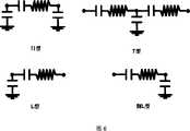
如图6所示,本发明的每一电路至少包括:电容、电感和接地电容,其中电容和电感串接,再与接地电容相串接,且电容、电感和接地电容具有各种连接方式的变形,如L型、倒L型、T型或π型。。As shown in Figure 6, each circuit of the present invention at least includes: capacitance, inductance and ground capacitance, wherein the capacitance and inductance are connected in series, and then connected in series with the ground capacitance, and the capacitance, inductance and ground capacitance have various connection modes Deformation, such as L-shape, inverted-L-shape, T-shape or π-shape. .
以上介绍的仅仅是基于本发明的几个较佳实施例,并不能以此来限定本发明的范围。任何对本发明的装置作本技术领域内熟知的部件的替换、组合、分立,以及对本发明实施步骤作本技术领域内熟知的等同改变或替换均不超出本发明的揭露以及保护范围。The above introductions are only based on several preferred embodiments of the present invention, and should not limit the scope of the present invention. Any replacement, combination, and separation of components known in the technical field to the device of the present invention, as well as equivalent changes or replacements to the implementation steps of the present invention that are well known in the technical field will not exceed the disclosure and protection scope of the present invention.
Claims (26)
Priority Applications (4)
| Application Number | Priority Date | Filing Date | Title |
|---|---|---|---|
| CNB2005100285647ACN100362619C (en) | 2005-08-05 | 2005-08-05 | Radio Frequency Matching Coupling Network of Vacuum Reaction Chamber and Its Configuration Method |
| US11/350,022US7868556B2 (en) | 2005-08-05 | 2006-02-08 | RF matching network of a vacuum processing chamber and corresponding configuration methods |
| JP2006213916AJP2007080811A (en) | 2005-08-05 | 2006-08-04 | Radio frequency (rf) matching network for vacuum reaction chamber and method of arranging same |
| US12/987,538US8334657B2 (en) | 2005-08-05 | 2011-01-10 | RF matching network of a vacuum processing chamber and corresponding configuration methods |
Applications Claiming Priority (1)
| Application Number | Priority Date | Filing Date | Title |
|---|---|---|---|
| CNB2005100285647ACN100362619C (en) | 2005-08-05 | 2005-08-05 | Radio Frequency Matching Coupling Network of Vacuum Reaction Chamber and Its Configuration Method |
Publications (2)
| Publication Number | Publication Date |
|---|---|
| CN1909184A CN1909184A (en) | 2007-02-07 |
| CN100362619Ctrue CN100362619C (en) | 2008-01-16 |
Family
ID=37700237
Family Applications (1)
| Application Number | Title | Priority Date | Filing Date |
|---|---|---|---|
| CNB2005100285647AExpired - LifetimeCN100362619C (en) | 2005-08-05 | 2005-08-05 | Radio Frequency Matching Coupling Network of Vacuum Reaction Chamber and Its Configuration Method |
Country Status (3)
| Country | Link |
|---|---|
| US (2) | US7868556B2 (en) |
| JP (1) | JP2007080811A (en) |
| CN (1) | CN100362619C (en) |
Families Citing this family (79)
| Publication number | Priority date | Publication date | Assignee | Title |
|---|---|---|---|---|
| CN100358099C (en) | 2005-08-05 | 2007-12-26 | 中微半导体设备(上海)有限公司 | Plasma processing device |
| CN100362619C (en) | 2005-08-05 | 2008-01-16 | 中微半导体设备(上海)有限公司 | Radio Frequency Matching Coupling Network of Vacuum Reaction Chamber and Its Configuration Method |
| CN100452945C (en)* | 2007-06-20 | 2009-01-14 | 中微半导体设备(上海)有限公司 | Decoupling reactive ion etching chamber containing multiple processing platforms |
| US8366829B2 (en) | 2005-08-05 | 2013-02-05 | Advanced Micro-Fabrication Equipment, Inc. Asia | Multi-station decoupled reactive ion etch chamber |
| CN101478857A (en)* | 2008-01-04 | 2009-07-08 | 北京北方微电子基地设备工艺研究中心有限责任公司 | Plasma treatment apparatus |
| CN101989525A (en)* | 2009-08-05 | 2011-03-23 | 中微半导体设备(上海)有限公司 | Plasma processing cavity and switchable matching network with switchable offset frequency |
| CN103648230A (en)* | 2010-03-23 | 2014-03-19 | 中微半导体设备(上海)有限公司 | A switchable radio frequency power source system |
| CN102438389B (en)* | 2010-09-29 | 2013-06-05 | 中微半导体设备(上海)有限公司 | Simplex matching network, and construction method and radio-frequency power source system thereof |
| CN102480831A (en)* | 2010-11-26 | 2012-05-30 | 北京北方微电子基地设备工艺研究中心有限责任公司 | Bottom electrode device and semiconductor device |
| CN102686004B (en)* | 2011-03-17 | 2015-05-13 | 中微半导体设备(上海)有限公司 | Harmonic-wave-controllable frequency system for plasma generator |
| US10056231B2 (en) | 2011-04-28 | 2018-08-21 | Lam Research Corporation | TCCT match circuit for plasma etch chambers |
| US9685297B2 (en) | 2012-08-28 | 2017-06-20 | Advanced Energy Industries, Inc. | Systems and methods for monitoring faults, anomalies, and other characteristics of a switched mode ion energy distribution system |
| US9210790B2 (en)* | 2012-08-28 | 2015-12-08 | Advanced Energy Industries, Inc. | Systems and methods for calibrating a switched mode ion energy distribution system |
| JP6289860B2 (en)* | 2012-10-23 | 2018-03-07 | ラム リサーチ コーポレーションLam Research Corporation | TCCT matching circuit for plasma etching chamber |
| US10892140B2 (en) | 2018-07-27 | 2021-01-12 | Eagle Harbor Technologies, Inc. | Nanosecond pulser bias compensation |
| CN104754851B (en)* | 2013-12-31 | 2017-10-20 | 北京北方华创微电子装备有限公司 | Multifrequency adaptation and plasma device |
| US9196459B2 (en) | 2014-01-10 | 2015-11-24 | Reno Technologies, Inc. | RF impedance matching network |
| US9865432B1 (en) | 2014-01-10 | 2018-01-09 | Reno Technologies, Inc. | RF impedance matching network |
| US9496122B1 (en) | 2014-01-10 | 2016-11-15 | Reno Technologies, Inc. | Electronically variable capacitor and RF matching network incorporating same |
| US10431428B2 (en) | 2014-01-10 | 2019-10-01 | Reno Technologies, Inc. | System for providing variable capacitance |
| US9697991B2 (en) | 2014-01-10 | 2017-07-04 | Reno Technologies, Inc. | RF impedance matching network |
| US9755641B1 (en) | 2014-01-10 | 2017-09-05 | Reno Technologies, Inc. | High speed high voltage switching circuit |
| US9844127B2 (en) | 2014-01-10 | 2017-12-12 | Reno Technologies, Inc. | High voltage switching circuit |
| US10455729B2 (en) | 2014-01-10 | 2019-10-22 | Reno Technologies, Inc. | Enclosure cooling system |
| KR102432150B1 (en)* | 2014-08-15 | 2022-08-11 | 어플라이드 머티어리얼스, 인코포레이티드 | Compact configurable modular radio frequency matching network assembly for plasma processing systems |
| US9306533B1 (en) | 2015-02-20 | 2016-04-05 | Reno Technologies, Inc. | RF impedance matching network |
| US10340879B2 (en) | 2015-02-18 | 2019-07-02 | Reno Technologies, Inc. | Switching circuit |
| US12119206B2 (en) | 2015-02-18 | 2024-10-15 | Asm America, Inc. | Switching circuit |
| US9729122B2 (en) | 2015-02-18 | 2017-08-08 | Reno Technologies, Inc. | Switching circuit |
| US9525412B2 (en) | 2015-02-18 | 2016-12-20 | Reno Technologies, Inc. | Switching circuit |
| US11017983B2 (en) | 2015-02-18 | 2021-05-25 | Reno Technologies, Inc. | RF power amplifier |
| US11342161B2 (en) | 2015-06-29 | 2022-05-24 | Reno Technologies, Inc. | Switching circuit with voltage bias |
| US11335540B2 (en) | 2015-06-29 | 2022-05-17 | Reno Technologies, Inc. | Impedance matching network and method |
| US11342160B2 (en) | 2015-06-29 | 2022-05-24 | Reno Technologies, Inc. | Filter for impedance matching |
| US11081316B2 (en) | 2015-06-29 | 2021-08-03 | Reno Technologies, Inc. | Impedance matching network and method |
| US11150283B2 (en) | 2015-06-29 | 2021-10-19 | Reno Technologies, Inc. | Amplitude and phase detection circuit |
| US10984986B2 (en) | 2015-06-29 | 2021-04-20 | Reno Technologies, Inc. | Impedance matching network and method |
| US10692699B2 (en) | 2015-06-29 | 2020-06-23 | Reno Technologies, Inc. | Impedance matching with restricted capacitor switching |
| CN105281675B (en)* | 2015-11-20 | 2018-06-08 | 中国电子科技集团公司第三十八研究所 | A kind of big instant bandwidth down conversion module of ultra wide band and its conversion method |
| US10187032B2 (en)* | 2016-06-17 | 2019-01-22 | Lam Research Corporation | Combiner and distributor for adjusting impedances or power across multiple plasma processing stations |
| US10903047B2 (en) | 2018-07-27 | 2021-01-26 | Eagle Harbor Technologies, Inc. | Precise plasma control system |
| US11430635B2 (en) | 2018-07-27 | 2022-08-30 | Eagle Harbor Technologies, Inc. | Precise plasma control system |
| US11004660B2 (en) | 2018-11-30 | 2021-05-11 | Eagle Harbor Technologies, Inc. | Variable output impedance RF generator |
| KR101813497B1 (en)* | 2016-06-24 | 2018-01-02 | (주)제이하라 | Plasma generator |
| US10395896B2 (en) | 2017-03-03 | 2019-08-27 | Applied Materials, Inc. | Method and apparatus for ion energy distribution manipulation for plasma processing chambers that allows ion energy boosting through amplitude modulation |
| US11101110B2 (en) | 2017-07-10 | 2021-08-24 | Reno Technologies, Inc. | Impedance matching network and method |
| US10714314B1 (en) | 2017-07-10 | 2020-07-14 | Reno Technologies, Inc. | Impedance matching network and method |
| US11289307B2 (en) | 2017-07-10 | 2022-03-29 | Reno Technologies, Inc. | Impedance matching network and method |
| US11476091B2 (en) | 2017-07-10 | 2022-10-18 | Reno Technologies, Inc. | Impedance matching network for diagnosing plasma chamber |
| US12334307B2 (en) | 2017-07-10 | 2025-06-17 | Asm Ip Holding B.V. | Power control for rf impedance matching network |
| US12272522B2 (en) | 2017-07-10 | 2025-04-08 | Asm America, Inc. | Resonant filter for solid state RF impedance matching network |
| US11114280B2 (en) | 2017-07-10 | 2021-09-07 | Reno Technologies, Inc. | Impedance matching with multi-level power setpoint |
| US10727029B2 (en) | 2017-07-10 | 2020-07-28 | Reno Technologies, Inc | Impedance matching using independent capacitance and frequency control |
| US10483090B2 (en) | 2017-07-10 | 2019-11-19 | Reno Technologies, Inc. | Restricted capacitor switching |
| US11393659B2 (en) | 2017-07-10 | 2022-07-19 | Reno Technologies, Inc. | Impedance matching network and method |
| US11315758B2 (en) | 2017-07-10 | 2022-04-26 | Reno Technologies, Inc. | Impedance matching using electronically variable capacitance and frequency considerations |
| US11521833B2 (en) | 2017-07-10 | 2022-12-06 | Reno Technologies, Inc. | Combined RF generator and RF solid-state matching network |
| US11398370B2 (en) | 2017-07-10 | 2022-07-26 | Reno Technologies, Inc. | Semiconductor manufacturing using artificial intelligence |
| KR20250026880A (en) | 2017-11-17 | 2025-02-25 | 에이이에스 글로벌 홀딩스 피티이 리미티드 | Spatial and temporal control of ion bias voltage for plasma processing |
| US11437221B2 (en) | 2017-11-17 | 2022-09-06 | Advanced Energy Industries, Inc. | Spatial monitoring and control of plasma processing environments |
| US11810761B2 (en) | 2018-07-27 | 2023-11-07 | Eagle Harbor Technologies, Inc. | Nanosecond pulser ADC system |
| US11222767B2 (en) | 2018-07-27 | 2022-01-11 | Eagle Harbor Technologies, Inc. | Nanosecond pulser bias compensation |
| US11532457B2 (en) | 2018-07-27 | 2022-12-20 | Eagle Harbor Technologies, Inc. | Precise plasma control system |
| JP7038901B2 (en) | 2018-08-10 | 2022-03-18 | イーグル ハーバー テクノロジーズ,インク. | Plasma sheath control for RF plasma reactor |
| US11804362B2 (en)* | 2018-12-21 | 2023-10-31 | Advanced Energy Industries, Inc. | Frequency tuning for modulated plasma systems |
| US11515123B2 (en)* | 2018-12-21 | 2022-11-29 | Advanced Energy Industries, Inc. | Apparatus and system for modulated plasma systems |
| US11521831B2 (en) | 2019-05-21 | 2022-12-06 | Reno Technologies, Inc. | Impedance matching network and method with reduced memory requirements |
| US20210029815A1 (en)* | 2019-07-02 | 2021-01-28 | Eagle Harbor Technologies, Inc. | Nanosecond pulser rf isolation |
| TWI778449B (en) | 2019-11-15 | 2022-09-21 | 美商鷹港科技股份有限公司 | High voltage pulsing circuit |
| EP4082036B1 (en) | 2019-12-24 | 2025-01-22 | Eagle Harbor Technologies, Inc. | Nanosecond pulser rf isolation for plasma systems |
| US11967484B2 (en) | 2020-07-09 | 2024-04-23 | Eagle Harbor Technologies, Inc. | Ion current droop compensation |
| TW202226899A (en)* | 2020-12-22 | 2022-07-01 | 荷蘭商Asm Ip私人控股有限公司 | Plasma treatment device having matching box |
| US11942309B2 (en) | 2022-01-26 | 2024-03-26 | Advanced Energy Industries, Inc. | Bias supply with resonant switching |
| US12046448B2 (en) | 2022-01-26 | 2024-07-23 | Advanced Energy Industries, Inc. | Active switch on time control for bias supply |
| US11670487B1 (en) | 2022-01-26 | 2023-06-06 | Advanced Energy Industries, Inc. | Bias supply control and data processing |
| US11824542B1 (en) | 2022-06-29 | 2023-11-21 | Eagle Harbor Technologies, Inc. | Bipolar high voltage pulser |
| US11978613B2 (en) | 2022-09-01 | 2024-05-07 | Advanced Energy Industries, Inc. | Transition control in a bias supply |
| KR20250084155A (en) | 2022-09-29 | 2025-06-10 | 이글 하버 테크놀로지스, 인코포레이티드 | High voltage plasma control |
| CN118590078B (en)* | 2024-08-06 | 2024-11-05 | 深圳市瀚强科技股份有限公司 | Radio frequency power supply equipment and radio frequency power supply system |
Citations (3)
| Publication number | Priority date | Publication date | Assignee | Title |
|---|---|---|---|---|
| CN1495283A (en)* | 2002-09-10 | 2004-05-12 | ��ʽ���簮������� | Matching box, vacuum device using the same and vacuum processing method |
| US20050039682A1 (en)* | 2003-08-22 | 2005-02-24 | Raj Dhindsa | Multiple frequency plasma etch reactor |
| US6897155B2 (en)* | 2002-08-14 | 2005-05-24 | Applied Materials, Inc. | Method for etching high-aspect-ratio features |
Family Cites Families (66)
| Publication number | Priority date | Publication date | Assignee | Title |
|---|---|---|---|---|
| JPS59221020A (en) | 1983-05-30 | 1984-12-12 | Ulvac Corp | Impedance matching circuit in device utilizing plasma |
| US4464223A (en) | 1983-10-03 | 1984-08-07 | Tegal Corp. | Plasma reactor apparatus and method |
| US4579618A (en) | 1984-01-06 | 1986-04-01 | Tegal Corporation | Plasma reactor apparatus |
| JPH02298024A (en)* | 1989-05-12 | 1990-12-10 | Tadahiro Omi | Reactive ion etching apparatus |
| US5288971A (en)* | 1991-08-09 | 1994-02-22 | Advanced Energy Industries, Inc. | System for igniting a plasma for thin film processing |
| JPH07191764A (en)* | 1993-12-27 | 1995-07-28 | Fujitsu Ltd | High frequency power supply device and plasma generator |
| JPH0897199A (en) | 1994-09-22 | 1996-04-12 | Toshiba Corp | Method of forming insulating film |
| US5585766A (en) | 1994-10-27 | 1996-12-17 | Applied Materials, Inc. | Electrically tuned matching networks using adjustable inductance elements |
| JP2820070B2 (en)* | 1995-08-11 | 1998-11-05 | 日本電気株式会社 | Plasma chemical vapor deposition and its equipment. |
| US6252354B1 (en)* | 1996-11-04 | 2001-06-26 | Applied Materials, Inc. | RF tuning method for an RF plasma reactor using frequency servoing and power, voltage, current or DI/DT control |
| US5952896A (en) | 1997-01-13 | 1999-09-14 | Applied Materials, Inc. | Impedance matching network |
| US5872456A (en) | 1997-05-23 | 1999-02-16 | Applied Materials, Inc. | Apparatus for directly measuring component values within an RF circuit |
| US6020794A (en) | 1998-02-09 | 2000-02-01 | Eni Technologies, Inc. | Ratiometric autotuning algorithm for RF plasma generator |
| US6642149B2 (en) | 1998-09-16 | 2003-11-04 | Tokyo Electron Limited | Plasma processing method |
| US6222718B1 (en) | 1998-11-12 | 2001-04-24 | Lam Research Corporation | Integrated power modules for plasma processing systems |
| JP4408313B2 (en)* | 1999-10-29 | 2010-02-03 | 東京エレクトロン株式会社 | Plasma processing apparatus and plasma processing method |
| JP3046018B1 (en)* | 1999-03-11 | 2000-05-29 | 日本高周波株式会社 | High frequency synthesizer type plasma processing equipment |
| US6853141B2 (en) | 2002-05-22 | 2005-02-08 | Daniel J. Hoffman | Capacitively coupled plasma reactor with magnetic plasma control |
| US6900596B2 (en) | 2002-07-09 | 2005-05-31 | Applied Materials, Inc. | Capacitively coupled plasma reactor with uniform radial distribution of plasma |
| US8617351B2 (en) | 2002-07-09 | 2013-12-31 | Applied Materials, Inc. | Plasma reactor with minimal D.C. coils for cusp, solenoid and mirror fields for plasma uniformity and device damage reduction |
| US6437302B1 (en) | 2000-08-24 | 2002-08-20 | Pillar Industries | Interruptible variable frequency power supply and load matching circuit, and method of design |
| US6887339B1 (en) | 2000-09-20 | 2005-05-03 | Applied Science And Technology, Inc. | RF power supply with integrated matching network |
| JP3897582B2 (en)* | 2000-12-12 | 2007-03-28 | キヤノン株式会社 | Vacuum processing method, vacuum processing apparatus, semiconductor device manufacturing method, and semiconductor device |
| JP2002220670A (en)* | 2001-01-25 | 2002-08-09 | Canon Inc | Vacuum processing method |
| JP2002246368A (en)* | 2001-02-14 | 2002-08-30 | Anelva Corp | Wafer processing system using uniform plasma in wafer surface diameter direction |
| JP3960808B2 (en) | 2001-03-01 | 2007-08-15 | 株式会社ダイヘン | Impedance matcher |
| US6587019B2 (en)* | 2001-04-11 | 2003-07-01 | Eni Technology, Inc. | Dual directional harmonics dissipation system |
| JP2003049277A (en)* | 2001-08-06 | 2003-02-21 | Canon Inc | Plasma processing method and plasma processing apparatus |
| US6706138B2 (en)* | 2001-08-16 | 2004-03-16 | Applied Materials Inc. | Adjustable dual frequency voltage dividing plasma reactor |
| JP2003073836A (en)* | 2001-08-28 | 2003-03-12 | Canon Inc | Vacuum processing method and vacuum processing apparatus |
| JP4137419B2 (en)* | 2001-09-28 | 2008-08-20 | 東京エレクトロン株式会社 | Plasma processing equipment |
| JP2003129244A (en)* | 2001-10-19 | 2003-05-08 | Canon Inc | Vacuum processing method |
| US6962644B2 (en) | 2002-03-18 | 2005-11-08 | Applied Materials, Inc. | Tandem etch chamber plasma processing system |
| US6818562B2 (en) | 2002-04-19 | 2004-11-16 | Applied Materials Inc | Method and apparatus for tuning an RF matching network in a plasma enhanced semiconductor wafer processing system |
| JP2003313668A (en)* | 2002-04-24 | 2003-11-06 | Canon Inc | Method for manufacturing semiconductor device |
| US6703080B2 (en)* | 2002-05-20 | 2004-03-09 | Eni Technology, Inc. | Method and apparatus for VHF plasma processing with load mismatch reliability and stability |
| US6841943B2 (en) | 2002-06-27 | 2005-01-11 | Lam Research Corp. | Plasma processor with electrode simultaneously responsive to plural frequencies |
| TWI283899B (en) | 2002-07-09 | 2007-07-11 | Applied Materials Inc | Capacitively coupled plasma reactor with magnetic plasma control |
| JP4370789B2 (en)* | 2002-07-12 | 2009-11-25 | 東京エレクトロン株式会社 | Plasma processing apparatus and variable impedance means calibration method |
| US20040025791A1 (en) | 2002-08-09 | 2004-02-12 | Applied Materials, Inc. | Etch chamber with dual frequency biasing sources and a single frequency plasma generating source |
| US20040027209A1 (en) | 2002-08-09 | 2004-02-12 | Applied Materials, Inc. | Fixed matching network with increased match range capabilities |
| US7345428B2 (en)* | 2002-09-23 | 2008-03-18 | Turner Terry R | Transducer package for process control |
| US6781317B1 (en)* | 2003-02-24 | 2004-08-24 | Applied Science And Technology, Inc. | Methods and apparatus for calibration and metrology for an integrated RF generator system |
| US7212078B2 (en)* | 2003-02-25 | 2007-05-01 | Tokyo Electron Limited | Method and assembly for providing impedance matching network and network assembly |
| JP3846881B2 (en)* | 2003-04-04 | 2006-11-15 | 日本エー・エス・エム株式会社 | Plasma processing apparatus and method for forming silicon oxide film |
| US7049751B2 (en)* | 2003-07-16 | 2006-05-23 | Advanced Energy Industries, Inc | Termination of secondary frequencies in RF power delivery |
| US7625460B2 (en) | 2003-08-01 | 2009-12-01 | Micron Technology, Inc. | Multifrequency plasma reactor |
| JP3759519B2 (en)* | 2003-08-05 | 2006-03-29 | 株式会社京三製作所 | High frequency power distribution device |
| US20050106873A1 (en) | 2003-08-15 | 2005-05-19 | Hoffman Daniel J. | Plasma chamber having multiple RF source frequencies |
| US7510665B2 (en) | 2003-08-15 | 2009-03-31 | Applied Materials, Inc. | Plasma generation and control using dual frequency RF signals |
| US7431857B2 (en) | 2003-08-15 | 2008-10-07 | Applied Materials, Inc. | Plasma generation and control using a dual frequency RF source |
| JP2005142150A (en)* | 2003-10-14 | 2005-06-02 | Canon Inc | Plasma processing apparatus and plasma processing method |
| JP2005128366A (en)* | 2003-10-27 | 2005-05-19 | Canon Inc | Electrophotographic photosensitive member manufacturing apparatus and manufacturing method. |
| US7838430B2 (en) | 2003-10-28 | 2010-11-23 | Applied Materials, Inc. | Plasma control using dual cathode frequency mixing |
| US7879185B2 (en)* | 2003-12-18 | 2011-02-01 | Applied Materials, Inc. | Dual frequency RF match |
| US7326872B2 (en) | 2004-04-28 | 2008-02-05 | Applied Materials, Inc. | Multi-frequency dynamic dummy load and method for testing plasma reactor multi-frequency impedance match networks |
| US7169256B2 (en)* | 2004-05-28 | 2007-01-30 | Lam Research Corporation | Plasma processor with electrode responsive to multiple RF frequencies |
| US7276135B2 (en)* | 2004-05-28 | 2007-10-02 | Lam Research Corporation | Vacuum plasma processor including control in response to DC bias voltage |
| US20060027329A1 (en) | 2004-08-09 | 2006-02-09 | Sinha Ashok K | Multi-frequency plasma enhanced process chamber having a torroidal plasma source |
| US7359177B2 (en) | 2005-05-10 | 2008-04-15 | Applied Materials, Inc. | Dual bias frequency plasma reactor with feedback control of E.S.C. voltage using wafer voltage measurement at the bias supply output |
| CN100362619C (en) | 2005-08-05 | 2008-01-16 | 中微半导体设备(上海)有限公司 | Radio Frequency Matching Coupling Network of Vacuum Reaction Chamber and Its Configuration Method |
| US7695633B2 (en) | 2005-10-18 | 2010-04-13 | Applied Materials, Inc. | Independent control of ion density, ion energy distribution and ion dissociation in a plasma reactor |
| DE102006005128B4 (en)* | 2006-02-04 | 2008-09-25 | Hüttinger Elektronik GmbH & Co. KG | Method and device for load adaptation |
| US7286948B1 (en) | 2006-06-16 | 2007-10-23 | Applied Materials, Inc. | Method for determining plasma characteristics |
| US7554334B2 (en) | 2006-09-28 | 2009-06-30 | Applied Marterials, Inc. | Matching network characterization using variable impedance analysis |
| WO2010011643A2 (en) | 2008-07-21 | 2010-01-28 | Applied Materials, Inc. | Apparatus for multiple frequency power application |
- 2005
- 2005-08-05CNCNB2005100285647Apatent/CN100362619C/ennot_activeExpired - Lifetime
- 2006
- 2006-02-08USUS11/350,022patent/US7868556B2/enactiveActive
- 2006-08-04JPJP2006213916Apatent/JP2007080811A/enactivePending
- 2011
- 2011-01-10USUS12/987,538patent/US8334657B2/ennot_activeExpired - Fee Related
Patent Citations (3)
| Publication number | Priority date | Publication date | Assignee | Title |
|---|---|---|---|---|
| US6897155B2 (en)* | 2002-08-14 | 2005-05-24 | Applied Materials, Inc. | Method for etching high-aspect-ratio features |
| CN1495283A (en)* | 2002-09-10 | 2004-05-12 | ��ʽ���簮������� | Matching box, vacuum device using the same and vacuum processing method |
| US20050039682A1 (en)* | 2003-08-22 | 2005-02-24 | Raj Dhindsa | Multiple frequency plasma etch reactor |
Also Published As
| Publication number | Publication date |
|---|---|
| US8334657B2 (en) | 2012-12-18 |
| CN1909184A (en) | 2007-02-07 |
| US20110309748A1 (en) | 2011-12-22 |
| US7868556B2 (en) | 2011-01-11 |
| JP2007080811A (en) | 2007-03-29 |
| US20070030091A1 (en) | 2007-02-08 |
Similar Documents
| Publication | Publication Date | Title |
|---|---|---|
| CN100362619C (en) | Radio Frequency Matching Coupling Network of Vacuum Reaction Chamber and Its Configuration Method | |
| TWI382444B (en) | Radio frequency generator | |
| CN102742366B (en) | Impedance-matching device | |
| CN104466335B (en) | A kind of electric adjusting power distributor with filter function | |
| CN104752134A (en) | Reaction chamber and plasma processing equipment | |
| KR20020080260A (en) | Dual directional harmonics dissipation system | |
| CN102017287A (en) | Tunable matching network circuit topology selection | |
| WO2021068668A1 (en) | Filter circuit, method for improving performance of filter circuit, and signal processing device | |
| CN102185573A (en) | Circuit of electric-tuning gain equalizer | |
| CN119788021B (en) | A broadband high steep drop filter with piezoelectric acoustic resonator and LC passive circuit embedded | |
| CN102185572A (en) | Electrically-tuned gain equalizer circuit | |
| CN102891660A (en) | Radio frequency impedance matcher | |
| CN211557135U (en) | Charging device comprising silicon carbide charging module | |
| KR100809764B1 (en) | RF matching network of vacuum processing chamber and its construction method | |
| CN119315235A (en) | Multiplexer and detector | |
| CN212434808U (en) | Filter Structures and Filters | |
| CN110048682A (en) | A kind of broadband continuous type power amplifier and design method based on multiple stage secondary harmonic controling | |
| CN104754851B (en) | Multifrequency adaptation and plasma device | |
| CN109286055A (en) | A kind of symmetric double detail parallel resonator and bandpass filter and design method | |
| CN204205018U (en) | A kind of electric adjusting power distributor with filter function | |
| JP3759519B2 (en) | High frequency power distribution device | |
| CN108649789A (en) | Radio-frequency power supply resistance to crosstalk method and device | |
| CN209897020U (en) | X-waveband cavity type comb spectrum generator | |
| CN117525799B (en) | A compact power divider with high isolation | |
| CN113036325A (en) | Novel dielectric filter |
Legal Events
| Date | Code | Title | Description |
|---|---|---|---|
| C06 | Publication | ||
| PB01 | Publication | ||
| C10 | Entry into substantive examination | ||
| SE01 | Entry into force of request for substantive examination | ||
| C14 | Grant of patent or utility model | ||
| GR01 | Patent grant | ||
| PE01 | Entry into force of the registration of the contract for pledge of patent right | Effective date of registration:20091203 Pledge (preservation):Pledge | |
| PC01 | Cancellation of the registration of the contract for pledge of patent right | ||
| PC01 | Cancellation of the registration of the contract for pledge of patent right | Date of cancellation:20170809 Granted publication date:20080116 Pledgee:China Development Bank Co. Pledgor:ADVANCED MICRO FABRICATION EQUIPMENT Inc. SHANGHAI Registration number:2009310000663 | |
| CP01 | Change in the name or title of a patent holder | ||
| CP01 | Change in the name or title of a patent holder | Address after:201201 No. 188 Taihua Road, Jinqiao Export Processing Zone, Pudong New Area, Shanghai Patentee after:China micro semiconductor equipment (Shanghai) Co.,Ltd. Address before:201201 No. 188 Taihua Road, Jinqiao Export Processing Zone, Pudong New Area, Shanghai Patentee before:ADVANCED MICRO FABRICATION EQUIPMENT Inc. SHANGHAI | |
| CX01 | Expiry of patent term | ||
| CX01 | Expiry of patent term | Granted publication date:20080116 |