CN100353460C - Shift register and display panel using the shift register - Google Patents
Shift register and display panel using the shift registerDownload PDFInfo
- Publication number
- CN100353460C CN100353460CCNB2004100575556ACN200410057555ACN100353460CCN 100353460 CCN100353460 CCN 100353460CCN B2004100575556 ACNB2004100575556 ACN B2004100575556ACN 200410057555 ACN200410057555 ACN 200410057555ACN 100353460 CCN100353460 CCN 100353460C
- Authority
- CN
- China
- Prior art keywords
- signal
- output
- input
- connects
- control
- Prior art date
- Legal status (The legal status is an assumption and is not a legal conclusion. Google has not performed a legal analysis and makes no representation as to the accuracy of the status listed.)
- Expired - Fee Related
Links
- 230000000087stabilizing effectEffects0.000abstract1
- 238000010586diagramMethods0.000description3
- 239000004973liquid crystal related substanceSubstances0.000description3
- 239000003990capacitorSubstances0.000description2
- 238000000034methodMethods0.000description2
- 230000001934delayEffects0.000description1
- 230000000694effectsEffects0.000description1
- 238000012986modificationMethods0.000description1
- 230000004048modificationEffects0.000description1
- 230000003071parasitic effectEffects0.000description1
Images


Landscapes
- Shift Register Type Memory (AREA)
- Liquid Crystal Display Device Control (AREA)
- Control Of Indicators Other Than Cathode Ray Tubes (AREA)
Abstract
Translated fromChinese
Description
Translated fromChinese技术领域technical field
本发明有关于一种移位寄存器,特别是有关于一种移位寄存器,适用于显示面板的驱动装置。The present invention relates to a shift register, in particular to a shift register suitable for a driving device of a display panel.
背景技术Background technique
图1表示常规液晶显示(liquid crystal displayer,LCD)面板的示意图。LCD面板1包括显示阵列10、数据驱动器11、以及扫描驱动器12。显示阵列由多个显示单元数据驱动器11控制数据线D1至Dn,扫描驱动器12控制扫描线S1至Sm。扫描驱动器13根据扫描控制信号依序送出扫瞄扫描信号SD1至SDm至扫描电极S1至Sm,而使在同一瞬间仅启动某一行上所有显示单元。而当一行的显示单元均启动时,数据驱动器11则是根据待显示的图像数据,经由数据线D1至Dn,送出对应的视频信号(灰度值)到该行的n个显示单元上。由于数据驱动器11及扫描驱动器12的操作,因此数据驱动器11及扫描驱动器12必须具有移位寄存器,以依序地输出信号。FIG. 1 shows a schematic diagram of a conventional liquid crystal display (LCD) panel. The LCD panel 1 includes a
移位寄存器内具有多个前后级相连的移位寄存单元。以扫描驱动器的移位寄存器为例,每一级的移位寄存单元的输出信号,除了传送至下一级的移位寄存单元以作为其输入信号外,也通过扫描线传送至对应行上的显示单元。The shift register has a plurality of shift register units connected to the front and back stages. Taking the shift register of the scan driver as an example, the output signal of the shift register unit of each stage is not only transmitted to the shift register unit of the next stage as its input signal, but also transmitted to the corresponding line through the scan line. Display unit.
图2表示公开于美国专利第4,084,106号的移位寄存器。该移位寄存器2具有两个前后级相连的移位寄存单元21至22。互为反相的时钟信号CK及XCK提供至移位寄存单元21至22。每一移位寄存单元具有输入端及输出端,且具有晶体管T21至T26以及电容器C21及C22。移位寄存单元21的输出端OUT1连接移位寄存单元22的输入端IN2。参阅第2及图3,以移位寄存单元21来说明。在输入信号IS1为高电平的情况下,当时钟信号XCK为高电平且时钟信号CK为低电平时,输出端OUT1输出低电平的输出信号OS1至输入端IN2,以作为其输入信号IS2。接下来,在输入信号IS1变为低电平的情况下,当时钟信号XCK为低电平且时钟信号CK为高电平时,输出端OUT1输出高电平的输出信号OS1,以此达到信号移位的作用,即延迟输出。FIG. 2 shows a shift register disclosed in US Patent No. 4,084,106. The
然后,在输入信号IS1维持在低电平的情况下,当时钟信号XCK为高电平且时钟信号CK为低电平时,节点N21为低电平,使得晶体管T22关断。此外,由于晶体管T21因为高电平的时钟信号XCK而导通,因此,输出信号OS1变为低电平。接着,在输出信号OS1继续维持在低电平的情况下,当时钟信号XCK为低电平且时钟信号CK为高电平时,由于晶体管T23关断,则无法确保节点N21维持在低电平,而使晶体管T22持续关断。因此,假使晶体管T22操作在次门限区而产生次门限电流,则输出信号OS1则持续无法继续稳定地维持在低电平。Then, with the input signalIS1 maintained at low level, when the clock signal XCK is at high level and the clock signal CK is at low level, the node N21 is at low level, so that the transistor T22 is turned off. In addition, since the transistor T21 is turned on due to the high-level clock signal XCK, the output signalOS1 becomes low-level. Next, when the output signal OS1 continues to be maintained at a low level, when the clock signal XCK is at a low level and the clock signal CK is at a high level, since the transistor T23 is turned off, it cannot be ensured that the node N21 is maintained at a low level , so that the transistor T22 is continuously turned off. Therefore, if the transistor T22 operates in the sub-threshold region to generate a sub-threshold current, the output signal OS1 cannot continue to maintain a stable low level.
因此,根据常规技术,在执行完移位的操作且输入信号维持在固定电平时,输出信号OS1则的变动会造成对移位寄存单元22的误操作,而使得移位寄存器2的输出信号时序错误。Therefore, according to the conventional technology, when the shift operation is performed and the input signal is maintained at a fixed level, the change of the output signal OS1 will cause a misoperation of the shift register unit22 , so that the output of the
发明内容Contents of the invention
有鉴于此,为了解决上述问题,本发明主要目的在于提供一种移位寄存器,其可稳定地操作,避免误操作的发生。In view of this, in order to solve the above problems, the main purpose of the present invention is to provide a shift register that can operate stably and avoid misoperation.
为获致上述的目的,本发明提出一种移位寄存器,具有连续连接的多个移位寄存单元并受控于互为反相的第一及第二时钟信号,每一移位寄存单元具有一个输入端及一个输出端,每一移位寄存单元的输入端接收输入信号,并根据第一及第二时钟信号而于输出端输出输出信号至下一移位寄存单元,以作为下一移位寄存单元的输入信号。每一移位寄存单元包括输入单元、输出单元、及控制单元。输入单元连接输入端并接收输入信号,并根据第一时钟信号以输出第一信号。输出单元连接输入单元及输出端,且根据第一信号以将输出信号输出。控制单元连接输入及输出单元,并根据第一信号及输出信号,以控制输出单元,以此稳定输出信号的状态。In order to achieve the above-mentioned purpose, the present invention proposes a shift register, which has a plurality of shift register units connected continuously and is controlled by the first and second clock signals that are mutually inverse, and each shift register unit has a Input terminal and an output terminal, the input terminal of each shift register unit receives the input signal, and outputs the output signal at the output terminal to the next shift register unit according to the first and second clock signals, as the next shift The input signal of the register unit. Each shift register unit includes an input unit, an output unit, and a control unit. The input unit is connected to the input terminal and receives the input signal, and outputs the first signal according to the first clock signal. The output unit is connected to the input unit and the output terminal, and outputs the output signal according to the first signal. The control unit is connected to the input unit and the output unit, and controls the output unit according to the first signal and the output signal, so as to stabilize the state of the output signal.
为使本发明的上述目的、特征和优点能更明显易懂,下文特举一较佳实施例,并配合附图,详细说明如下。In order to make the above objects, features and advantages of the present invention more comprehensible, a preferred embodiment will be described in detail below together with the accompanying drawings.
附图说明Description of drawings
图1表示常规液晶显示面板的示意图。FIG. 1 shows a schematic diagram of a conventional liquid crystal display panel.
图2表示常规移位寄存器。Figure 2 shows a conventional shift register.
图3表示图2的移位寄存器的操作时序图。FIG. 3 is a timing chart showing the operation of the shift register of FIG. 2 .
图4表示本发明的移位寄存器。Fig. 4 shows the shift register of the present invention.
图5表示本发明的移位寄存器的操作时序图。FIG. 5 shows an operation timing chart of the shift register of the present invention.
图6表示本发明的液晶显示面板示意图。FIG. 6 shows a schematic diagram of a liquid crystal display panel of the present invention.
符号说明:Symbol Description:
1、6~LCD面板;1, 6 ~ LCD panel;
2、4、63~移位寄存器;2, 4, 63 ~ shift register;
21、22、41、42、61...6m~移位寄存单元;21 , 22 , 41 , 42 , 61 ... 6m ~ shift register unit;
10、60~显示阵列;10, 60 ~ display array;
11、61~数据驱动器;11, 61 ~ data driver;
12、62~扫描驱动器;12, 62~scanning driver;
C21、C22~电容器;C21, C22~capacitors;
CK、XCK~时钟信号;CK, XCK ~ clock signal;
CS~控制信号;CS ~ control signal;
CT~控制端;CT ~ control terminal;
FS~第一信号;FS ~ the first signal;
IN1、IN2~输入端;IN1 , IN2 ~ input terminal;
IS1、IS2~输入信号;IS1 , IS2 ~ input signal;
OUT1、OUT2~输出端;OUT1 , OUT2 ~ output terminal;
OS1、OS2~输出端;OS1 , OS2 ~ output terminal;
D1...Dn~数据线;D1 ... Dn ~ data line;
S1...Sm~扫描线;S1 ... Sm ~ scanning line;
SD1...SDm~扫描信号;SD1 ... SDm ~ scanning signal;
T21...T26、T41...T46~晶体管;T21...T26, T41...T46~transistors;
U1~输入单元;U1~input unit;
U2~输出单元;U2~output unit;
U3~控制单元;U3~control unit;
VDD~电压源;VDD~voltage source;
Vref~参考电压源Vref~reference voltage source
具体实施方式Detailed ways
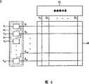
图4表示本发明的移位寄存器。移位寄存器4具有多个前后级相连的移位寄存单元,且受控于互为反相的时钟信号CK及XCK。本实施例以两移位寄存单元41至42为例,且移位寄存单元41的输出端OUT1连接移位寄存单元42的输入端IN2。每一移位寄存单元具有输入单元、输出单元、及控制单元。举例来说,移位寄存单元41具有输入单元U1、输出单元U2、及控制单元U3。Fig. 4 shows the shift register of the present invention. The
输入单元U1包括晶体管T46。输出单元U2包括晶体管T44及T45。控制单元包括晶体管T41至T43。The input unit U1 includes a transistor T46. The output unit U2 includes transistors T44 and T45. The control unit includes transistors T41 to T43.
在输入单元U1中,晶体管T46的栅极接收时钟信号XCK,且其漏极连接输入端IN1。In the input unit U1 , the gate of the transistor T46 receives the clock signal XCK, and the drain thereof is connected to the input terminal IN1 .
在输出单元U2中,晶体管T44的栅极连接晶体管T46的源极,其漏极连接时钟信号CK,且其源极连接输出端OUT1。晶体管T45的栅极连接控制单元U3的控制端CT,其漏极连接输出端OUT1,且其源极连接参考电源Vref。In the output unit U2 , the gate of the transistor T44 is connected to the source of the transistor T46 , the drain is connected to the clock signal CK, and the source is connected to the output terminal OUT1 . The gate of the transistor T45 is connected to the control terminal CT of the control unit U3 , its drain is connected to the output terminal OUT1 , and its source is connected to the reference power supply Vref.
在控制单元U3中,晶体管T41的栅极连接晶体管T46的源极,其漏极连接控制端CT,且其源极连接参考电源Vref。晶体管T42的栅极连接输出端OUT1,其漏极连接控制端CT,且其源极连接参考电源Vref。晶体管T43的栅极及漏极连接于电压源VDD,其源极连接控制端CT。其中,参考电源Vref为低电平,且电压源VDD为高电平。In the control unit U3, the gate of the transistor T41 is connected to the source of the transistor T46, its drain is connected to the control terminal CT, and its source is connected to the reference power supply Vref. The gate of the transistor T42 is connected to the output terminal OUT1 , the drain is connected to the control terminal CT, and the source is connected to the reference power supply Vref. The gate and drain of the transistor T43 are connected to the voltage source VDD, and the source of the transistor T43 is connected to the control terminal CT. Wherein, the reference power supply Vref is at a low level, and the voltage source VDD is at a high level.
图5表示本发明的移位寄存器的操作时序图。参阅第4及图5,且以移位寄存单元41至来举例说明。在期间P1中,输入信号IS1为高电平且时钟信号XCK为高电平。晶体管T46因此导通,且其源极输出高电平的第一信号FS。晶体管T41因其栅极接收第一信号FS而导通,使得控制端CT输出低电平的控制信号CS。晶体管T45因其栅极接收控制信号CS而关断。此外,晶体管T44的栅极接收第一信号FS。因此,晶体管T44导通,使得输出端OUT1输出低电平的输出信号OS1,以作为移位寄存单元41的输入信号IS2。FIG. 5 shows an operation timing chart of the shift register of the present invention. Referring to FIG. 4 and FIG. 5 , the
在接续的期间P2中,输入信号IS1变为低电平且时钟信号XCK变为低电平。晶体管T46关断,使得第一信号FS维持在高电平,更因为CK信号经由晶体管T44的寄生电容的耦合,使得第一信号FS提升至更高的电平。此时,晶体管T44导通且晶体管T45仍然关断,因此输出端OUT1输出高电平的输出信号OS1,以达到信号移位的作用。In the subsequent period P2, the input signal IS1 becomes low level and the clock signal XCK becomes low level. The transistor T46 is turned off, so that the first signal FS remains at a high level, and because the CK signal is coupled through the parasitic capacitance of the transistor T44 , the first signal FS is raised to a higher level. At this time, the transistor T44 is turned on and the transistor T45 is still turned off, so the output terminal OUT1 outputs a high-level output signal OS1 to achieve the function of signal shifting.
接着,在期间P3中,输入信号IS1维持在低电平且时钟信号XCK变为高电平。第一信号FS变为低电平,使得晶体管T41及T44关断。控制信号CS变成高电平,以导通晶体管T45,因此,输出端OUT1输出低电平的输出信号OS1。此时,由于晶体管T42因其栅极接收输出信号OS1而关断,因此控制信号CS可维持在高电平,使得晶体管T45持续导通,输出信号OS1则稳定地维持在低电平。Next, in the period P3, the input signal IS1 is maintained at a low level and the clock signal XCK is changed to a high level. The first signal FS becomes low level, so that the transistors T41 and T44 are turned off. The control signal CS becomes high level to turn on the transistor T45 , therefore, the output terminal OUT1 outputs a low level output signal OS1 . At this time, since the gate of the transistor T42 is turned off by receiving the output signal OS1 , the control signal CS can be maintained at a high level, so that the transistor T45 is continuously turned on, and the output signal OS1 is maintained at a stable low level.
在接下来的期间P4中,输入信号IS1持续维持在低电平且时钟信号XCK变低电平。由于晶体管T46关断,而无法确保第一信号FS维持在原来的低电平,使得晶体管44可能操作在次门限区而产生次门限电流,输出信号OS1因而无法稳定地维持在低电平。然而,由于本发明的晶体管T43为持续导通,因此,此时的控制信号CS则为高电平,以导通晶体管T45,使输出信号OS1更稳定地维持在低电平。此外,由于输出信号OS1更提供至晶体管T42的栅极,使得晶体管42关断,以确保控制信号CS维持在高电平。In the following period P4, the input signal IS1 is maintained at a low level and the clock signal XCK is turned to a low level. Since the transistor T46 is turned off, the first signal FS cannot be maintained at the original low level, so the transistor 44 may operate in the sub-threshold region to generate a sub-threshold current, and the output signal OS1 cannot be stably maintained at the low level. However, since the transistor T43 of the present invention is continuously turned on, the control signal CS at this time is at a high level to turn on the transistor T45 to keep the output signalOS1 at a low level more stably. In addition, since the output signal OS1 is further provided to the gate of the transistor T42 , the transistor 42 is turned off to ensure that the control signal CS remains at a high level.
综上所述,在移位寄存单元41中,根据时钟信号CK及XCK的控制,在输入单元U1接收高电平的输入信号IS1后,输出单元U2延迟输出高电平的输出信号OS1。控制单元U3则控制输出单元U2,使得当输入信号IS1维持在低电平且移位寄存单元41中非执行移位的操作时,输出信号OS1能稳定地维持在低电平。与常规技术比较起来,在本发明的移位寄存器中,每一级的移位寄存单元的输出信号可稳定,尤其是在执行完移位的操作且输入信号维持在低电平时,每一级的移位寄存单元的输出信号不会受到次门限电流的影响。To sum up, in the shift register unit41 , according to the control of the clock signals CK and XCK, after the input unit U1 receives the high-level input signalIS1 , the output unit U2 delays outputting the high-level output signal OS1 . The control unit U3 controls the output unit U2 so that when the input signal IS1 is maintained at a low level and the shift register unit41 is not performing a shift operation, the output signal OS1 can be stably maintained at a low level. Compared with the conventional technology, in the shift register of the present invention, the output signal of the shift register unit of each stage can be stable, especially when the shift operation is performed and the input signal is maintained at a low level, each stage The output signal of the shift register unit will not be affected by the sub-threshold current.
本发明的移位寄存器可应用于显示面板的数据驱动器或扫描驱动器,如图6中显示面板6的数据驱动器61或扫描驱动器62。以扫描驱动器62的移位寄存器63为例,移位寄存器63具有多个移位寄存单元61至6m,且每一移位寄存单元的结构与图4所示的结构相同。此外,每一级的移位寄存单元的输出信号不仅输入至下一级的移位寄存单元以作为其输入信号,也输入至对应扫描线S1至Sm。The shift register of the present invention can be applied to the data driver or the scan driver of the display panel, such as the
在本发明实施例中,以NMOS晶体管为例,实际上不以此为限。参考电源Vref可以接地线。此外,移位寄存器4以包括两个移位寄存单元为例,在实际利用上,移位寄存单元的数量可依据系统的需求而增加,且每一移位寄存单元具有输入端及输出端,In the embodiment of the present invention, an NMOS transistor is taken as an example, but it is not limited thereto. The reference power supply Vref may be grounded. In addition, the
综上所述,虽然本发明已以一较佳实施例公开如上,然其并非用以限定本发明,任何本领域技术人员,在不脱离本发明的精神和范围的情况下,可进行各种更动与修改,因此本发明的保护范围当视所提出的权利要求限定的范围为准。In summary, although the present invention has been disclosed as above with a preferred embodiment, it is not intended to limit the present invention. Any person skilled in the art can carry out various methods without departing from the spirit and scope of the present invention. Changes and modifications, therefore, the protection scope of the present invention should be determined by the scope defined by the proposed claims.
Claims (10)
Priority Applications (1)
| Application Number | Priority Date | Filing Date | Title |
|---|---|---|---|
| CNB2004100575556ACN100353460C (en) | 2004-08-16 | 2004-08-16 | Shift register and display panel using the shift register |
Applications Claiming Priority (1)
| Application Number | Priority Date | Filing Date | Title |
|---|---|---|---|
| CNB2004100575556ACN100353460C (en) | 2004-08-16 | 2004-08-16 | Shift register and display panel using the shift register |
Publications (2)
| Publication Number | Publication Date |
|---|---|
| CN1588555A CN1588555A (en) | 2005-03-02 |
| CN100353460Ctrue CN100353460C (en) | 2007-12-05 |
Family
ID=34603296
Family Applications (1)
| Application Number | Title | Priority Date | Filing Date |
|---|---|---|---|
| CNB2004100575556AExpired - Fee RelatedCN100353460C (en) | 2004-08-16 | 2004-08-16 | Shift register and display panel using the shift register |
Country Status (1)
| Country | Link |
|---|---|
| CN (1) | CN100353460C (en) |
Families Citing this family (18)
| Publication number | Priority date | Publication date | Assignee | Title |
|---|---|---|---|---|
| US7612770B2 (en)* | 2005-12-15 | 2009-11-03 | Tpo Displays Corp. | Systems for displaying images |
| CN100461254C (en)* | 2006-04-27 | 2009-02-11 | 友达光电股份有限公司 | Liquid crystal display and shift buffer unit thereof |
| EP1895545B1 (en)* | 2006-08-31 | 2014-04-23 | Semiconductor Energy Laboratory Co., Ltd. | Liquid crystal display device |
| JP4990034B2 (en)* | 2006-10-03 | 2012-08-01 | 三菱電機株式会社 | Shift register circuit and image display apparatus including the same |
| CN101206318B (en)* | 2006-12-22 | 2010-05-19 | 群康科技(深圳)有限公司 | Shifting register and LCD device |
| CN101211665B (en)* | 2006-12-29 | 2010-05-26 | 群康科技(深圳)有限公司 | Shift registers and LCD device |
| CN101241766B (en)* | 2007-02-09 | 2010-12-08 | 群康科技(深圳)有限公司 | Shift register and LCD device |
| CN101241247B (en)* | 2007-02-09 | 2010-05-26 | 群康科技(深圳)有限公司 | Shift registers and LCD device |
| CN101339810B (en)* | 2007-07-06 | 2010-08-25 | 群康科技(深圳)有限公司 | Shift register and LCD device using the same |
| TWI410944B (en) | 2009-06-10 | 2013-10-01 | Au Optronics Corp | Shift register of a display device |
| CN101609719B (en)* | 2009-07-22 | 2011-12-28 | 友达光电股份有限公司 | Shift register of display device |
| CN102509537B (en)* | 2009-07-22 | 2013-07-10 | 友达光电股份有限公司 | Shift register of display device |
| TWI424789B (en)* | 2010-11-11 | 2014-01-21 | Au Optronics Corp | Gate driving circuit on lcd panel |
| CN102169669B (en)* | 2011-04-28 | 2013-04-10 | 北京大学深圳研究生院 | Grid drive circuit unit and grid drive circuit |
| TWI443627B (en)* | 2012-06-14 | 2014-07-01 | Au Optronics Corp | Scan driving apparatus and driving signal generating method thereof |
| CN103295642B (en)* | 2012-09-19 | 2016-02-17 | 上海中航光电子有限公司 | Shift register and panel display apparatus |
| CN112534494B (en)* | 2019-07-02 | 2023-12-12 | 京东方科技集团股份有限公司 | Shift register unit, driving method and device thereof |
| CN113823640B (en) | 2020-05-11 | 2024-10-18 | 京东方科技集团股份有限公司 | Display substrate and display device |
Citations (4)
| Publication number | Priority date | Publication date | Assignee | Title |
|---|---|---|---|---|
| US4084106A (en)* | 1975-12-17 | 1978-04-11 | Itt Industries, Incorporated | Dynamic shift register using insulated-gate field-effect transistors |
| CN1298169A (en)* | 1999-11-01 | 2001-06-06 | 夏普公司 | Shift register and image display device |
| US6345085B1 (en)* | 1999-11-05 | 2002-02-05 | Lg. Philips Lcd Co., Ltd. | Shift register |
| CN1395256A (en)* | 2001-06-29 | 2003-02-05 | 卡西欧计算机株式会社 | Shift register and electronic device |
- 2004
- 2004-08-16CNCNB2004100575556Apatent/CN100353460C/ennot_activeExpired - Fee Related
Patent Citations (4)
| Publication number | Priority date | Publication date | Assignee | Title |
|---|---|---|---|---|
| US4084106A (en)* | 1975-12-17 | 1978-04-11 | Itt Industries, Incorporated | Dynamic shift register using insulated-gate field-effect transistors |
| CN1298169A (en)* | 1999-11-01 | 2001-06-06 | 夏普公司 | Shift register and image display device |
| US6345085B1 (en)* | 1999-11-05 | 2002-02-05 | Lg. Philips Lcd Co., Ltd. | Shift register |
| CN1395256A (en)* | 2001-06-29 | 2003-02-05 | 卡西欧计算机株式会社 | Shift register and electronic device |
Also Published As
| Publication number | Publication date |
|---|---|
| CN1588555A (en) | 2005-03-02 |
Similar Documents
| Publication | Publication Date | Title |
|---|---|---|
| CN100353460C (en) | Shift register and display panel using the shift register | |
| KR101710661B1 (en) | Gate driving circuit and display apparatus having the same | |
| US9607565B2 (en) | Display device and method of initializing gate shift register of the same | |
| JP4854929B2 (en) | Shift register and display device having the same | |
| US7817771B2 (en) | Shift register | |
| TWI331339B (en) | Shift register circuit and display drive device | |
| JP5127986B2 (en) | Shift register, scanning signal line drive circuit and display device having the same | |
| JP4480944B2 (en) | Shift register and display device using the same | |
| JP2002313093A (en) | Shift register, drive circuit, electrode substrate, and flat panel display | |
| JP2008020675A (en) | Image display device | |
| JP2001159877A (en) | Matrix type image display device | |
| JP2009049985A (en) | Method for reducing bootstrap point voltage of electronic circuit and apparatus using the method | |
| CN113823236B (en) | Shift register and display device | |
| KR20070080440A (en) | Display substrate and display device having same | |
| US20080158133A1 (en) | Shift register and liquid crystal display device using same | |
| US7505022B2 (en) | Shift register and display device | |
| JP2009181612A (en) | Shift register circuit and liquid crystal display unit | |
| KR20080041458A (en) | Internal Clock Generation Circuit and Data Driver Using It | |
| JPH09182004A (en) | Scanning circuit and image display device | |
| JPH08248926A (en) | Active matrix liquid crystal display device and driving method thereof | |
| KR20070074841A (en) | Liquid crystal display | |
| CN113168880A (en) | GOA unit and its GOA circuit, display device | |
| CN101894540B (en) | Driving signal generating circuit and signal generating method thereof | |
| JP3856316B2 (en) | Shift register circuit and image display device | |
| CN113160732B (en) | Gate drive circuit |
Legal Events
| Date | Code | Title | Description |
|---|---|---|---|
| C06 | Publication | ||
| PB01 | Publication | ||
| C10 | Entry into substantive examination | ||
| SE01 | Entry into force of request for substantive examination | ||
| C14 | Grant of patent or utility model | ||
| GR01 | Patent grant | ||
| CF01 | Termination of patent right due to non-payment of annual fee | Granted publication date:20071205 | |
| CF01 | Termination of patent right due to non-payment of annual fee |