CN100353288C - Device for processing data and method for processing data - Google Patents
Device for processing data and method for processing dataDownload PDFInfo
- Publication number
- CN100353288C CN100353288CCNB2003801087534ACN200380108753ACN100353288CCN 100353288 CCN100353288 CCN 100353288CCN B2003801087534 ACNB2003801087534 ACN B2003801087534ACN 200380108753 ACN200380108753 ACN 200380108753ACN 100353288 CCN100353288 CCN 100353288C
- Authority
- CN
- China
- Prior art keywords
- data processing
- performance
- level
- processor
- clock
- Prior art date
- Legal status (The legal status is an assumption and is not a legal conclusion. Google has not performed a legal analysis and makes no representation as to the accuracy of the status listed.)
- Expired - Lifetime
Links
Images


Classifications
- G—PHYSICS
- G06—COMPUTING OR CALCULATING; COUNTING
- G06F—ELECTRIC DIGITAL DATA PROCESSING
- G06F1/00—Details not covered by groups G06F3/00 - G06F13/00 and G06F21/00
- G06F1/26—Power supply means, e.g. regulation thereof
- G06F1/32—Means for saving power
- G06F1/3203—Power management, i.e. event-based initiation of a power-saving mode
- G06F1/3234—Power saving characterised by the action undertaken
- G06F1/3237—Power saving characterised by the action undertaken by disabling clock generation or distribution
- G—PHYSICS
- G06—COMPUTING OR CALCULATING; COUNTING
- G06F—ELECTRIC DIGITAL DATA PROCESSING
- G06F1/00—Details not covered by groups G06F3/00 - G06F13/00 and G06F21/00
- G06F1/26—Power supply means, e.g. regulation thereof
- G06F1/32—Means for saving power
- G06F1/3203—Power management, i.e. event-based initiation of a power-saving mode
- G06F1/3234—Power saving characterised by the action undertaken
- G06F1/324—Power saving characterised by the action undertaken by lowering clock frequency
- G—PHYSICS
- G06—COMPUTING OR CALCULATING; COUNTING
- G06F—ELECTRIC DIGITAL DATA PROCESSING
- G06F1/00—Details not covered by groups G06F3/00 - G06F13/00 and G06F21/00
- G06F1/26—Power supply means, e.g. regulation thereof
- G06F1/32—Means for saving power
- G06F1/3203—Power management, i.e. event-based initiation of a power-saving mode
- G06F1/3234—Power saving characterised by the action undertaken
- G06F1/3296—Power saving characterised by the action undertaken by lowering the supply or operating voltage
- Y—GENERAL TAGGING OF NEW TECHNOLOGICAL DEVELOPMENTS; GENERAL TAGGING OF CROSS-SECTIONAL TECHNOLOGIES SPANNING OVER SEVERAL SECTIONS OF THE IPC; TECHNICAL SUBJECTS COVERED BY FORMER USPC CROSS-REFERENCE ART COLLECTIONS [XRACs] AND DIGESTS
- Y02—TECHNOLOGIES OR APPLICATIONS FOR MITIGATION OR ADAPTATION AGAINST CLIMATE CHANGE
- Y02D—CLIMATE CHANGE MITIGATION TECHNOLOGIES IN INFORMATION AND COMMUNICATION TECHNOLOGIES [ICT], I.E. INFORMATION AND COMMUNICATION TECHNOLOGIES AIMING AT THE REDUCTION OF THEIR OWN ENERGY USE
- Y02D10/00—Energy efficient computing, e.g. low power processors, power management or thermal management
Landscapes
- Engineering & Computer Science (AREA)
- Theoretical Computer Science (AREA)
- Physics & Mathematics (AREA)
- General Engineering & Computer Science (AREA)
- General Physics & Mathematics (AREA)
- Power Sources (AREA)
- Executing Machine-Instructions (AREA)
- Microcomputers (AREA)
Abstract
Description
Translated fromChinese技术领域technical field
本发明涉及数据处理系统领域。更特别地是,本发明涉及控制数据处理性能诸如以减少由数据处理系统消耗的能量的领域。The present invention relates to the field of data processing systems. More particularly, the present invention relates to the field of controlling data processing performance such as to reduce the energy consumed by a data processing system.
背景技术Background technique
在数据处理系统中重要考虑因素是它们的能量消耗。消耗较少能量的数据处理系统在移动设备中允许更长的电池寿命,易于较冷并可靠地运行,并且对于处理热损耗等,要求较少的专用设计考虑因素。非常希望减少数据处理系统的能量消耗。An important consideration in data processing systems is their energy consumption. A data processing system that consumes less energy allows for longer battery life in mobile devices, tends to run cooler and more reliably, and requires fewer dedicated design considerations to deal with heat loss, among others. It is highly desirable to reduce the energy consumption of data processing systems.
与希望减少数据处理系统的能量消耗相平衡的是同时希望提高它们的性能级别,以便处理日益计算集中的任务。这种任务短时间内常常要求非常集中的处理操作,在所述短时间后面是其中要求少量计算的相对长的空闲时间。Balanced with the desire to reduce the energy consumption of data processing systems is the simultaneous desire to increase their performance levels in order to handle increasingly computationally intensive tasks. Such tasks often require very intensive processing operations for a short period of time followed by relatively long idle periods in which few calculations are required.
为了解决上述两个因素,已知提出这样的数据处理系统,其能改变它们的性能级别以便在某些配置中提供高计算性能而在其它配置中提供低能量消耗。诸如由Transmeta生产的LongRun软件或由Intel生产的SpeedStep系统之类的已知系统,使处理器能够在这种不同的配置之间切换。为了匹配想要的性能目标,高计算性能配置往往是这样的配置,具有相对高的操作电压和相对高的处理器时钟频率。反之,低能量消耗配置具有相对低的操作电压和相对低的处理器时钟频率。In order to address the above two factors, it is known to propose data processing systems that can vary their performance levels in order to provide high computing performance in certain configurations and low energy consumption in other configurations. Known systems, such as the LongRun software produced by Transmeta or the SpeedStep system produced by Intel, enable the processor to switch between such different configurations. To match desired performance goals, high computing performance configurations are often configurations that have relatively high operating voltages and relatively high processor clock frequencies. Conversely, a low power consumption configuration has a relatively low operating voltage and a relatively low processor clock frequency.
EP-A-0,632,360公开了一种根据功率选择信号可在电压和频率级别之间切换的计算机系统。所想要的操作功率可以根据空闲时间来迭代确定。EP-A-0,632,360 discloses a computer system switchable between voltage and frequency levels according to a power selection signal. The desired operating power can be determined iteratively based on idle time.
US-A-5,627,412公开了一种响应于对操作功率的波动需求而可以动态切换的电源。US-A-5,627,412 discloses a power supply that can be dynamically switched in response to fluctuating demands on operating power.
除提供上述性能和能量管理能力之外,另一重要的设计特性是硬件和软件设计在相对较多的不同环境中应该是可以重新使用的。如果对于不同的硬件实现必须重新编写诸如操作系统软件之类的计算机软件,或者对于不同的硬件实现要较大地修改硬件设计,那么这是非常不利的。In addition to providing the performance and energy management capabilities described above, another important design characteristic is that the hardware and software design should be reusable in a relatively large number of different environments. This is very disadvantageous if computer software, such as operating system software, has to be rewritten for a different hardware implementation, or if the hardware design is to be substantially modified for a different hardware implementation.
发明内容Contents of the invention
依照一个方面,本发明提供了一种用于处理数据的设备,所述设备包括:According to one aspect, the present invention provides an apparatus for processing data, the apparatus comprising:
处理器,可操作来执行数据处理操作,所述处理器可操作来产生性能控制信号,所述性能控制信号表示想要的、所述处理器的数据处理性能级别;和a processor operable to perform data processing operations, the processor operable to generate a performance control signal indicative of a desired data processing performance level of the processor; and
至少一个另外的电路,响应于所述性能控制信号操作来支持所述想要的、所述处理器的数据处理性能级别;其中at least one additional circuit operative to support said desired data processing performance level of said processor in response to said performance control signal; wherein
当响应对应于从第一想要的数据处理性能级别到第二想要的数据处理性能级别变化的、性能控制信号的变化时,所述至少一个另外的电路可操作来在至少一个中间数据处理性能级别支持数据处理,并且所述处理器在所述变化期间暂时在所述至少一个中间数据处理性能级别操作。Said at least one further circuit is operable to switch between at least one intermediate data processing performance level in response to a change in the performance control signal corresponding to a change from a first desired data processing performance level to a second desired data processing performance level. A performance level supports data processing, and said processor temporarily operates at said at least one intermediate data processing performance level during said change.
本技术提供了一种系统,其中当响应性能控制信号的变化时,所述另外的电路可操作来支持至少一个中间数据处理性能级别,并且所述处理器利用其来在所述变化期间在所述至少一个中间数据处理性能级别上操作。一旦较高中间性能级别可用来在执行所关注的代码过程中有助于更好的向前进展,正在发生的性能变化就可以是随采用的所述较高中间性能级别的增高而在性能级别上的提高。作为选择,在性能级别下降期间,一旦较低中间性能级别可用来更迅速地减少能量消耗,这种技术就导致所述较低中间性能级别被采用。The present technique provides a system wherein said additional circuitry is operable to support at least one intermediate data processing performance level when responsive to a change in a performance control signal, and wherein said processor utilizes the same to operate at said level during said change. operating at at least one of the intermediate data processing performance levels. Once a higher intermediate performance level is available to facilitate better forward progress in the execution of the code of interest, the performance change that is taking place may be a decrease in performance level as the higher intermediate performance level is employed on the improvement. Alternatively, during a drop in performance level, this technique results in a lower intermediate performance level being employed once the lower intermediate performance level becomes available to reduce energy consumption more rapidly.
在性能级别提高的情况下,可以在到达那个提高的性能级别之前删除对于提高的性能级别的要求。作为一个例子,当服务高优先级但是相对计算不集中时,中断可以触发试图切换到最大性能级别,但是事实上只在几个处理周期内就完全地执行了中断代码,并且在该处理级别上升至最大量之前很早就完全地执行了中断代码,中间处理级的使用更迅速地启用该中断服务。当消除了对较高处理级的需要时,设置新的想要的数据处理性能级别,取消切换到最大性能级别。In the case of an increased performance level, the requirement for the increased performance level may be removed prior to reaching that increased performance level. As an example, when a service is high priority but relatively computationally intensified, an interrupt can trigger an attempt to switch to the maximum performance level, but in fact only executes the interrupt code completely within a few processing cycles, and at that processing level goes up The use of intermediate processing stages enables the interrupt servicing much more quickly before the interrupt code is fully executed long before the maximum. When the need for a higher processing level is eliminated, a new desired data processing performance level is set, canceling switching to the maximum performance level.
尽管当前技术适用于控制多种不同类型的其它电路,但是当控制时钟发生器和电压控制器时其尤为有用。在这种环境中,一旦更高的频率可用并且电源电压足以支持该提高速度的操作时,可以切换到该更高的时钟频率以便更好地向前进展通过所关注的程序代码,即使该更高的时钟频率可能只是一个接近于想要的最终目标频率的中间频率也是如此。While the current technology is applicable to controlling many different types of other circuits, it is particularly useful when controlling clock generators and voltage controllers. In this environment, once the higher frequency is available and the supply voltage is sufficient to support the increased speed operation, it is possible to switch to the higher clock frequency to better progress forward through the program code in question, even if the higher frequency It's also true that the high clock frequency may only be an intermediate frequency close to the desired final target frequency.
本发明的优选实施例还提供了优先级信号,其能够触发改变到预先确定的性能级别,而不管控制信号值(例如最大或降低的级别)。这允许硬件机制采用可以便于迅速响应环境的方式来直接控制性能级别,所述环境诸如硬件中断、降低的电池功率信号等。A preferred embodiment of the present invention also provides a priority signal that can trigger a change to a predetermined performance level regardless of the control signal value (eg maximum or reduced level). This allows hardware mechanisms to directly control performance levels in a manner that can facilitate rapid response to circumstances, such as hardware interrupts, reduced battery power signals, and the like.
从另一方面观察,本发明提供了处理数据的方法,所述方法包括步骤:Viewed from another aspect, the invention provides a method of processing data, said method comprising the steps of:
用处理器来执行数据处理操作,所述处理器可操作来产生性能控制信号,所述性能控制信号表示所述想要的、所述处理器的数据处理性能级别;并且performing data processing operations with a processor operable to generate a performance control signal indicative of said desired data processing performance level of said processor; and
响应于所述性能控制信号,操作一个或多个另外的电路以便支持所述想要的、所述处理器的数据处理性能级别;其中operating one or more additional circuits to support said desired data processing performance level of said processor in response to said performance control signal; wherein
当响应对应于从第一想要的数据处理性能级别到第二想要的数据处理性能级别变化的、性能控制信号的变化时,所述一个或多个另外的电路可操作来在至少一个中间数据处理性能级别支持数据处理,并且所述处理器在所述变化期间暂时在所述至少一个中间数据处理性能级别操作。The one or more additional circuits are operable to switch between at least one intermediate A data processing performance level supports data processing, and said processor temporarily operates at said at least one intermediate data processing performance level during said change.
附图说明Description of drawings
现在将仅以举例形式,参考附图来描述本发明的实施例,其中:Embodiments of the invention will now be described, by way of example only, with reference to the accompanying drawings, in which:
图1示意地举例说明了数据处理系统的一部分,包括性能控制器、时钟发生器和电压控制器;Figure 1 schematically illustrates a part of a data processing system, including a performance controller, a clock generator and a voltage controller;
图2是示意地举例说明了在设置想要的性能级别过程中操作系统计算机程序操作的流程图;Figure 2 is a flowchart schematically illustrating the operation of an operating system computer program in setting a desired performance level;
图3示意地举例说明了在想要的性能级别和控制信号值之间的示例性映射;Figure 3 schematically illustrates an exemplary mapping between desired performance levels and control signal values;
图4是示意地举例说明了控制电压控制器的流程图;Figure 4 is a flow diagram schematically illustrating a control voltage controller;
图5是示意地举例说明了控制时钟发生器的流程图;Figure 5 is a flow diagram schematically illustrating a control clock generator;
图6是示意地举例说明了利用当前技术的数据处理系统的另一例子的图;Figure 6 is a diagram schematically illustrating another example of a data processing system utilizing the current technology;
图7是示意地举例说明了在想要性能级别和控制信号值之间映射的进一步例子的图;Figure 7 is a diagram schematically illustrating a further example of mapping between desired performance levels and control signal values;
图8举例说明了电源电压在保持模式级别和处理模式级别之间的调制;Figure 8 illustrates the modulation of supply voltage between hold mode level and process mode level;
图9示意地举例说明了结合图8技术的电路;Figure 9 schematically illustrates a circuit incorporating the technique of Figure 8;
图10是示意地举例说明了使用调制的电压来控制性能的流程图;Figure 10 is a flowchart schematically illustrating the use of modulated voltages to control performance;
图11是示意地举例说明使用图8技术的另一数据处理系统的图;和Figure 11 is a diagram schematically illustrating another data processing system using the technique of Figure 8; and
图12是举例说明用于诸如图8到11的实施例的各个控制信号的图。FIG. 12 is a diagram illustrating various control signals for embodiments such as FIGS. 8-11.
具体实施方式Detailed ways
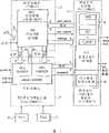
图1举例说明了数据处理系统的一部分,包括性能控制器2、时钟发生器4和电压控制器6。典型地是,在图1中的电路形成较大集成电路的一部分,所述集成电路包括处理器,诸如由英国剑桥ARM有限公司生产的ARM处理器,以及其它电路元件,也可以作为芯片内系统设计的一部分。为了简化起见,从图1中省略了除性能控制器2、时钟发生器4和电压控制器6之外的电路元件。所述性能控制器2接收性能级别请求信号/值,该信号/值由在处理器(未举例说明)上执行的计算机程序在程序指令的控制下产生,所述计算机程序诸如操作计算机程序。为了该目的,可以把所想要的数据处理性能级别请求写入在存储地址空间内专用存储单元上,也可以写入到控制寄存器(诸如在例如CP5 ARM体系结构之类的配置协处理器内的控制寄存器),或者采用其它方式存储。性能控制器2还结合性能监视器,所述性能监视器可以是一个或多个性能计数器,其计数实际时间、时钟信号、执行的工作或其它性能监视参数的经过。当性能控制器2接收表示想要的性能级别上的变化的数据处理性能级别请求时,那么其用来向时钟发生器4发布对新的目标时钟速度的请求以及向电压控制器6发布对新的目标电压的请求。应当理解的是,一旦程序指令将其想要的数据处理性能级别写入到适当的位置时,它就把控制如何实施所述想要的数据处理性能级别的控制权交给硬件(性能控制器2)。所述性能控制器2把所想要的数据处理性能请求映射到对时钟发生器4和电压控制器6适当的控制信号值(所述性能控制器2包括映射电路)。数据处理性能请求信号可以是格雷(Gray)编码信号值或简单的线性编码值。所述映射可以是温度计编码控制信号值,因为这样就对在可能是异步的时钟域之间采样时针对采样错误提供较好的抵抗性。此外,这提供了一种故障安全状态,借此采样错误易于生成最低的稳定同步值以供使用。FIG. 1 illustrates a portion of a data processing system including a
传送到电压控制器6的控制信号命令所述电压控制器6采纳新的电压输出电平。可以通过在引导或其它时间编程在电压控制器6内配置参数寄存器8来配置所支持的电压输出电平。电压控制器6花费有限时间量来上升或下降至新的电压电平。在一些实施例中,当电压控制器6正在改变到其新的电压电平时,所述电压控制器6可以穿过一个或多个中间级别,所述中间级别往往能够支持挂起正在到达的最后性能级别的一个中间性能级别(在稍后描述的其它实施例中,可以使用单个的操作频率时钟信号和停止时钟)。电压控制器6产生表示其可以支持的当前电压电平的当前操作信号并且把这些信号传回到性能控制器2,此处这些信号可以按照如下来动作,即用于触发对适当且可用的相关联时钟频率的使用。A control signal to the
性能控制器2还把由程序控制指定的、所想要的数据处理性能级别转换为被传送到时钟发生器4的控制信号。这些控制信号指定目标时钟频率。向时钟发生器4提供来自一个或多个锁相环电路10、12的各种时钟信号。这些锁相环电路之一10是永久启用的,并且用来提供可支持的最小和最大时钟频率以及一些中间频率。另一锁相环电路12是选择性地可用的,并且当不要求其产生中间时钟频率时可以断电以便节能。The
时钟发生器4产生性能控制器时钟信号,将其提供给在所述电压控制器6内的技术相关松弛检测器(technology dependent slackdetector)14。这种安排可用于在电压控制器6内提供附加的控制级别,使得该电压控制器6正在产生的电压可以调节成支持目标时钟频率并具有降低的过冲,即所产生的电压电平刚好足以支持所述目标时钟频率,并带有小的缓冲器。可以把所述电压输出的精细控制级别认为是对响应于由程序指令指定的、所想要的数据处理性能级别改变而实施的粗略性能级别的辅助。当已经表明改变到提高的性能级别时,电压控制器6将试图提高其正在产生的电压,并且当其提供提高的电压时,向性能控制器2返回表明这一情况,所述性能控制器2依次可以控制在时钟发生器4内的CPU时钟发生器来输出CPU时钟信号cpuclk,以便向具有可支持的新时钟频率的处理器提供新的电压,所述频率可以是接近于所最终想要的时钟频率的中间时钟频率。时钟发生器4可能不能产生具有可以在控制信号值中指定粒度的时钟信号,并且相应地传回对应于其正在产生的实际时钟频率的量化时钟信号值。作为选择,这种考虑所述时钟发生器4实际能力的量化能够在由性能控制器所执行的、从所想要的数据处理性能请求到控制信号的映射之内发生。在稍后论述的另一实施例中,电压控制器具有两个可能的电压输出电平,高电平供处理模式使用,而低电平供在停止时钟时保持模式使用。A
图2示意地举例说明了依照所述技术一个例子的处理操作,其可以由在处理器上执行的操作系统计算机程序来执行。在步骤16,相关处理线程等待着,直到确定需要改变性能级别。这一需要可以由外部参数变化来表明,诸如由用户按压键,或可以使用诸如先前论述的那些性能监视计数器通过监视所述系统的运算性能来在内部触发。当检测到这种想要的性能级别变化时,处理继续至步骤18,在此所述软件执行写入存储器映射的单元,所述单元专用于存储所想要的数据处理性能的请求级别。计算机程序代码的动作将检测对改变性能级别的要求并且把该要求写入存储单元。不需要向监视器提供控制反馈:所想要的性能改变实际上发生或其怎样发生。在计算机程序进行写入的动作和按照请求而动作的基础硬件机制之间存在抽象。这使在各种环境中使用基本上不变的计算机程序便于进行,在那些环境内可以或可以不提供任何性能管理机制。Figure 2 schematically illustrates processing operations according to one example of the described technology, which may be performed by an operating system computer program executing on a processor. At
图3示意地举例说明了在6位想要的数据处理性能请求信号(其可选地是格雷码)和对应的温度计编码控制信号值之间的示例性映射。在这种情况下,尽管存在33个可能的性能级别,但是却只存在9个可能的控制信号值。相应地,在所想要的性能级别和控制信号值之间存在量化。该量化被安排成使得所述控制信号值对应于在性能级别范围内且可以被映射到该控制信号值的最大性能级别。在想要的性能信号和意在指定的性能级别中存在单调递增。从而,所想要的性能级别可以是表示在系统中可实现的最大性能级别百分比的二进制小数。这是方便而又灵活的、抽象所述性能级别请求的途径,用来抽象所述性能级别请求的方式是:所述性能级别请求可以在多种不同的硬件环境中并且为多种不同的处理目而由程序指令加以控制。Figure 3 schematically illustrates an exemplary mapping between a 6-bit desired data processing performance request signal (which is optionally Gray coded) and a corresponding thermometer encoded control signal value. In this case, although there are 33 possible performance levels, there are only 9 possible control signal values. Accordingly, there is a quantification between the desired performance level and the control signal value. The quantization is arranged such that the control signal value corresponds to the maximum performance level within the range of performance levels that can be mapped to the control signal value. There is monotonically increasing in the desired performance signal and the intended performance level. Thus, the desired performance level may be a binary fraction representing a percentage of the maximum performance level achievable in the system. This is a convenient and flexible way of abstracting the performance level request in such a way that the performance level request can be processed in a variety of different hardware environments and for a variety of different The purpose is controlled by program instructions.
图4示意地举例说明了在具有多个电压电平的实施例中电压控制器6的控制,所述电压电平对应于其中时钟正在运行的活动处理模式。在步骤20,所述电压控制器等待接收新的控制信号。当接收新的控制信号时,处理继续至步骤22,在此启动所提供的电压电平的改变。该改变可以是提高或降低。电压控制器6具有能够改变它的输出的有限转换率(slew rate)。步骤24监视着,直到在发生总变化期间到达下一可支持的电压电平为止。当到达这种下一级别时,那么启动步骤26并且产生新的当前电压输出信号,以便向回提供给性能控制器2以表明所述电压控制器6能够支持所述新的电压电平。这可以是接近于最终目标电压电平的中间电压电平,或者在所述转换(slew)末尾是最终目标电压电平本身。所述性能控制器2可以按照反馈到它的当前电压输出信号来动作,以便控制时钟发生器以及可能的性能监视电路。步骤28确定是否已经达到最终电压。如果还没有达到所述最终电压,那么处理回到步骤24并且电压输出的转换继续朝向其最终目标。在只支持两个电压电平的系统中,所述系统将在没有中间电压电平的情况下会简单地等待着达到最终电压电平。Figure 4 schematically illustrates the control of the
应当理解的是,图4假定控制信号不改变。实际上,所述控制信号可以在到达最终目标电压之前改变。对由在操作系统内程序指令所确定的性能级别临时改变的需要可能已经不复存在,诸如中断已经得到服务或者应急模式信号已经被置为无效。在这种环境中,中断在图4中举例说明的控制,并且处理回到步骤20,在那里启动基于新建立的控制信号值的动作。应当理解的是,由软件所进行的控制至少是部分开环的,这是由于该控制仅仅规定了其在特定时间点上所想要的性能级别,而并不要求监视实际上递送的性能,或实际上何时递送所述性能级别。It should be understood that Figure 4 assumes that the control signal does not change. In fact, the control signal can be changed before reaching the final target voltage. The need for a temporary change in performance level as determined by program instructions within the operating system may no longer exist, such as if an interrupt has been serviced or a panic mode signal has been deasserted. In such circumstances, the control illustrated in FIG. 4 is interrupted, and processing returns to step 20, where an action based on the newly established control signal value is initiated. It should be understood that control by software is at least partially open loop in that the control only specifies the level of performance it desires at a particular point in time and does not require monitoring of the performance actually delivered, Or when that performance level is actually delivered.
如所提及,可以把应急信号(优先级信号或硬件重载信号)提供给性能控制器2以便重载性能级别的任何软件控制并且暂时把所述性能级别提高到最大级别。旁路性能级别的软件控制可以便于在纯粹的硬件控制下更迅速且直接地切换到最大性能级别,诸如响应于特定的高优先级硬件中断信号来进行所述切换。可以提供不止一个这种“应急”信号,例如“低电池应急”信号可以把性能强迫到已知降低的级别。As mentioned, an emergency signal (either a priority signal or a hardware reload signal) may be provided to the
图5示意地举例说明了时钟发生器4的控制。在步骤30,所述时钟发生器等待接收新的控制信号。当接收到新的控制信号时,处理继续至步骤32,在那里确定是否需要给任何附加锁相环电路12加电以便服务最终要求的新时钟频率。如果要求这种附加锁相环电路12,那么处理继续至步骤34,在那里启动所述附加锁相环电路12。作为选择,处理直接进行至步骤36。FIG. 5 schematically illustrates the control of the
在步骤36,所述时钟发生器确定接近于所请求性能级别的新的时钟信号是否可用。这便于采用用于挂起最终目标性能级别可用性的中间性能级别。当识别这种中间时钟频率时,那么处理继续至步骤38。步骤38确定从电压控制器6反馈的当前操作信号值是否表明正在产生能够支持新的时钟信号值的电压。当这种电压可用时,那么处理继续至步骤40,在那里由CPU时钟发生器采用并产生新的时钟信号值以作为信号cpuclk,所述信号cpuclk被提供给处理器核心。然后,步骤42反向给性能控制器2输出新的当前时钟值,此处所述性能监视硬件可以遵照所述新的当前时钟值来动作以便估计向前通过代码的进展。步骤44确定:到新的时钟频率的切换,是否已经是到已由程序指令产生的、想要数据处理性能请求所指定的最终时钟频率的切换。如果没有达到最终目标时钟频率,那么处理回到步骤36,否则控制终止(实际上回到步骤30)。At
至于图4,图5也假定不改变由程序指令所指定的想要的数据处理性能级别。如果所述想要的数据处理性能级别改变,那么将要产生新的映射控制信号值,所述控制信号值中断在图5中举例说明的处理并且使所述处理返回到步骤30,于是照新的控制信号值动作。As with Figure 4, Figure 5 also assumes no change to the desired data processing performance level specified by the program instructions. If the desired data processing performance level changes, a new mapping control signal value will be generated that interrupts the process illustrated in FIG. 5 and returns the process to step 30, whereupon the new Controls the signal value action.
当在初始和最终时钟频率值之间改变时采用中间时钟频率值,对于所关注电路的特定状态而言,允许最好的通过代码向前进展得以实现。在最终目标时钟频率变得可用之前,所述电路一直都不在初始时钟频率操作,而是相反,当在性能转换期间每个时钟频率变得可用时,所述电路上升或下降穿过时钟频率序列。可以把采用新的时钟频率认为是由如下信号的逻辑与(AND)来控制的,所述信号包括:用于表明所述频率比当前频率更接近目标频率的信号、用于表明来自时钟源的那个频率可用性的信号、以及用于表明电压控制器能够生成具有足以支持该新时钟频率的操作的功率信号的信号。作为选择,在只具有两个性能级别(最大/空闲)的其它实施例中,所述系统在进行切换之前会等待最终电压。Employing intermediate clock frequency values when changing between initial and final clock frequency values allows the best forward progress through the code to be achieved for a particular state of the circuit of interest. The circuit does not operate at the initial clock frequency until the final target clock frequency becomes available, but instead the circuit ramps up or down through the sequence of clock frequencies as each clock frequency becomes available during a performance transition . The adoption of a new clock frequency can be considered to be controlled by the logical AND (AND) of the following signals: a signal indicating that the frequency is closer to the target frequency than the current frequency, a signal indicating that the frequency from the clock source A signal of that frequency availability, and a signal indicating that the voltage controller is capable of generating a power signal sufficient to support operation at the new clock frequency. Alternatively, in other embodiments with only two performance levels (max/idle), the system waits for the final voltage before switching.
图6是示意地举例说明利用当前技术的数据处理系统的图。与在图1中举例说明的相同的元件具有相同的附图标记。图6另外举例说明了执行程序指令的处理器46,所述程序指令可以保持在紧耦合的存储器系统48或其它存储器内。所关注的不同电压范围使在举例说明的电路中的各个接口处提供电平移动器(shifter)很有必要。Figure 6 is a diagram schematically illustrating a data processing system utilizing the current technology. The same elements as illustrated in FIG. 1 have the same reference numerals. FIG. 6 additionally illustrates a processor 46 executing program instructions, which may be maintained in a tightly coupled memory system 48 or other memory. The different voltage ranges of interest necessitate the provision of level shifters at the various interfaces in the illustrated circuits.
图7举例说明了在想要的数据处理性能请求级别和温度计编码控制信号值之间的另一示例性映射。在这一情况下,使用32位温度计编码控制信号值,产生更细度的性能控制的可能性。响应于这32位控制信号值的另外电路可能只能够提供更粗粒度的控制,因此实际上在内部量化所关注的控制信号值。温度计编码控制信号值提供了特别便利的方式来组合来自不同源的控制信号值,诸如来自多处理器系统上的不同的处理器的控制信号值,借此可以适当选择总体性能级别,其只在芯片范围的基础上可能才是可控制的。可以用控制信号值的逻辑或(OR)来确定最大控制信号值,可以用控制信号值的逻辑与(AND)来确定最小控制信号值,并且可以用控制信号值的异或XOR来确定等效值。最大值函数可以用于确定最大请求的时钟频率,最小值函数可以用于表明最小可支持的电压,而等效函数可以用于确定在不同元件需求之间的匹配。FIG. 7 illustrates another exemplary mapping between desired data processing performance request levels and thermometer encoded control signal values. In this case, a 32-bit thermometer is used to encode the control signal value, yielding the possibility of finer-grained performance control. Additional circuitry responsive to these 32-bit control signal values may only be able to provide a coarser grained control, thus actually internally quantizing the control signal value of interest. Thermometer-encoded control signal values provide a particularly convenient way to combine control signal values from different sources, such as from different processors on a multiprocessor system, whereby the overall performance level can be appropriately chosen, which is only available in It may only be controllable on a chip-wide basis. The logical OR (OR) of the control signal values can be used to determine the maximum control signal value, the logical AND (AND) of the control signal values can be used to determine the minimum control signal value, and the exclusive OR (XOR) of the control signal values can be used to determine the equivalent value. The maximum function can be used to determine the maximum requested clock frequency, the minimum function can be used to indicate the minimum supportable voltage, and the equivalence function can be used to determine the match between different component requirements.
图8举例说明了另一性能控制技术。在该例子中,把对处理电路的电源电压示为是在保持模式电压电平HM和处理模式电压电平PM之间调制的(在该例子中为脉冲宽度调制的)。当在保持模式中时,处理电路不被供给时钟并且不向前进展通过正在执行的代码。当在处理模式中时,处理电路以其完全时钟信号速率被供给时钟并且向前进展通过正在执行的代码。图8的第一部分举例说明了其中处理电路处于处理模式占用了50%的时间,并且实际上可以相应地认为该处理电路正以所提供时钟频率的一半时钟频率在运行。电源配置-在这种情况下是供应干线(rail)电源(不过可以使用主体偏置(bodybiasing)或其它技术)是这样的,使得在保持模式下所述处理电路的能量消耗被降低。从而,所述处理电路消耗如同所示的较少的操作能量,原因在于所述处理电路在低能消耗的保持模式下与持久地在处理模式下时间消耗相比只消耗了一半的时间。Figure 8 illustrates another performance control technique. In this example, the supply voltage to the processing circuit is shown as being modulated (pulse width modulated in this example) between a hold mode voltage level HM and a process mode voltage level PM. While in hold mode, the processing circuitry is not clocked and does not progress forward through the code being executed. When in processing mode, the processing circuitry is clocked at its full clock signal rate and progresses forward through the code being executed. The first part of Fig. 8 illustrates an example where the processing circuit is in processing mode for 50% of the time, and in fact the processing circuit can correspondingly be considered to be running at half the supplied clock frequency. The power supply configuration - in this case rail power supply (though body biasing or other techniques could be used) is such that the energy consumption of the processing circuitry is reduced in holdover mode. Thus, the processing circuit consumes less operating energy as shown, since the processing circuit consumes only half the time in the low energy consumption hold mode compared to the time consumed permanently in the processing mode.
在图8的中间部分,使用了33%的不同调制的占空度比率,从而有效的时钟频率是最大比率的1/3。在图8的最后部分,可以看出系统在处理模式下占用时间的100%在操作着,从而在完全固定的时钟频率速率有效地操作。In the middle part of Fig. 8, a different modulation duty ratio of 33% is used, so that the effective clock frequency is 1/3 of the maximum ratio. In the last part of Figure 8, it can be seen that the system is operating 100% of the time in processing mode, effectively operating at a completely fixed clock frequency rate.
图9示意地举例说明了数据处理系统50,包括处理器核心52、紧耦合的存储器54和DSP电路56,所有这些由总线58链接。处理器核心52受图8的上述性能控制技术支配,并且在处理模式和保持模式之间切换。电压和时钟控制器60接收来自处理器核心52的目标性能级别请求(可能由在处理器核心52上执行的操作系统或其它代码所产生),并且使用该请求来产生脉冲宽度调制信号PWM(Pulse Widthmodulated sigal),所述PWM被选择来在固定的时钟频率给出适当的占空比以便实现想要的性能级别。或门62把该PWM信号与由处理器核心52产生的忙信号、中断信号irq和由实时时钟电路64产生的实时时钟请求信号进行或操作。当PWM信号会相反把系统置于保持模式时,忙信号、中断信号irq和实时时钟请求信号中的任何一个都可以重载PWM信号并且强迫系统进入处理模式。FIG. 9 schematically illustrates a
把或门62的输出提供给时钟发生器66和电压发生器68。当或门62的输出表明要求处理模式时,那么所述时钟发生器66产生其时钟信号clk,一旦时钟发生器电路66已经接收来自电压发生器68的如下就绪信号就把所述时钟信号clk提供给处理器核心52,所述就绪信号表明电压发生器68已经成功地把处理器核心52的电源配置改变为处理模式配置,并且这现在足以稳定支持处理器电路52的定时。当不能把处理器核心52安全地从处理模式切换到保持模式时,例如当存在经由总线58把数据传送挂起到另外的电路(诸如紧耦合存储器54或DSP电路56)时,处理器核心52产生忙碌信号。处理器核心52使用向诸如紧耦合的存储器54和DSP电路56之类的另外电路元件来发送高态有效信号,使得当把处理器核心52置于保持模式或完全断电时箝位电路70可以把这些电路限制在地电平。The output of
图10示意地举例说明了可以怎样由电压和时钟控制器60来实现性能控制的流程图。在步骤72,由处理器核心52向电压和时钟控制器60表明新的想要的性能级别。在步骤74,根据在映射表、硬连线逻辑或二者平均中的查找把该想要的性能级别转换为适当的脉宽调制占空度。应当理解的是,该例子使用脉宽调制,但是其它调制模式也是可能的,诸如加扰序列PWM模式或其它模式。FIG. 10 schematically illustrates a flow chart of how performance control may be implemented by the voltage and
图11举例说明了使用图8技术的又一电路。该电路与图6的电路相似,注意至少一些电平移动电路已经由箝位电路所代替,并且使用切换的电源范围,而不是动态电压缩放范围。FIG. 11 illustrates yet another circuit using the technique of FIG. 8 . The circuit is similar to that of Figure 6, noting that at least some of the level shifting circuitry has been replaced by clamping circuits, and that a switched supply range is used instead of a dynamic voltage scaling range.
图12举例说明了由电压和时钟控制器60产生的PWMDVS信号,用于命令想要的性能级别。IEC REQ信号表明连续信号正在发送到智能能量控制器,以便在系统进入或离开保持模式时触发休眠或唤醒动作。IEC PANIC信号是用于重载PWMDVS信号的优先级信号。CPUACTIVE信号是表明停止给CPU提供时钟还不安全的忙信号。Figure 12 illustrates the PWMDVS signal generated by voltage and
VDDREQ是或门62的输出。VDD CPU是从电压发生器68输出的信号并且示出了有限的转换率。VREADY是来自电压发生器68的信号,向时钟发生器表明可以进行时钟切换。应当注意,不切换到处理模式直到完成所述转换,但是可以很快切换到保持模式。VDDREQ is the output of
Claims (6)
Translated fromChineseApplications Claiming Priority (5)
| Application Number | Priority Date | Filing Date | Title |
|---|---|---|---|
| GB0300713.5 | 2003-01-13 | ||
| GB0300712.7 | 2003-01-13 | ||
| GB0300710.1 | 2003-01-13 | ||
| GB0300710AGB2397140A (en) | 2003-01-13 | 2003-01-13 | Data processing performance control |
| GB0301852.0 | 2003-01-27 |
Publications (2)
| Publication Number | Publication Date |
|---|---|
| CN1739081A CN1739081A (en) | 2006-02-22 |
| CN100353288Ctrue CN100353288C (en) | 2007-12-05 |
Family
ID=9951046
Family Applications (1)
| Application Number | Title | Priority Date | Filing Date |
|---|---|---|---|
| CNB2003801087534AExpired - LifetimeCN100353288C (en) | 2003-01-13 | 2003-11-10 | Device for processing data and method for processing data |
Country Status (2)
| Country | Link |
|---|---|
| CN (1) | CN100353288C (en) |
| GB (1) | GB2397140A (en) |
Families Citing this family (2)
| Publication number | Priority date | Publication date | Assignee | Title |
|---|---|---|---|---|
| CN112306558A (en)* | 2019-08-01 | 2021-02-02 | 杭州中天微系统有限公司 | Processing unit, processor, processing system, electronic device, and processing method |
| CN119536456A (en)* | 2023-08-29 | 2025-02-28 | 华为技术有限公司 | Frequency modulation method of electronic equipment and electronic equipment |
Citations (3)
| Publication number | Priority date | Publication date | Assignee | Title |
|---|---|---|---|---|
| EP0632360A1 (en)* | 1993-06-29 | 1995-01-04 | Xerox Corporation | Reducing computer power consumption by dynamic voltage and frequency variation |
| US5627412A (en)* | 1994-11-07 | 1997-05-06 | Norand Corporation | Dynamically switchable power supply |
| CN1306641A (en)* | 1999-03-31 | 2001-08-01 | 皇家菲利浦电子有限公司 | Parallel data processing |
- 2003
- 2003-01-13GBGB0300710Apatent/GB2397140A/ennot_activeWithdrawn
- 2003-11-10CNCNB2003801087534Apatent/CN100353288C/ennot_activeExpired - Lifetime
Patent Citations (3)
| Publication number | Priority date | Publication date | Assignee | Title |
|---|---|---|---|---|
| EP0632360A1 (en)* | 1993-06-29 | 1995-01-04 | Xerox Corporation | Reducing computer power consumption by dynamic voltage and frequency variation |
| US5627412A (en)* | 1994-11-07 | 1997-05-06 | Norand Corporation | Dynamically switchable power supply |
| CN1306641A (en)* | 1999-03-31 | 2001-08-01 | 皇家菲利浦电子有限公司 | Parallel data processing |
Also Published As
| Publication number | Publication date |
|---|---|
| GB2397140A (en) | 2004-07-14 |
| CN1739081A (en) | 2006-02-22 |
| GB0300710D0 (en) | 2003-02-12 |
Similar Documents
| Publication | Publication Date | Title |
|---|---|---|
| EP1584020B1 (en) | Data processing performance control | |
| US12422913B1 (en) | Power management for a graphics processing unit or other circuit | |
| US9927863B1 (en) | Power management scheme that accumulates additional off time for device when no work is available and permits additional power consumption by device when awakened | |
| CN101379453B (en) | Method and apparatus for using dynamic workload characteristics to control CPU frequency and voltage scaling | |
| TWI402647B (en) | Voltage control device, method and computer device capable of dynamically regulating voltage and effectively saving energy | |
| US7100062B2 (en) | Power management controller and method | |
| US8176347B1 (en) | Microprocessor that performs adaptive power throttling | |
| US20050044429A1 (en) | Resource utilization mechanism for microprocessor power management | |
| CN101802750B (en) | Apparatus and method for reducing power consumption of system on chip | |
| KR20110038036A (en) | Sleep processor | |
| CN102037428A (en) | Integrated circuit and method with secondary memory controller for providing sleep states with reduced power consumption | |
| CN101145036A (en) | Power management structure and management mechanism | |
| CN100353288C (en) | Device for processing data and method for processing data | |
| WO2020242991A1 (en) | Device, method and system for transparently changing a frequency of an interconnect fabric | |
| TWI296764B (en) | Method and apparatus of data processing performance control | |
| GB2397142A (en) | Data processing performance control | |
| GB2397141A (en) | Data processing performance control | |
| KR100776002B1 (en) | Computer system and method of controlling the same | |
| CN100458662C (en) | Device and method capable of dynamically adjusting execution efficiency of load device |
Legal Events
| Date | Code | Title | Description |
|---|---|---|---|
| C06 | Publication | ||
| PB01 | Publication | ||
| C10 | Entry into substantive examination | ||
| SE01 | Entry into force of request for substantive examination | ||
| C14 | Grant of patent or utility model | ||
| GR01 | Patent grant | ||
| CX01 | Expiry of patent term | ||
| CX01 | Expiry of patent term | Granted publication date:20071205 |