CN100347710C - Standard unit overall wiring method of multi-terminal network plug-in buffer optimizing delay - Google Patents
Standard unit overall wiring method of multi-terminal network plug-in buffer optimizing delayDownload PDFInfo
- Publication number
- CN100347710C CN100347710CCNB2005100117124ACN200510011712ACN100347710CCN 100347710 CCN100347710 CCN 100347710CCN B2005100117124 ACNB2005100117124 ACN B2005100117124ACN 200510011712 ACN200510011712 ACN 200510011712ACN 100347710 CCN100347710 CCN 100347710C
- Authority
- CN
- China
- Prior art keywords
- point
- delay
- wiring
- time delay
- path
- Prior art date
- Legal status (The legal status is an assumption and is not a legal conclusion. Google has not performed a legal analysis and makes no representation as to the accuracy of the status listed.)
- Expired - Fee Related
Links
Images


Landscapes
- Design And Manufacture Of Integrated Circuits (AREA)
Abstract
Translated fromChinese
Description
Translated fromChinese技术领域technical field
集成电路计算机辅助设计即IC CAD技术领域,尤其涉及标准单元(SC)总体布线设计领域。Integrated circuit computer aided design is the field of IC CAD technology, especially in the field of standard cell (SC) overall wiring design.
背景技术Background technique
在集成电路(IC)设计中,物理设计是IC设计过程中主要的一环,也是其中最耗时的一步。与物理设计相关的计算机辅助设计技术称为布图设计。在布图设计中,总体布线是一个极为重要的环节,它的结果对最后详细布线的成功与否和芯片的性能影响极大。In integrated circuit (IC) design, physical design is the main link in the IC design process, and it is also the most time-consuming step. A computer-aided design technique related to physical design is called layout design. In layout design, overall wiring is an extremely important link, and its results have a great influence on the success of the final detailed wiring and the performance of the chip.
在集成电路深亚微米(Deep Submicron,DSM)、超深亚微米(Very Deep Submicron,VDSM)工艺阶段,互连线延迟成为影响电路性能的决定因素。要优化芯片的性能,必须要考虑时延等性能优化目标。在电路时延优化中,缓冲器插入技术是一种非常有效的手段。缓冲器(buffer)由一对级连的反向器组成,可以起到截断长连线,屏蔽底层的大负载电容,驱动下一级电路的作用。在布线过程中进行适当的缓冲器插入,可以在拓扑优化的基础上进一步获得时延性能的改善。In the deep submicron (Deep Submicron, DSM) and ultra-deep submicron (VDSM) process stages of integrated circuits, the interconnection delay becomes a decisive factor affecting circuit performance. To optimize the performance of the chip, performance optimization goals such as latency must be considered. In circuit delay optimization, buffer insertion technique is a very effective means. The buffer (buffer) is composed of a pair of cascaded inverters, which can cut off the long connection, shield the large load capacitance at the bottom layer, and drive the next stage circuit. Proper buffer insertion during the wiring process can further improve the delay performance on the basis of topology optimization.
在已报导和所能查阅到的国内外相关研究中,我们列举、分析、总结如下:Among the relevant domestic and foreign studies that have been reported and can be consulted, we list, analyze and summarize as follows:
两个端点线网的情况:针对两端线网的缓冲器插入算法一般采用基于图论的方法。文献[Y.Gao,D.Wong,“A graph based algorithm for optimal buffer insertion under accuratedelay models”,IEEE Proceedings of Design,Automation and Test in Europe,2001.]提出了基于图论的缓冲器插入算法。给定一段连线的长度L,线宽W,驱动电阻RD和负载电容CL,将源点、漏点和可能的缓冲器插入点作为图中的顶点,时延值作为边的权值,可建立一个有向无环图。该算法把求解时延最小的缓冲器插入点问题转化为求解图中最短路径问题。与此相似的还有文献[Hua Xiang,Xiaoping Tang,and D.F.Wong,“An algorithm forintegrated pin assignment and buffer planning”,in:Proc.ACM/IEEE Design AutomationConf.,2002,pp.584-589.]提出的多项式时间复杂度的引线端分配和缓冲器规划算法。该算法将问题转换为网络流问题,定义代价函数为αW+βR,其中W是总线长,R是缓冲器数目,通过计算最小代价流来进行求解。文献[M.Lai and D.F.Wong,“Maze routing with bufferinsertion and wiresizing”,in:Proc.ACM/IEEE Design Automation Conf.,2000,pp.374-378.]提出了同时进行缓冲器插入和变线宽的算法。上述两者均基于迷宫算法的思想。与前面算法有所不同,文献[C.C.N.Chu and D.F.Wong,“A quadratic programmingapproach to simultaneous buffer insertion/sizing and wire sizing”,IEEE Trans.Computer-Aided Design,vol.18,pp.787-798,June 1999.]提出了用二次规划方法来同时进行缓冲器插入和变线宽的算法。然而,在实际布图过程中,针对两端线网的算法往往无法直接应用于多端线网,因此,针对两端线网的缓冲器插入算法具有一定的局限性。The case of two-end nets: The buffer insertion algorithm for two-end nets generally adopts a method based on graph theory. Literature [Y.Gao, D.Wong, "A graph based algorithm for optimal buffer insertion under accuratedelay models", IEEE Proceedings of Design, Automation and Test in Europe, 2001.] proposed a graph-based buffer insertion algorithm. Given the length L of a line, the line width W, the driving resistanceRD and the load capacitance CL , the source point, drain point and possible buffer insertion point are taken as the vertices in the graph, and the delay value is taken as the weight of the edge , a directed acyclic graph can be created. The algorithm transforms the problem of solving the buffer insertion point with the minimum time delay into the problem of solving the shortest path in the graph. Similar to this is also proposed in the literature [Hua Xiang, Xiaoping Tang, and DFWong, "An algorithm for integrated pin assignment and buffer planning", in: Proc.ACM/IEEE Design AutomationConf., 2002, pp.584-589.] Algorithms for pin allocation and buffer planning in polynomial time complexity. This algorithm converts the problem into a network flow problem, defines the cost function as αW+βR, where W is the bus length, R is the number of buffers, and solves it by calculating the minimum cost flow. The literature [M.Lai and DFWong, "Maze routing with bufferinsertion and wiresizing", in: Proc.ACM/IEEE Design Automation Conf., 2000, pp.374-378.] proposes simultaneous buffer insertion and line width change algorithm. Both of the above are based on the idea of the maze algorithm. Different from the previous algorithm, literature [CCNChu and DFWong, "A quadratic programming approach to simultaneous buffer insertion/sizing and wire sizing", IEEE Trans.Computer-Aided Design, vol.18, pp.787-798, June 1999.] A quadratic programming method is proposed to simultaneously insert buffers and change line widths. However, in the actual layout process, the algorithm for two-terminal nets often cannot be directly applied to multi-terminal nets. Therefore, the buffer insertion algorithm for two-terminal nets has certain limitations.
多端点线网的情况:文献[L.P.P.P.van Ginneken,“Buffer placement in distributedRC-tree networks for minimal elmoredelay”,in:Proc.IEEE Int.Symp.Circuits Syst.,1990,pp.865-868.]提出了一个针对多端线网进行缓冲器插入的经典算法(Van Ginneken算法),该算法基于动态规划思想。对一棵给定各漏点要求到达时间的布线树,算法采用深度优先搜索,对所有可能的缓冲器插入位置建立一个时延/电容的2元组作为候选。算法包含两个阶段:在第一个阶段,使用“自底向上”的函数来计算布线树每个节点的候选并将其保存在一个全局数据结构内,在根节点处计算实际时延并进行选择;在第二个阶段,对第一阶段取得最优解的计算过程进行回溯并插入缓冲器。其时间复杂度为0(n2)。在Van Ginneken算法的基础上,提出了大量的改进和扩展算法。文献[J.Lillis,C.K.Cheng and T.-T.Y.Lin,“Optimal wire sizing and buffer insertion for low power and a generalized delaymodel”,IEEE Trans.Solid-State Circuits,31(3),1996,437-447.]将其扩展为可以同时进行缓冲器插入和变线宽。文献[C.J.Alpert and A.Devgan,“Wire segmenting forimproved buffer insertion”,in:Proc.ACM/IEEE Design Automation Conf.,1997,pp.588-593.]针对Van Ginneken算法在一段连线上只能处理一个缓冲器的限制,提出了可在一段连线上插入多个缓冲器的算法。文献[C.J.Alpert,A.Devgan,and S.T.Quay,“Bufferinsertion for noise and delay optimization”,in:ACM/IEEE Proc.Design AutomationConf.,June 1998,pp.362-367.]将Van Ginneken算法扩展为可以同时进行时延和噪声的优化的缓冲器插入算法。文献[C.J.Alpert,A.Devgan,and S.T.Quay,“buffer insertionwith accurate gate and interconnect delay computation,”in:ACM/IEEE Proc.DesignAutomation Conf.,1999,pp.479-484.]通过瞬态传播将精确连线与门延迟计算引入VanGinneken算法。文献[Weiping Shi and Zhou Li,“An 0(nlogn)time algorithm for optimalbuffer insertion,”in:ACM/IEEE Proc.Design Automation Conf.,2003,pp.580-585.]通过引入“缓冲器主导”概念,并采用快速的冗余检查和子树合并机制,在Van Ginneken算法基础上获得了加速,其时间复杂度为0(nlogn)。文献[Jiang Hu,Charles J.Alpert,Stephen T.Quay,and Gopal Gandham,“Buffer insertion with adaptive blockageavoidance,”IEEE Trans.Computer-Aided Design,vol.22,pp.492-498,Apr.2003.]中加入了可适应的布线树调整方法,将Van Ginneken算法扩展为可处理布线中的障碍。The case of multi-end point line network: The literature [LPPPvan Ginneken, "Buffer placement in distributed RC-tree networks for minimal elmoredelay", in: Proc.IEEE Int.Symp.Circuits Syst., 1990, pp.865-868.] proposed a A classic algorithm (Van Ginneken algorithm) for buffer insertion for multi-terminal nets, which is based on the idea of dynamic programming. For a given wiring tree with required arrival time of each leak point, the algorithm adopts depth-first search, and establishes a delay/capacitance 2-tuple for all possible buffer insertion positions as candidates. The algorithm consists of two phases: in the first phase, a "bottom-up" function is used to calculate the candidates for each node of the routing tree and save them in a global data structure, and the actual delay is calculated and performed at the root node. selection; in the second stage, the calculation process to obtain the optimal solution in the first stage is backtracked and buffers are inserted. Its time complexity is 0(n2 ). Based on the Van Ginneken algorithm, a large number of improved and extended algorithms are proposed. Literature [J.Lillis, CKCheng and T.-TYLin, "Optimal wire sizing and buffer insertion for low power and a generalized delaymodel", IEEE Trans.Solid-State Circuits, 31(3), 1996, 437-447.] will It is extended to allow simultaneous buffer insertion and variable line width. Literature [CJAlpert and A.Devgan, "Wire segmenting for improved buffer insertion", in: Proc.ACM/IEEE Design Automation Conf., 1997, pp.588-593.] For the Van Ginneken algorithm, only one can be processed on a segment of the line Buffer limitation, an algorithm that can insert multiple buffers on a link is proposed. The literature [CJAlpert, A.Devgan, and STQuay, "Bufferinsertion for noise and delay optimization", in: ACM/IEEE Proc.Design AutomationConf., June 1998, pp.362-367.] extends the Van Ginneken algorithm to allow simultaneous Optimized buffer insertion algorithm for latency and noise. Literature [CJAlpert, A.Devgan, and STQuay, "buffer insertion with accurate gate and interconnect delay computation," in: ACM/IEEE Proc.DesignAutomation Conf., 1999, pp.479-484.] Propagating accurate connections through transient The AND gate delay calculation introduces the VanGinneken algorithm. Literature [Weiping Shi and Zhou Li, "An 0(nlogn)time algorithm for optimal buffer insertion," in: ACM/IEEE Proc.Design Automation Conf., 2003, pp.580-585.] by introducing the concept of "buffer dominance" , and adopts a fast redundancy check and subtree merging mechanism, which is accelerated on the basis of the Van Ginneken algorithm, and its time complexity is 0(nlogn). Literature [Jiang Hu, Charles J.Alpert, Stephen T.Quay, and Gopal Gandham, "Buffer insertion with adaptive blockage avoidance," IEEE Trans.Computer-Aided Design, vol.22, pp.492-498, Apr.2003.] An adaptive routing tree adjustment method is added in , which extends the Van Ginneken algorithm to deal with obstacles in routing.
前面介绍的算法均属于对于给定的布线树进行缓冲器插入的算法。此外,还有另一类方法是同时进行布线树构造和缓冲器插入的,例如文献[H.Zhou,D.F.Wong,I.-M.Liu,andA.Aziz,“Simultaneous routing and buffer insertion with restrictions on bufferlocations”,in:Proc.ACM/IEEE Design Automation Conf.,1999,pp.96-99.]提出了在缓冲器插入位置限制下同时进行布线树构造和缓冲器插入的算法。与本发明的针对给定布线树进行缓冲器插入的算法属于不同的范畴。The algorithms introduced above all belong to the algorithm for buffer insertion for a given wiring tree. In addition, there is another type of method that performs wiring tree construction and buffer insertion at the same time, such as the literature [H.Zhou, D.F.Wong, I.-M.Liu, and A.Aziz, "Simultaneous routing and buffer insertion with restrictions on bufferlocations”, in: Proc.ACM/IEEE Design Automation Conf., 1999, pp.96-99.] proposed an algorithm for simultaneous wiring tree construction and buffer insertion under the constraints of buffer insertion locations. Algorithms for buffer insertion for a given routing tree are in a different category than the present invention.
本专利申请所涉及的方法针对多端点线网中插入单个缓冲器的最优位置问题给出公式形式的理论结论,直接适应了集成电路设计中对电性能的突出需求。与已有的缓冲器插入方法相比,本发明方法由于给出了解析公式,可以直接保证在给定多端点线网中插入单个缓冲器时获得最大时延改善。此外,本专利申请所涉及的方法给出了同时考虑多个线网的进行缓冲器插入的时延优化方法。可以在总体布线时,在考虑布线拥挤的前提下,进行基于缓冲器插入的时延优化,可以保证以较小的缓冲器插入个数获得时延与布线拥挤的同时改善。请具体参见后面的“本发明方法效果的实验数据”中给出的实验数据对比及其说明。The method involved in this patent application gives a theoretical conclusion in the form of a formula for the optimal position of inserting a single buffer in a multi-terminal line network, directly adapting to the outstanding demand for electrical performance in integrated circuit design. Compared with the existing buffer insertion method, the method of the present invention can directly ensure the maximum time delay improvement when inserting a single buffer in a given multi-terminal line network due to the analytical formula given. In addition, the method involved in this patent application provides a delay optimization method for buffer insertion that simultaneously considers multiple nets. In the overall wiring, under the premise of considering the wiring congestion, the delay optimization based on buffer insertion can be performed, which can ensure that the delay and wiring congestion can be improved at the same time with a small number of buffer insertions. Please refer to the experimental data comparison and description given in the following "Experimental Data of the Effect of the Method of the Invention" for details.
发明内容Contents of the invention
本发明的目的在于提出一种在多端点线网中插入缓冲器进行时延优化的标准单元总体布线方法。本发明的总体思路是:针对多端线网中插入单个缓冲器获得最大时延改善的最优位置进行推导,得到求解最优位置的公式。利用现有技术在每条线网不受任何约束的条件下构造连线长最短的Steiner树,然后利用现有技术优化布线拥挤,消除拥挤边,再根据本发明提出的插入缓冲器的方法来优化时延,同时保证布线拥挤最小程度的劣化。再用用户给出的时延约束指标参数数组与其一一对应的从输入PI到输出PO的优化时延相比,如若不满足,则继续迭代程序优化时延,一直到得出一组满足优化目标的所有线网在GRG中的布线树为止。The purpose of the present invention is to propose a standard cell overall wiring method for inserting a buffer in a multi-terminal network for time delay optimization. The general idea of the present invention is to deduce the optimal position for inserting a single buffer in the multi-terminal network to obtain the maximum time delay improvement, and obtain the formula for solving the optimal position. Utilize the existing technology to construct the Steiner tree with the shortest connection length under the condition that each line network is not subject to any constraints, then use the existing technology to optimize the wiring congestion, eliminate the crowded side, and then insert the buffer according to the method of the present invention. Optimizing latency while ensuring minimal degradation from routing congestion. Then use the delay constraint index parameter array given by the user to compare with the optimized delay from input PI to output PO one by one. If not satisfied, continue to iterate the program to optimize the delay until a set of optimized delays is obtained. All nets of the target up to the routing tree in the GRG.
本发明的特征在于,它是在计算机平台上依次按以下步骤实现的:The present invention is characterized in that it is realized in the following steps on the computer platform:
步骤1:初始化:Step 1: Initialize:
设置:GRC即总体布线单元的行数Nnr,列数Nnc,Setting: GRC is the number of rows Nnr of the general wiring unit, the number of columns Nnc ,
GRG即总体布线图中所有顶点即GRC中心点的坐标Vnr,nc(x,y),其中,nr,nc分别代表行和列,x,y是芯片平面的坐标;GRG is the coordinates Vnr, nc (x, y) of all vertices in the general wiring diagram, that is, the center point of the GRC, where nr and nc represent rows and columns respectively, and x and y are the coordinates of the chip plane;
GRG中每条边ek的容量Ck,The capacity Ck of each edge ek in GRG,
电路中线网的总数Nsum,每条线网的网表NetlistIndex,每条线网的源点s,漏点t,The total number of nets in the circuit Nsum, the netlist NetlistIndex of each net, the source point s and drain point t of each net,
电路的所有电学性能参数,All electrical performance parameters of the circuit,
用户给定的时延约束指标参数;User-given time-delay constraint index parameters;
步骤2:生成GRG:Step 2: Generate GRG:
读入在多层布线芯片上划分GRC所必需的Nnr,Nnc,Read in Nnr , Nnc necessary to divide the GRC on a multilayer wiring chip,
读入在多层布线芯片上生成GRG所必需的各顶点的坐标值,按先行后列的顺序,为所有顶点依次编号;再按先行后列的顺序,给连接每两个相邻顶点的边用ek编号;Read in the coordinate values of the vertices necessary to generate GRG on the multi-layer wiring chip, and number all the vertices in the order of first row and second column; and then assign the edges connecting every two adjacent vertices in the order of first row and second column numbered with ek ;
步骤3:读入电路详细连接关系即网表:Step 3: Read in the detailed connection relationship of the circuit, that is, the netlist:
读入电路中线网的总数目Nsum,按照网表读入的顺序,给所有线网编号,得到每条线网包含源点、漏点信息在内的网表;Read in the total number Nsum of nets in the circuit, number all nets according to the order in which the netlist is read, and obtain a netlist for each net including source and leak information;
步骤4:Step 4:
读入电路的所有电学性能参数和用户给出的时延约束指标,把它们赋到相应的变量和数组中;Read in all the electrical performance parameters of the circuit and the delay constraint indicators given by the user, and assign them to the corresponding variables and arrays;
步骤5:Step 5:
采用基于公知的分层Dreyfus-Wagner算法的Tree.cpp程序构造初始时延优化的布线树,即在每条线网不受任何约束条件下构造连线长最短的Steiner树;Using the Tree.cpp program based on the well-known layered Dreyfus-Wagner algorithm to construct an initial delay-optimized wiring tree, that is, to construct a Steiner tree with the shortest connection length under the condition that each line network is not subject to any constraints;
步骤6:Step 6:
根据步骤5执行后得到的初始解,采用已知的Update Resources.cpp程序统计总的可用布线资源,标记拥挤区域:统计每条GRG边的被使用量dk,比较各条边的容量Ck及使用量dk,若Ck<dk,表示出现布线拥挤,得出拥挤区域,把它在结构EdgeIndex中标记为1,所有经过标记为1的GRG边的线网构成拥挤线网;According to the initial solution obtained after the execution of step 5, use the known Update Resources.cpp program to count the total available routing resources, and mark the crowded area: count the used amount dk of each GRG edge, and compare the capacity Ck of each edge And the amount of usage dk , if Ck <dk , it means that there is wiring congestion, get the crowded area, mark it as 1 in the structure EdgeIndex, and all the lines passing through the GRG edge marked as 1 form a crowded line network;
步骤7:Step 7:
采用已知的“基于搜索空间遍历技术的布线拥挤优化算法”的SSTT.cpp程序优化布线拥挤,消除拥挤边,优化过程中各线网为消除拥挤而构造的布线树中,各自选取时延最优的布线树作为该线网的时延最优布线树;The SSTT.cpp program using the known "Wiring Congestion Optimization Algorithm Based on Search Space Traversal Technology" optimizes the wiring congestion and eliminates the crowded edges. The optimal routing tree is used as the delay optimal routing tree of the line network;
步骤8:Step 8:
根据步骤7的结果,采用基于公知的“SAKURAI时延计算公式”的Coll_Timing_Info.cpp程序计算并统计每条电信号传输路径从输入PI到输出PO的时延值;According to the result of step 7, the Coll_Timing_Info.cpp program based on the well-known "SAKURAI delay calculation formula" is used to calculate and count the delay value of each electrical signal transmission path from input PI to output PO;
步骤9:Step 9:
优化电路时延,它依次含有以下步骤:To optimize the circuit delay, it contains the following steps in turn:
9.1利用公知的“基于关键网络技术优化时延的标准单元总体布线方法”所提出的关键网络概念为电路构造关键网络;9.1 Utilize the key network concept proposed by the well-known "standard cell overall wiring method based on key network technology to optimize time delay" to construct a key network for the circuit;
9.2利用“图与网络规划理论”中公知的“最大流与最小割关系定理”求解关键网络中对时延优化作用最明显,而对拥挤劣化最小的一组线网;9.2 Use the well-known "maximum flow and minimum cut relationship theorem" in "graph and network planning theory" to solve a group of line networks that have the most obvious effect on delay optimization and the least congestion degradation in key networks;
9.3把这些线网的布线树替换为各自的时延最优布线树;9.3 Replace the routing trees of these nets with their respective delay-optimized routing trees;
9.4依次按照下述步骤对这些时延最优布线树进行缓冲器插入,以进行时延优化:9.4 Perform buffer insertion on these delay-optimized routing trees according to the following steps in order to perform delay optimization:
9.41计算缓冲器在源点到关键漏点的路径上插入时的最优位置,它依次含有以下步骤:9.41 Calculate the optimal position of the buffer when it is inserted on the path from the source point to the key drain point, which contains the following steps in turn:
9.411从步骤9.2中得到的一组线网中找出多端点线网,得到其源点s,关键漏点t,以及源点到关键漏点的连线长度,用
9.412根据关键漏点的位置,把多端点线网的时延最优布线树转化为用带有分支的从源点到关键漏点的路径表示的布线树;9.412 Transform the delay-optimized wiring tree of the multi-end line network into a wiring tree represented by a path with branches from the source point to the critical leak point according to the position of the key leak point;
9.413计算每个分支的电容9.413 Calculate the capacitance of each branch
分支电容=分支长度×单位线电容+分支的负载电容;Branch capacitance = branch length × unit line capacitance + branch load capacitance;
9.414对相邻两个分支之间的区域,按下式计算缓冲器与源点的最佳插入距离,用x表示:9.414 For the area between two adjacent branches, calculate the optimal insertion distance between the buffer and the source point according to the following formula, expressed by x:
其中,r为单位线电阻,where r is the unit line resistance,
c为单位线电容,c is the unit line capacitance,
cb为缓冲器输入电容,cb is the buffer input capacitance,
rb为缓冲器输出电阻,rb is the buffer output resistance,
l为源点到关键漏点的路径长度,l is the path length from the source point to the critical leak point,
Rs为源点驱动电阻,Rs is the source driving resistance,
Cll为源点到关键漏点路径上,位于插入点之后的各分支总电容与关Cll is the path from the source point to the key drain point, the total capacitance of each branch after the insertion point and the off point
键漏点t负载电容之和:
若:x不落在该区域内,则选择区域两端点中靠近x的端点作为本区域最优插入位置;If: x does not fall in the area, select the end point close to x among the two end points of the area as the optimal insertion position in this area;
9.415计算上述9.414所述各个区域最优插入位置的时延改善量,选择取得最大时延改善值的位置作为源点到关键漏点路径上的最优插入点:9.415 Calculate the time delay improvement amount of the optimal insertion position in each area mentioned in 9.414 above, and select the position with the maximum time delay improvement value as the optimal insertion point on the path from the source point to the key leak point:
所述时延改善量用D-D’表示,D为该点插入缓冲器前的时延,D’为该点插入缓冲器后的时延:The time delay improvement amount is represented by D-D', D is the time delay before this point is inserted into the buffer, and D' is the time delay after this point is inserted into the buffer:
D-D′=-βrcx2+[βr(lc+Cll-cb)-β(Rs-rb)c]x+[β(Rs-rb)(lc+Cll)-(βRscb+db)]DD′=-βrcx2 +[βr(lc+Cll -cb )-β(Rs -rb )c]x+[β(Rs -rb )(lc+Cll )-(βRs cb +db )]
其中,D为未插入缓冲器时该点的时延,where D is the delay at this point when no buffer is inserted,
D’为已插入缓冲器后该点的时延,D' is the delay at this point after the buffer has been inserted,
db为缓冲器的本征延时,db is the intrinsic delay of the buffer,
x为插入点到源点的路径长度,x is the path length from the insertion point to the source point,
β=2.21,为设定值;β=2.21, which is the set value;
9.42计算缓冲器在分支点插入的最优位置:9.42 Calculate the optimal position of buffer insertion at the branch point:
按下式计算各分支点的时延改善量:Calculate the delay improvement of each branch point according to the following formula:

其中,u为任意分支点,Cu为该分支的总电容,为源点到该分支点的路径总长度,其中xy表示源点到该分支点的连线经过的任意GRG网格边,lxy表示该边的长度,
取得时延改善量最大值的位置即为缓冲器最佳插入位置;The position where the maximum delay improvement is obtained is the best insertion position of the buffer;
9.43把源点到关键漏点路径上的最优插入点的时延改善量与最优分支插入点的时延改善量进行比较,选择取得最大值的位置作为最终插入点;9.43 Compare the delay improvement of the optimal insertion point on the path from the source point to the critical leak point with the delay improvement of the optimal branch insertion point, and select the position with the maximum value as the final insertion point;
步骤10:判断布线时延是否满足设定的约束指标:Step 10: Determine whether the wiring delay meets the set constraint indicators:
若:时延优化结果>时延约束指标,则继续执行步骤6-9,重新为电路构造关键网络;否则,程序终止。If: delay optimization result > delay constraint index, proceed to steps 6-9 to re-construct the key network for the circuit; otherwise, the program terminates.
附图说明Description of drawings
图1:两端线网中插入一个缓冲器的示意图。Figure 1: Schematic illustration of a buffer inserted in a net at both ends.
图2:多端线网中插入一个缓冲器的示意图。Figure 2: Schematic diagram of a buffer inserted in a multi-terminal net.
图3:将多端线网转化为带有分支的路径的示意图。Figure 3: Schematic of converting a multi-terminal net into a path with branches.
图4:总体布线的示意图。Figure 4: Schematic diagram of the general wiring.
图5:本发明的流程框图。Figure 5: Flowchart diagram of the present invention.
图6:在多层布线的芯片平面上生成的GRG。Figure 6: GRG generated on chip plane with multilayer wiring.
图7:一个实施例中的关键网络局部图,图中时延数据单位为纳秒(ns)。Fig. 7: A partial diagram of a key network in an embodiment, and the unit of delay data in the diagram is nanosecond (ns).
图8:对图7所示的局部关键网络求得的最小割示意图,图中虚线表示关键网络的割线,三角表示线网中插入的缓冲器,图中时延数据单位为纳秒(ns)。Figure 8: Schematic diagram of the minimum cut obtained for the local key network shown in Figure 7. The dotted line in the figure indicates the secant line of the key network, and the triangle indicates the buffer inserted in the line network. The delay data unit in the figure is nanoseconds (ns ).
图9:线网net1的当前布线树的示意图。Figure 9: Schematic representation of the current wiring tree for net net1.
图10:线网net1的时延最优布线树的示意图。Figure 10: Schematic diagram of the delay-optimized routing tree for net1.
图11:将线网net1的时延最优布线树转化为带有分支的路径的示意图,图中长度数据单位为微米(um)。Figure 11: A schematic diagram of converting the delay-optimized routing tree of the net1 into a path with branches, and the unit of length data in the figure is microns (um).
图12:对线网net1的时延最优布线树进行缓冲器插入的示意图。Figure 12: Schematic diagram of buffer insertion for the delay-optimized routing tree of net1.
图13:对图7所示的局部关键网络进行缓冲器插入时延优化后的结果图,图中时延数据单位为纳秒(ns)。Figure 13: The results of buffer insertion delay optimization for the local critical network shown in Figure 7, where the unit of delay data in the figure is nanoseconds (ns).
具体实施方式Detailed ways
首先,针对多端线网中插入单个缓冲器获得最大时延改善的最优位置进行推导,得到求解最优位置的公式。该推导过程包含两个步骤,第一步,推导两端点线网插入缓冲器的最优位置。第二步,推导多端点线网插入缓冲器的最优位置。First, the optimal position for inserting a single buffer in the multi-terminal net to obtain the maximum delay improvement is deduced, and the formula for solving the optimal position is obtained. The derivation process includes two steps. The first step is to deduce the optimal position where the two-point line net is inserted into the buffer. In the second step, the optimal position for inserting the buffer of the multi-terminal net is derived.
该推导过程基于公知的“SAKURAI时延计算公式”,下面先给出“SAKURAI时延计算公式”简要介绍。The derivation process is based on the well-known "SAKURAI delay calculation formula", and a brief introduction to the "SAKURAI delay calculation formula" is given below.
SAKURAI时延计算公式将互连线看作是具有分布电阻和电容的传输线,该计算公式与实际情况基本相同。时延计算公式为:The calculation formula of SAKURAI time delay regards the interconnection line as a transmission line with distributed resistance and capacitance, and the calculation formula is basically the same as the actual situation. The delay calculation formula is:
TDZ=βRs(ce+Cz)+αrece+βreCzTDZ =βRs (ce +Cz )+αre ce +βre Cz
其中:TDZ是参考点的时延值。re是总的连线电阻(它等于单位线电阻r乘以连线的长度),ce是总的连线电容(它等于单位线电容c乘以连线的长度),Rs是驱动晶体管的等效电阻,Cz是负载电容,α=1.02,β=2.21,α和β的取值表示计算的是输出电压Vo从0增加到0.9高电平VDD时的时延值。Among them: TDZ is the delay value of the reference point. re is the total wire resistance (it is equal to the unit wire resistance r multiplied by the length of the wire), ce is the total wire capacitance (it is equal to the unit wire capacitance c multiplied by the length of the wire), Rs is the drive The equivalent resistance of the transistor, Cz is the load capacitance, α = 1.02, β = 2.21, the values of α and β indicate the time delay value when the output voltage Vo increases from 0 to 0.9 high level VDD .
而对于一个树型的多端点线网,各节点的时延可根据上一级节点的时延来确定。具体公式如下:For a tree-type multi-end line network, the time delay of each node can be determined according to the time delay of the upper-level node. The specific formula is as follows:
TDZ(s)=βRsCsTDZ (s) = βRs Cs
其中:节点v为节点w的前驱节点,Lvw为节点v到节点w的连线长度,Cw为节点w之后的总电容,Cs为该线网总的负载电容,c是连线的单位线电容,r是连线的单位线电阻。Among them: node v is the precursor node of node w, Lvw is the length of the connection from node v to node w, Cw is the total capacitance after node w, Cs is the total load capacitance of the line network, c is the connection unit line capacitance, and r is the unit line resistance of the connection.
第一步推导两端点线网插入缓冲器的最优位置。The first step deduces the optimal position for inserting the buffer with both ends of the net.
在两端线网中插入一个缓冲器如图1所示。假设线网的源点为s,漏点为t。源点驱动电阻为Rs,漏点负载电容为Ct,单位线电容为c,单位线电阻为r。缓冲器的本征延时为db,输出电阻为rb,输入电容为cb。源点到漏点的路径长度为l。插入缓冲器后将该路径分为前后两段,长度分别为l1和l2。插入缓冲器前t点的时延为D,插入缓冲器后时延为D’,则根据SAKURAI时延计算公式有如下表达式。Insert a buffer in the net at both ends as shown in Figure 1. Assume that the source point of the line network is s, and the drain point is t. The source driving resistance is Rs , the drain point load capacitance is Ct , the unit line capacitance is c, and the unit line resistance is r. The intrinsic delay of the buffer is db , the output resistance is rb , and the input capacitance is cb . The path length from source to drain is l. After the buffer is inserted, the path is divided into two sections, the front and the back, and the lengths are l1 and l2 . The time delay at point t before inserting the buffer is D, and the time delay after inserting the buffer is D', then according to the SAKURAI delay calculation formula, the following expression is given.
D=βRs(l1c+l2c+Ct)+αrc(l1+l2)2+βr(l1+l2)CtD=βRs (l1 c+l2 c+Ct )+αrc(l1 +l2 )2 +βr(l1 +l2 )Ct
D′=βRs(l1c+cb)+αrcl12+βrl1cb+db+βrb(l2c+Ct)+αrcl22+βrl2CtD'=βRs (l1 c+cb )+αrcl12 +βrl1 cb +db +βrb (l2 c+Ct )+αrcl22 +βrl2 Ct
若获得时延的改善,有如下不等式:If the delay is improved, the following inequalities exist:
D-D′=βcl2(Rs-rb)+βCt(Rs-rb)+βrl1(Ct-cb)+2αrcl1l2-βRscb-db>0 (1)DD′=βcl2 (Rs -rb )+βCt (Rs -rb )+βrl1 (Ct -cb )+2αrcl1 l2 -βRs cb -db >0 (1)
令x=l1,l=l1+l2,代入(1),可得:Set x=l1 , l=l1 +l2 , and substitute into (1), we can get:
D-D′=-2αrcx2+[βr(Ct-cb)-βc(Rs-rb)+2αrcl]xDD'=-2αrcx2 +[βr(Ct -cb )-βc(Rs -rb )+2αrcl]x
+[βcl(Rs-rb)-βCt(Rs-rb)-βRScb-db]>0+[βcl(Rs -rb )-βCt (Rs -rb )-βRS cb -db ]>0
对x求导得到:Differentiate with respect to x to get:
在两端线网插入一个缓冲器的最优位置由(2)式给出。The optimal position to insert a buffer at both ends of the net is given by (2).
当源点、漏点满足Ct=cb和Rs=rb时,代入(2)式可得到最优插入位置为
入(1)式可得:
因此,在两端线网插入一个缓冲器的最优位置为
第二步推导多端点线网插入缓冲器的最优位置。The second step derives the optimal location for inserting buffers for multi-terminal nets.
下面推导多端线网插入一个缓冲器的最优位置。在多端线网中插入一个缓冲器如图2所示。假设线网的源点为s,需要进行时延优化的关键漏点为t,设缓冲器插入点为T。源点驱动电阻为Rs,漏点t负载电容为Ct,单位线电容为c,单位线电阻为r。缓冲器的本征延时为db,输出电阻为rb,输入电容为cb。源点到关键漏点的路径长度为l。插入缓冲器的位置为距离源点x处。插入缓冲器前t点的时延为D,插入缓冲器后时延为D’。插入缓冲器后,T点后的总负载电容为CT。The optimal location for inserting a buffer for a multi-terminal net is derived below. Insert a buffer in the multi-terminal net as shown in Figure 2. Assume that the source point of the line network is s, the key leak point that needs to be optimized for delay is t, and the buffer insertion point is T. The driving resistance of the source point is Rs , the load capacitance of the drain point t is Ct , the unit line capacitance is c, and the unit line resistance is r. The intrinsic delay of the buffer is db , the output resistance is rb , and the input capacitance is cb . The path length from the source point to the key leak point is l. Insert the buffer at a distance x from the source. The delay at point t before inserting the buffer is D, and the delay after inserting the buffer is D'. With the snubber inserted, the total load capacitance after point T is CT .
为了计算关键漏点t的时延,我们将多端线网的RC树结构转化为带有分支的路径表示,如图3所示。将插入缓冲器后的树节点分为以下三类:插入点(T点)之前,位于s到t路径上的点,如图3的u点;插入点(T点)之前,不位于s到t路径上的点,如图3的v点;插入点(T点)之后的点,如图3的t点。根据SAKURAI时延计算公式,下面分别分析三种节点在插入缓冲器后的时延变化量。In order to calculate the time delay of the critical leak point t, we transform the RC tree structure of the multi-terminal line network into a path representation with branches, as shown in Figure 3. The tree nodes after the buffer is inserted are divided into the following three categories: before the insertion point (T point), the point on the path from s to t, such as point u in Figure 3; before the insertion point (T point), not located between s and t The point on the t path is like point v in Figure 3; the point after the insertion point (point T) is like point t in Figure 3. According to the calculation formula of the SAKURAI delay, the following analyzes the delay variation of the three nodes after the buffer is inserted.
(1)插入点(T点)之前,位于s到t路径上的点,以u点为例。(1) Before the insertion point (T point), the point on the path from s to t, take point u as an example.
插入缓冲器后,一方面屏蔽了缓冲器之后的电容,另一方面又在电路中增加了缓冲器本身的输入电容,因此对时延的影响表现在上述两个方面。由SAKURAI时延公式可得,从原来的时延表达式中减少的项为:After the buffer is inserted, on the one hand, the capacitance behind the buffer is shielded, and on the other hand, the input capacitance of the buffer itself is added to the circuit, so the impact on the delay is manifested in the above two aspects. From the SAKURAI time delay formula, the items reduced from the original time delay expression are:
其中,

新增的项为:
(2)插入点(T点)之前,不位于s到t路径上的点,以v点为例。(2) Before the insertion point (point T), a point that is not on the path from s to t, take point v as an example.
则首先找到v点所在分支与s到t路径的交叉点,设为u’(图3中u=u’)。Then at first find the intersection of the branch where the v point is located and the path from s to t, and set it as u' (u=u' among Fig. 3).
插入缓冲器后,从原来的时延表达式中减少的项为:After inserting the buffer, the term reduced from the original delay expression is:
新增的项为:The newly added items are:
(3)插入点(T点)之后的点,以关键漏点t为例。(3) The point after the insertion point (T point), taking the key leak point t as an example.
插入缓冲器后,从原来的时延表达式中减少的项为:After inserting the buffer, the term reduced from the original delay expression is:
新增的项为:The newly added items are:
我们首先证明最佳插入点必定在从s到t的路径上,或者应位于该路径的某一个特定分支点处。可分析如下:假设最佳插入位置在s到t路径的分支上,则可假设图3中的v点为关键漏点,图中的T点插在s到v路径的分支上。v获得的时延改善由公式(3)、(4)给出。注意到u’(图3中u=u’)固定,只有公式(3)中的CT可变。为了最大化v的时延改善,必须最大化CT,因此须将T的位置向u点移动,即到达分支点处。根据公式(3)、(4),最大的时延改善由
当最佳插入点位于从s到关键漏点t的路径上时,下面我们确定插入点的位置。将s到t路径上的分支的总电容依次表示为C1,C2,……,Cn,并令:When the optimal insertion point is located on the path from s to the critical leak point t, below we determine the position of the insertion point. Denote the total capacitance of the branches on the path from s to t as C1 , C2 ,..., Cn in turn, and let:
其中,
则:CT=(l-x)c+CllThen: CT =(lx)c+Cll
如插入缓冲器后,关键漏点t获得时延的改善,根据公式(5)、(6)有如下不等式:For example, after the buffer is inserted, the critical leak point t obtains an improvement in delay, according to formulas (5) and (6), there are the following inequalities:
将
D-D′=-βrcx2+[βr(lc+Cll-cb)-β(Rs-rb)c]x+[β(Rs-rb)(lc+Cll)-(βRscb+db)]DD′=-βrcx2 +[βr(lc+Cll -cb )-β(Rs -rb )c]x+[β(Rs -rb )(lc+Cll )-(βRs cb +db )]
上式对x求导得到:The above formula is derived with respect to x to get:
此时,在多端线网插入一个缓冲器的最优位置由公式(8)给出。At this time, the optimal position to insert a buffer in the multi-terminal net is given by formula (8).
因此,在多端线网上插入一个缓冲器的最优位置为:从源点s到关键漏点t的路径上,距离源点
具体实施方法是:The specific implementation method is:
(1)根据关键漏点t的位置,将多端线网的RC树结构转化为带有分支的路径表示。(1) Transform the RC tree structure of the multi-terminal network into a path representation with branches according to the position of the key leak point t.
(2)计算每个分支的电容。(2) Calculate the capacitance of each branch.
(3)对每个Ci与Ci+1之间的区域,按照式(8)计算缓冲器与源点的最优插入距离x。如果x不落在该区域内,则选择区域两端点中靠近x的端点作为本区域最优插入位置。(3) For each area between Ci and Ci+1 , calculate the optimal insertion distance x between the buffer and the source according to formula (8). If x does not fall within the area, select the end point close to x among the two end points of the area as the optimal insertion position in this area.
(4)计算每个区域最优插入位置的时延改善量,选择取得最大值的位置作为s到t路径上的最优插入点,并与最优分支插入点的时延改善进行比较,选择取得最大值的位置作为最终的插入点。(4) Calculate the delay improvement of the optimal insertion position in each region, select the position with the maximum value as the optimal insertion point on the path from s to t, and compare it with the delay improvement of the optimal branch insertion point, select The position where the maximum value is obtained is used as the final insertion point.
在前面推导的基础上,下面给出插入缓冲器进行时延优化的标准单元总体布线方法的具体实施方式。On the basis of the above derivation, the following provides a specific implementation of the standard cell overall wiring method for inserting buffers for delay optimization.
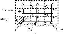
对于目前IC设计中的多层布线技术,可布线区域不再是单元间的一条条的布线通道,而是一个完整的芯片平面。可采用网格方式,把整个芯片平面按行和列划分为若干个称为总体布线单元GRC的区域,然后生成GRC的对偶图,即如图4所示的总体布线图GRG。GRG由Nnr×Nnc个节点和连接这些节点的边构成。与GRCnr,nc对应的节点vnr,nc的坐标为GRCnr,nc的中心点。连接两节点vnr1,nc1和vnr2,nc2的边称为ek;lk表示两节点vnr1,nc1和vnr2,nc2之间的距离,称为ek的长度;Ck表示两节点vnr1,nc1和vnr2,nc2对应的两个GRC相邻的边能够通过的线网的连线数,称为ek的容量。于是,线网中要连通的引脚点Pin就映射成为其所在的GRG中对应的一系列节点。这样,GRG中的一个线网就可以用节点的集合表示,而对一个线网的布线问题则对应于求解GRG中节点集{vnr,nc}的Steiner树问题。For the current multi-layer wiring technology in IC design, the routing area is no longer a wiring channel between units, but a complete chip plane. The grid method can be used to divide the entire chip plane into several regions called the general wiring unit GRC according to the rows and columns, and then generate the dual graph of the GRC, that is, the general wiring diagram GRG shown in Figure 4. GRG consists of Nnr ×Nnc nodes and edges connecting these nodes. The coordinates of node v nr, nc corresponding to GRC nr, nc are the central point of GRCnr, nc . The edge connecting two nodes vnr1, nc1 and vnr2, nc2 is called ek ; lk represents the distance between two nodes vnr1, nc1 and vnr2, nc2 , which is called the length of ek ; Ck represents the length of two nodes vnr1, nc1 and vnr2, nc2 correspond to the number of lines that can pass through the adjacent sides of the two GRCs, which is called the capacity of ek . Therefore, the pin point Pin to be connected in the line network is mapped to a series of corresponding nodes in the GRG where it is located. In this way, a net in GRG can be represented by a set of nodes, and the routing problem for a net corresponds to solving the Steiner tree problem of node set {vnr, nc } in GRG.
本布线方法的流程框图如图5所示。The flow chart of this wiring method is shown in FIG. 5 .
现在采用国际基准测试电路实例MCNC C5作为本发明的一个实施例,结合图5的程序流程用本发明的总体布线方法进行布线。它依次有如下步骤:Now adopt the international benchmark test circuit example MCNC C5 as an embodiment of the present invention, and carry out wiring with the general wiring method of the present invention in conjunction with the program flow of Fig. 5. It has the following steps in order:
(1)初始化:(1) Initialization:
设:行数Nnr=16,列数Nnc=18,如图6所示。此时,GRG图中共有288个顶点,每个顶点都有一个对应的位置坐标(x,y),例如:在图6中,v1,1顶点的位置坐标是(44,122),v1,2顶点的位置坐标是(202,122),即可用vnr,nc(x,y)表示,nr表示GRG上第几行,nc表示GRG上第几列,坐标(x,y)是相对芯片平面的坐标原点而言的;共有542条边,每条边都有一个用户给定的容量,从16~17,例如:连接v1,1与v1,2的边的容量为16,连接v1,2与v1,3的边的容量为16。Assume: the number of rows Nnr =16, the number of columns Nnc =18, as shown in FIG. 6 . At this time, there are 288 vertices in the GRG graph, and each vertex has a corresponding position coordinate (x, y). For example: in Figure 6, the position coordinates of v1, 1 vertex are (44, 122), The position coordinates of vertices1 and 2 are (202, 122), which can be expressed by vnr, nc (x, y), nr indicates the row on the GRG, nc indicates the column on the GRG, and the coordinates (x, y) are Relative to the coordinate origin of the chip plane; there are 542 sides in total, each side has a capacity given by the user, from 16 to 17, for example: the capacity of the side connecting v1,1 and v1,2 is 16 , the capacity of the edge connecting v1, 2 and v1, 3 is 16.
设:线网的总数Nsum为1764条,Suppose: the total number Nsum of the line network is 1764,
设置用户给出的时延约束指标,如其中一个时延值为7.200000ns。Set the delay constraint index given by the user, for example, one of the delay values is 7.200000ns.
(2)生成GRG:(2) Generate GRG:
读入Nnr=16,Nnc=18;按照先行后列的顺序,给288个顶点全部编号,分别为1~288号;再按照先行后列的顺序,从1号顶点开始,把542条GRG边全部编号,分别为1~542号。Read in Nnr = 16, Nnc = 18; according to the order of the first line and then the column, all the 288 vertices are numbered, which are respectively 1 to 288; and then according to the order of the first line and the second column, starting from the vertex No. 1, the 542 All GRG edges are numbered from 1 to 542.
(3)读入电路详细连接关系即网表:(3) Read in the detailed connection relationship of the circuit, that is, the netlist:
读入电路中线网总数Nsum=1764。按照网表读入的顺序,给1764条线网全部编号,分别为net 1~net 1764。于是得到每条线网包含源点、漏点信息在内的网表,其具体形式描述如下:Read in the total number of nets in the circuit Nsum=1764. According to the order in which the netlist is read, all the 1764 nets are numbered, net 1~net 1764 respectively. Then get a netlist including source point and leak point information for each line net, and its specific form is described as follows:
22号线网的网表表示是:(net 22(vertexList 182,2;164,2;128,1)),The netlist representation of No. 22 net is: (net 22(
1764号线网的网表表示是:(net 1764(vertexList 3,2;5,1))。The netlist representation of line 1764 is: (net 1764(
以net 1764为例,它表示的是:第3号顶点是漏点,第5号顶点是源点。它们的通式可表示为:Taking net 1764 as an example, it means that the No. 3 vertex is the leak point, and the No. 5 vertex is the source point. Their general formula can be expressed as:
(net号(VertexList顶点号,源点/漏点;……)),(net number(VertexList vertex number, source/drain;...)),
其中:数字1表示源点,数字2表示漏点。Among them: the
(4)读入电路的所有电学性能参数与约束指标,赋到相应的变量和数组之中:(4) Read in all the electrical performance parameters and constraint indexes of the circuit, and assign them to corresponding variables and arrays:
读入:用户给出的时延约束指标参数赋到数组中,其中一个时延约束指标(从PI到PO)=7.000000ns。Read in: assign the delay constraint index parameters given by the user to the array, and one delay constraint index (from PI to PO)=7.000000ns.
(5)构造初始时延优化的布线树:(5) Construct an initial delay-optimized routing tree:
采用Tree.cpp程序完成。其中采用现有技术“分层Dreyfus-Wagner算法”。它已公开发表于1998年的国内核心期刊:“鲍海云,洪先龙,蔡懿慈等.‘基于Dreyfus-Wagner算法的Steiner树分层构造算法’.《微电子学与计算机》,1998,增刊:41~44”。用该算法求出的初始布线树其形式如下:Use the Tree.cpp program to complete. Wherein the prior art "layered Dreyfus-Wagner algorithm" is adopted. It has been published in domestic core journals in 1998: "Bao Haiyun, Hong Xianlong, Cai Yici, etc. 'A Steiner Tree Hierarchical Construction Algorithm Based on the Dreyfus-Wagner Algorithm'." Microelectronics and Computers, 1998, Supplement: 41-44 ". The form of the initial wiring tree obtained by this algorithm is as follows:
#Init_Steiner_Tree 22#Init_Steiner_Tree 22
((
(connect 128 146)(connect 128 146)
(connect 146 164)(connect 146 164)
(connect 164 182)(connect 164 182)
))
…………………………………………
#Init_Steiner_Tree 1764#Init_Steiner_Tree 1764
((
(connect 3 4)(connect 3 4)
(connect 4 5)(connect 4 5)
))
其通用表达式为:Its general expression is:
#Init_Steiner_Tree XXX#Init_Steiner_Tree XXX
((
(connect顶点号 顶点号)(connect vertex number vertex number)
……………………
(connect顶点号 顶点号)(connect vertex number vertex number)
))
(6)统计总的可用布线资源,标记拥挤区域:(6) Count the total available routing resources and mark the crowded area:
采用Update_Resources.cpp程序完成。统计每条GRG边的被使用量(即有多少线网通过了该边)dk,再把它与允许容量Ck比较,若Ck<dk,则表明出现布线拥挤,把它在结构EdgeIndex中标记为1;把所有经过标记为1的GRG边的线网确定为拥挤线网。Use the Update_Resources.cpp program to complete. Count the used amount of each GRG side (that is, how many lines have passed the side) dk , and then compare it with the allowable capacity Ck , if Ck <dk , it indicates that there is wiring congestion, put it in the structure Marked as 1 in EdgeIndex; all line nets passing through the GRG edge marked as 1 are determined as crowded nets.
本实施例中,共标记出221条布线拥挤的GRG边,598个拥挤线网。In this embodiment, a total of 221 GRG edges and 598 crowded nets are marked.
(7)优化布线拥挤,消除拥挤边:(7) Optimize wiring congestion and eliminate crowded edges:
采用SSTT.cpp程序完成。其中采用了“基于搜索空间遍历技术(SSTT)的布线拥挤优化算法”,它已公开发表于2001年的国际学术会议:“Tong Jing,Xian-Long Hong,Hai-Yun Bao,et al.‘An Efficient Congestion Optimization Algorithm for Global Routing Based onSearch Space Traversing Technology’.In Proceedings of IEEE ASICON,2001,114~117”。Use SSTT.cpp program to complete. Among them, the "Wiring Congestion Optimization Algorithm Based on Search Space Traversal Technology (SSTT)" was used, which was published in the international academic conference in 2001: "Tong Jing, Xian-Long Hong, Hai-Yun Bao, et al.'An Efficient Congestion Optimization Algorithm for Global Routing Based on Search Space Traversing Technology'. In Proceedings of IEEE ASICON, 2001, 114~117".
在本实施例中,进行布线拥挤的优化后,消除了全部拥挤边。In this embodiment, after the routing congestion optimization is performed, all the crowded edges are eliminated.
(8)统计电路时延信息:(8) Statistical circuit delay information:
采用Coll_Timing_Info.cpp程序完成。根据步骤(7)执行后的布线结果进行时延计算,得到每条电信号传输路径从输入PI到输出PO的时延值。所采用的模型为公知的“SAKURAI时延计算公式”。Use the Coll_Timing_Info.cpp program to complete. The time delay is calculated according to the wiring result after step (7) is executed, and the time delay value of each electrical signal transmission path from the input PI to the output PO is obtained. The adopted model is the well-known "SAKURAI delay calculation formula".
最后,把用户时延约束指标与上述计算出的每条电信号传输路径的延迟值进行比较,分析得到此时时延不满足用户要求的关键路径。Finally, compare the user delay constraint index with the delay value of each electrical signal transmission path calculated above, and analyze the critical path whose delay does not meet the user's requirements at this time.
(9)优化电路时延:(9) Optimize circuit delay:
用BO_Timing.cpp程序完成。首先,利用关键网络概念[已申请的国家发明专利:洪先龙,经彤,鲍海云,蔡懿慈,许静宇.发明名称:基于关键网络技术优化时延的标准单元总体布线方法.申请日期:2002/01/15.申请号为:02100354.8.已于2002/07/24被公开,于2004/05/19被授权],为电路构造关键网络。Complete with BO_Timing.cpp program. First, use the key network concept [National invention patents that have been applied for: Hong Xianlong, Jing Tong, Bao Haiyun, Cai Yici, Xu Jingyu. Invention name: Standard cell overall wiring method based on key network technology to optimize time delay. Application date: 2002/01/15 .The application number is: 02100354.8. It was published on 2002/07/24 and authorized on 2004/05/19], which is a key network for circuit construction.
下面对关键网络概念进行简单的介绍:在集成电路中,电信号的传递有2种形式:(1)信号在单元内部传递:信号由单元的一个或多个输入pin,经过单元内部的逻辑变换,传递到单元的输出pin;(2)信号在单元之间传递:以单元的输出pin为源点,经过线网对应的布线树传递到其他一些单元的输入pin。如果将电路单元的端口看成是顶点,将信号在单元内部和单元之间的传递看成是连接顶点的边,以信号传递的时延作为边的权值,再增加虚拟的电路总输入s和总输出t,则逻辑电路可以自然地转化为一个网络结构。其中为了方便表示,加入两个虚拟的顶点:源点s表示虚拟的电路总输入,汇点t表示虚拟的电路总输出。The following is a brief introduction to key network concepts: In integrated circuits, there are two forms of electrical signal transmission: (1) Signal transmission within the unit: the signal is transmitted from one or more input pins of the unit to the logic inside the unit Transformation, transmitted to the output pin of the unit; (2) The signal is transmitted between the units: the output pin of the unit is used as the source point, and it is transmitted to the input pins of some other units through the wiring tree corresponding to the wire network. If the port of the circuit unit is regarded as a vertex, the transmission of signals inside and between the units is regarded as the edge connecting the vertex, and the delay of signal transmission is used as the weight of the edge, and then the virtual circuit total input s is added and the total output t, the logic circuit can be naturally transformed into a network structure. For the convenience of representation, two virtual vertices are added: the source point s represents the total input of the virtual circuit, and the sink point t represents the total output of the virtual circuit.
对网络中的某一个顶点i,其总是对应一对数值:最早到达时间tE(i)和最迟到达时间tL(i),分别表示信号从源点传递到该顶点的实际时间,以及信号为了满足时延约束而必须到达该顶点的最迟时间。于是,可以设想:汇点t的最早到达时间对应的是整个电路的总时延,它决定了整个电路的速度,记为TE。同时,电路设计者要对整个电路的速度加以控制,提出总时延要求,称为要求的总时延,记为TL。若某顶点i的最早到达时间大于其最迟到达时间,即满足tE(i)>tL(i),称该顶点为关键pin;若两顶点i、k之间存在边,delay(i,k)表示它们之间的时延,且tE(i)+delay(i,k)>tL(k),则称边(i,k)为关键边。关键网络理论证明了若TE>TL,时延传递网络中存在着由且仅由关键pin和关键边构成的子网络N,N=(V,E,d,s,t)。其中:V为关键pin的集合,E为关键边的集合,d为有向边对应的时延值。该子网络N称为关键网络,它反映了当前对电路总时延影响最大的子网络的时延情况。For a certain vertex i in the network, it always corresponds to a pair of values: the earliest arrival time tE (i) and the latest arrival time tL (i), which respectively represent the actual time when the signal is transmitted from the source point to the vertex, and the latest time the signal must arrive at the vertex in order to satisfy the delay constraint. Therefore, it can be imagined that the earliest arrival time of the sink point t corresponds to the total delay of the entire circuit, which determines the speed of the entire circuit, denoted asTE . At the same time, the circuit designer needs to control the speed of the entire circuit and put forward the total delay requirement, which is called the required total delay, denoted as TL . If the earliest arrival time of a vertex i is greater than its latest arrival time, which satisfies tE (i) > tL (i), the vertex is called a key pin; if there is an edge between two vertices i and k, delay(i , k) represents the delay between them, and tE (i)+delay(i, k)>tL (k), then the edge (i, k) is called a key edge. The key network theory proves that if TE >TL , there exists a sub-network N consisting only of key pins and key edges in the delay transfer network, N=(V, E, d, s, t). Among them: V is the set of key pins, E is the set of key edges, and d is the delay value corresponding to the directed edge. The sub-network N is called a key network, which reflects the current delay situation of the sub-network that has the greatest impact on the total circuit delay.
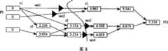
本实施例中,建立了一个包含全部396个关键pin、198条关键边的关键网络,其局部如图7所示。在图7中,共有30个关键pin、15条关键边。其中,从PI到路径中每个门的输出pin的最早到达时间已在该门(图7中的方框)中标出,即:图7中方框所标出的延迟值都是以PI为起始点到门的输出pin的延迟值,单位为纳秒(ns)。在图7中,从PI到PO的延迟为7.359ns。与要求满足的时延约束指标7.000000ns相比,超出了0.359ns。In this embodiment, a key network including all 396 key pins and 198 key edges is established, a part of which is shown in FIG. 7 . In Figure 7, there are 30 key pins and 15 key edges. Among them, the earliest arrival time from PI to the output pin of each gate in the path has been marked in the gate (the box in Figure 7), that is, the delay values marked in the box in Figure 7 are all starting from PI The delay value from the start point to the output pin of the gate, in nanoseconds (ns). In Figure 7, the delay from PI to PO is 7.359ns. Compared with the required delay constraint index of 7.000000ns, it exceeds 0.359ns.
为了从关键网络中选择一组边对应的线网进行时延优化,我们利用了“图与网络规划理论”中的“最大流与最小割关系定理”(属于现有技术,王永县 编著,《运筹学——规划论及网络》中的第五章,清华大学出版社,1993)。挑选每个线网在拥挤优化中得到的时延最好的布线树,作为该线网的时延最优布线树。假设将网络中的某边所对应线网的布线树替换为时延最优布线树后,该边的时延改进量为Δd(Δd为正数表示时延改善),拥挤度代价的改进量为Δc(Δc为正数表示拥挤度改善),则按照如下方法设定时延改进权值:如果当前布线树就是时延最优布线树,设定权值为1,表示单纯更换布线树后时延参数不能得到优化,但可以通过插入缓冲器得到改善;如果时延最优布线树Δd>0且Δc>0,则权值为0,表示更换布线树有利于对时延和拥挤度的同时优化;如果Δd>0而Δc<0,则权值为Δc2/Δd,表示以一定的拥挤度劣化为代价换取对时延的优化。通过求解关键网络中的最小割的方法,可以得到关键网络中对时延优化作用最明显,而对拥挤劣化最小的一组线网,如图8虚线所示。其中,有1个多端点线网,由net1标识,其源点为s1,有3个漏点,分别为t1、t2、t3;有3个两端点线网,分别由net2、net3、net4标识。两端点线网net2、net3、net4的布线树的形状为直线连接;多端点线网net1的布线树的形状如图9所示(注:在总体布线工艺阶段,不同漏点,如t1与t3可用形如图中的布线树连接,反映的是大致走线趋势)。In order to select a line network corresponding to a group of edges from the key network for time delay optimization, we have utilized the "Maximum Flow and Minimum Cut Relation Theorem" in "Graph and Network Planning Theory" (belonging to the prior art, edited by Wang Yongxian, Chapter 5 in "Operational Research - Planning and Networks", Tsinghua University Press, 1993). The routing tree with the best delay obtained in the congestion optimization for each net is selected as the delay-optimized routing tree for the net. Assuming that after replacing the wiring tree corresponding to a certain edge in the network with a delay-optimized wiring tree, the delay improvement of this edge is Δd (Δd is a positive number indicating delay improvement), and the improvement of congestion cost is Δc (a positive number of Δc indicates that the congestion degree is improved), then set the delay improvement weight according to the following method: If the current wiring tree is the delay optimal wiring tree, set the weight to 1, which means that after simply replacing the wiring tree The delay parameter cannot be optimized, but it can be improved by inserting buffers; if the delay optimal routing tree Δd>0 and Δc>0, then the weight is 0, which means that replacing the routing tree is beneficial to delay and congestion Simultaneous optimization; if Δd>0 and Δc<0, then the weight is Δc2 /Δd, which means that the optimization of the time delay is obtained at the cost of a certain degree of congestion degradation. By solving the minimum cut method in the key network, a group of line networks that have the most obvious effect on delay optimization and the least congestion degradation in the key network can be obtained, as shown by the dotted line in Figure 8. Among them, there is 1 multi-terminal line network, identified by net1, its source point is s1, and there are 3 leakage points, namely t1, t2, t3; there are 3 end-point line networks, respectively identified by net2, net3, net4 . The shape of the wiring tree of net2, net3, and net4 with two ends is a straight line connection; the shape of the wiring tree of net1 with multi-ends is shown in Figure 9 (Note: In the overall wiring process stage, different leak points, such as t1 and t3 It can be connected with the wiring tree in the figure, which reflects the general wiring trend).
将这些线网的布线树替换为各自的时延最优布线树。其中,两端点线网net2、net3、net4的时延最优布线树的形状仍为直线连接;多端点线网net1的时延最优布线树的形状如图10所示。Replace the routing trees for these nets with their respective delay-optimized routing trees. Among them, the shape of the delay-optimized wiring tree of the two-end line net2, net3, and net4 is still a straight line connection; the shape of the delay-optimized wiring tree of the multi-end line net1 is shown in FIG. 10 .
然后,进行缓冲器插入,其插入位置由前面推导的最优位置公式计算可得。在本实施例中涉及的电学参数取值如下表:Then, the buffer is inserted, and its insertion position is calculated by the optimal position formula deduced above. The values of the electrical parameters involved in this embodiment are as follows:
表5本实施例中涉及的电学参数取值
以两端点线网net3为例,其包含一个源点和一个漏点,因此该漏点即为关键漏点。源点到关键漏点的连线长为l=9360um(微米)。由于net3源点、漏点满足:源点驱动电阻Rs等于缓冲器输出电阻rb;漏点负载电容Ct等于缓冲器输入电容cb,根据前述对两端点线网插入缓冲器的最优位置的推导,最优插入位置为源点到关键漏点的连线的1/2处,即l1=l2=l/2。则缓冲器的插入位置为距离源点4680um处。Take the two-point net3 as an example, it contains a source point and a leak point, so this leak point is a key leak point. The line length from the source point to the critical drain point is l=9360um (micrometer). Since the source point and drain point of net3 satisfy: the driving resistance Rs of the source point is equal to the output resistance rb of the buffer; the load capacitance Ct of the drain point is equal to the input capacitance cb of the buffer, according to the above-mentioned optimal For position derivation, the optimal insertion position is 1/2 of the line connecting the source point to the key drain point, that is, l1 =l2 =l/2. Then the insertion position of the buffer is 4680um away from the source point.
设插入缓冲器前t点的时延为D,插入缓冲器后时延为D’,将表5中的电学参数代入前面根据SAKURAI时延计算公式推导的结果,有:Let the time delay at point t before inserting the buffer be D, and the time delay after inserting the buffer be D’, and substitute the electrical parameters in Table 5 into the result derived from the calculation formula of SAKURAI time delay, as follows:
D=βRs(l1c+l2c+Ct)+αrc(l1+l2)2+βr(l1+l2)CtD=βRs (l1 c+l2 c+Ct )+αrc(l1 +l2 )2 +βr(l1 +l2 )Ct
=0.4917+0.7909+0.0124=1.2950ns(纳秒)=0.4917+0.7909+0.0124=1.2950ns (nanosecond)
而根据(1)式,And according to formula (1),
D-D′=βcl2(Rs-rb)+βCt(Rs-rb)+βrl1(Ct-cb)+2αrcl1l2-βRscb-dbDD'=βcl2 (Rs -rb )+βCt (Rs -rb )+βrl1 (Ct -cb )+2αrcl1 l2 -βRs cb -db
=0.3954-0.0035-0.0364=0.3555ns= 0.3954-0.0035-0.0364 = 0.3555 ns
因此:D’=D-0.3555=0.9395nsTherefore: D'=D-0.3555=0.9395ns
net3插入缓冲器前的关键漏点时延为1.2950ns(纳秒),插入缓冲器后的关键漏点时延为0.9395ns,时延改善量为0.3555ns。The delay of the key leak point before net3 is inserted into the buffer is 1.2950ns (nanosecond), the delay of the key leak point after inserting the buffer is 0.9395ns, and the delay improvement is 0.3555ns.
对于多端点线网net1,其源点为s1,关键漏点为t1,源点到关键漏点的连线长为l=7584um,依次按照下述步骤来计算插入缓冲器的最优位置:For the multi-terminal network net1, the source point is s1, the key leak point is t1, and the length of the line from the source point to the key leak point is l=7584um, follow the steps below to calculate the optimal position of inserting the buffer:
一)计算缓冲器在源点到关键漏点的路径上插入时的最优位置,包含以下4个步骤:1) Calculating the optimal position of the buffer when it is inserted on the path from the source point to the critical drain point, including the following 4 steps:
1)根据关键漏点t1的位置,将多端线网net1的时延最优布线树转化为带有分支的源点到t1的路径表示。如图11所示,该路径有两个分支,路径和分支的位置及长度在图中标出。1) According to the location of the key leakage point t1, the delay optimal routing tree of the multi-terminal net1 is transformed into a path representation from the source point to t1 with branches. As shown in Figure 11, the path has two branches, and the positions and lengths of the paths and branches are marked in the figure.
2)计算每个分支的电容。2) Calculate the capacitance of each branch.
分支电容=分支上的连线电容+分支的负载电容Branch capacitance = wiring capacitance on the branch + load capacitance of the branch
=分支长度×单位线电容+分支的负载电容= branch length × unit line capacitance + load capacitance of the branch
将表5中的电学参数和分支的长度代入上式,可得:Substituting the electrical parameters and branch lengths in Table 5 into the above formula, we can get:
分支1电容C1=234um×0.118fF/μm=0.0276pf(皮法)
分支2电容C2=234um×0.118fF/μm=0.0276pf(皮法)
3)对每个Ci与Ci+1之间的区域,按照式(8)计算缓冲器与源点的最优插入距离x。如果x不落在该区域内,则选择区域两端点中靠近x的端点作为本区域最优插入位置。3) For each region between Ci and Ci+1 , calculate the optimal insertion distance x between the buffer and the source according to formula (8). If x does not fall within the area, select the end point close to x among the two end points of the area as the optimal insertion position in this area.
图11所示的路径有两个分支,将路径分为3段,下面分别计算每个区域对应的缓冲器插入位置:The path shown in Figure 11 has two branches, and the path is divided into three sections. The buffer insertion position corresponding to each area is calculated as follows:
3-1)s1与分支1之间的区域3-1) Area between s1 and
根据前述对多端点线网插入缓冲器的最优位置的推导,According to the above-mentioned derivation of the optimal position for inserting buffers of multi-terminal nets,
将表5中电学参数代入(8)式,可得本区域中最优插入距离为Substituting the electrical parameters in Table 5 into formula (8), the optimal insertion distance in this area can be obtained as
由于该区域范围为0到316um,x不落在该区域内,则选择区域两端点中靠近x的端点,即分支1与路径的交点u1作为本区域最优插入位置,即:x=316umSince this area ranges from 0 to 316um, and x does not fall within this area, select the end point close to x among the two ends of the area, that is, the intersection point u1 between
32)分支1与分支2之间的区域32) The area between
根据前述对多端点线网插入缓冲器的最优位置的推导,According to the above-mentioned derivation of the optimal position for inserting buffers of multi-terminal nets,
将表5中电学参数代入(8)式,可得本区域中最优插入距离为Substituting the electrical parameters in Table 5 into formula (8), the optimal insertion distance in this area can be obtained as
由于该区域范围为316到790um,x不落在该区域内,则选择区域两端点中靠近x的端点,即分支2与路径的交点u2作为本区域最优插入位置,即:x=790um。Since this area ranges from 316 to 790um, and x does not fall within this area, select the end point close to x among the two end points of the area, that is, the intersection point u2 between
3-3)分支2与t1之间的区域3-3) The area between
根据前述对多端点线网插入缓冲器的最优位置的推导,According to the above-mentioned derivation of the optimal position for inserting buffers of multi-terminal nets,
将表5中电学参数代入(8)式,可得本区域中最优插入距离为Substituting the electrical parameters in Table 5 into formula (8), the optimal insertion distance in this area can be obtained as
由于该区域范围为790到7584um,x落在该区域内,x为本区域最优插入位置,即:x=3791um。Since this area ranges from 790 to 7584um, x falls within this area, and x is the optimal insertion position in this area, ie: x=3791um.
4)计算每个区域最优插入位置的时延改善量,选择取得最大值的位置作为s1到t1路径上的最优插入点。4) Calculate the delay improvement of the optimal insertion position in each area, and select the position with the maximum value as the optimal insertion point on the path from s1 to t1.
将上述三个区域求得的插入点位置x分别代入(7)式,求得时延改善量D-D’:Substitute the position x of the insertion point obtained in the above three areas into equation (7) to obtain the delay improvement D-D':
4-1)对于s1与分支1之间的区域,Cll=0.0632pf,x=316um,时延改善量为:4-1) For the area between s1 and
D-D′=-βrcx2+[βr(lc+Cll-cb)-β(Rs-rb)c]x+[β(Rs-rb)(lc+Cll)-(βRscb+db)]DD′=-βrcx2 +[βr(lc+Cll -cb )-β(Rs -rb )c]x+[β(Rs -rb )(lc+Cll )-(βRs cb +db )]
=-0.00195+0.04976-0.03994=0.00787ns=-0.00195+0.04976-0.03994=0.00787ns
4-2)对于分支1与分支2之间的区域,Cll=0.0356pf,x=790um,时延改善量为:4-2) For the area between
D-D′=-βrcx2+[βr(lc+Cll-cb)-β(Rs-rb)c]x+[β(Rs-rb)(lc+Cll)-(βRscb+db)]DD′=-βrcx2 +[βr(lc+Cll -cb )-β(Rs -rb )c]x+[β(Rs -rb )(lc+Cll )-(βRs cb +db )]
=-0.01221+0.12080-0.03994=0.06865ns=-0.01221+0.12080-0.03994=0.06865ns
4-3)对于分支2与t1之间的区域,Cll=0.008pf,x=3791um,时延改善量为:4-3) For the area between
D-D′=-βrcx2+[βr(lc+Cll-cb)-β(Rs-rb)c]x+[β(Rs-rb)(lc+Cll)-(βRscb+db)]DD′=-βrcx2 +[βr(lc+Cll -cb )-β(Rs -rb )c]x+[β(Rs -rb )(lc+Cll )-(βRs cb +db )]
=-0.28109+0.56233-0.03994=0.24130ns=-0.28109+0.56233-0.03994=0.24130ns
取得时延改善量最大值的位置为分支2与t1之间的区域。即:当插入点位于s1到t1路径上时,最优插入位置为距离源点x=3791um处,时延改善量为0.24130ns。The position where the maximum delay improvement is obtained is the area between
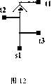
二)计算缓冲器在分支点插入的最优位置。2) Calculating the optimal position where the buffer is inserted at the branch point.
根据前面的推导,缓冲器在分支点插入时,最大的时延改善由
对于分支1,

对于分支2,

取得时延改善量最大值的位置为分支2。即:当插入点位于分支点时,最优插入位置为分支2上,时延改善量为0.01123ns。
三)将s1到t1路径上的最优插入点的时延改善量与最优分支插入点的时延改善进行比较,选择取得最大值的位置作为最终的插入点。3) Compare the delay improvement of the optimal insertion point on the path from s1 to t1 with the delay improvement of the optimal branch insertion point, and select the position with the maximum value as the final insertion point.
通过对(一)和(二)计算结果的比较,可得:最优插入位置为s1到t1路径上,插入位置为距离源点x=3791um处,插入位置如图12所示。时延改善量为0.24130ns,从而达到了时延优化的目的。按照上述过程,依次对关键网络割线上的线网进行缓冲器插入的时延优化,其优化后的时延值在图13标出。这时,从PI到PO的延迟为6.585ns,小于时延约束指标7.000000ns。于是,实现了电路的时延优化。By comparing the calculation results of (1) and (2), it can be obtained that the optimal insertion position is on the path from s1 to t1, and the insertion position is at a distance of x=3791um from the source point. The insertion position is shown in Figure 12. The amount of time delay improvement is 0.24130ns, thereby achieving the purpose of time delay optimization. According to the above process, delay optimization of buffer insertion is performed on the line nets on the secant line of the key network in turn, and the optimized delay values are shown in Fig. 13 . At this time, the delay from PI to PO is 6.585ns, which is less than the delay constraint index of 7.000000ns. Thus, the time delay optimization of the circuit is realized.
实施系统implementation system
为了实现,或者说是具体实施本项发明,我们给出以下关于发明实施的描述。In order to realize, or specifically implement the present invention, we give the following description about the implementation of the invention.
实施本发明的计算机系统:本发明所设计的总体布线软件要在一个具体的计算机系统上得以实施,该计算机系统具体描述如下。Computer system implementing the present invention: the general wiring software designed in the present invention will be implemented on a specific computer system, and the computer system is specifically described as follows.
一台Sun公司的V880型工作站;A Sun V880 workstation;
Unix操作系统;Unix operating system;
标准C编程语言;Standard C programming language;
Vi编辑器、gcc编译器、gdb调试工具等。Vi editor, gcc compiler, gdb debugging tool, etc.
本发明方法效果的实验数据The experimental data of the method effect of the present invention
进行实验的计算机系统具体描述如下:The computer system for the experiment is described in detail as follows:
一台Sun公司的V880型工作站;A Sun V880 workstation;
Unix操作系统;Unix operating system;
标准C编程语言;Standard C programming language;
Vi编辑器、gcc编译器、gdb调试工具等;Vi editor, gcc compiler, gdb debugging tool, etc.;
以国际基准测试电路MCNC中的5个实例作为测试例子,我们将本发明方法与已有的基于拓扑优化的总体布线算法CNB的测试结果进行了比较。CNB已公开发表于2002年的国际学术会议:“Tong Jing,Xian-Long Hong,Hai-Yun Bao et al “A Novel and EfficientTiming-Driven Global Router for Standard Cell Layout Design Based on Critical NetworkConcept”in:Proc.IEEE ISCAS,2002,Scottsdale,Arizona,USA,I 165-I 168.”。Taking five examples in the international benchmark test circuit MCNC as test examples, we compared the test results of the method of the present invention with the existing overall routing algorithm CNB based on topology optimization. CNB has been publicly published in the international academic conference in 2002: "Tong Jing, Xian-Long Hong, Hai-Yun Bao et al "A Novel and EfficientTiming-Driven Global Router for Standard Cell Layout Design Based on Critical Network Concept" in: Proc. IEEE ISCAS, 2002, Scottsdale, Arizona, USA, I 165-I 168.”.
表1给出了两个算法的时延性能比较,其中,“CNB”表示上述的已有算法,“Buffer”表示本发明提出的插入缓冲器进行时延优化的总体布线算法。表中比较了要求的电路总时延相对于布线结果的电路总时延的增量。实验数据中“-”表示要求的电路总时延小于布线结果的电路总时延,即电路优化没有满足时延约束(电路总时延超过了给定的时延约束)。表1同时给出了插入缓冲器的数目。Table 1 shows the comparison of the delay performance of the two algorithms, wherein "CNB" indicates the above-mentioned existing algorithm, and "Buffer" indicates the overall wiring algorithm for inserting buffers for delay optimization proposed by the present invention. The table compares the increase in the total circuit delay required relative to the total circuit delay of the routing result. "-" in the experimental data indicates that the total circuit delay required is less than the total circuit delay of the wiring result, that is, the circuit optimization does not meet the delay constraint (the total circuit delay exceeds the given delay constraint). Table 1 also gives the number of inserted buffers.
表1电路时延性能比较
[1]“CNB”:已有算法[1] "CNB": existing algorithm
[2]“Buffer”:本发明提出的插入缓冲器进行时延优化的总体布线算法[2] "Buffer": The overall wiring algorithm for inserting buffers for delay optimization proposed by the present invention
[3]%占单元数百分比:插入缓冲器数目/电路单元数*100%[3]% of the number of units: the number of inserted buffers / the number of circuit units * 100%
从表1可以看出,在一定的时延约束下,如果仅凭借基于拓扑的时延优化手段,电路时延很可能大于要求的总时延而无法得到进一步优化。而插入缓冲器进行时延优化的总体布线算法能够以很少量的缓冲器数目为代价,有效地对电路总时延进行控制和改善。算法要求的缓冲器数目相对于电路单元数而言非常有限,因而可以在完全可接受的缓冲器数目代价下换取时延的明显改善。It can be seen from Table 1 that under certain delay constraints, if only topology-based delay optimization is used, the circuit delay is likely to be greater than the required total delay and cannot be further optimized. However, the overall routing algorithm that inserts buffers for delay optimization can effectively control and improve the total circuit delay at the cost of a small number of buffers. The number of buffers required by the algorithm is very limited relative to the number of circuit units, so a significant improvement in time delay can be exchanged at a fully acceptable cost of the number of buffers.
我们在表2中给出两种算法运行时间的比较。从表中可以看出,插入缓冲器进行时延优化的总体布线算法相对于传统算法,可以在更短的运行时间内获得突出改善的时延优化结果。We give a comparison of the running times of the two algorithms in Table 2. It can be seen from the table that compared with the traditional algorithm, the overall routing algorithm for inserting buffers for delay optimization can obtain significantly improved delay optimization results in a shorter running time.
表2运行时间比较
拥挤优化也是总体布线的优化目标之一。表3给出了两种算法布线结果的拥挤边数,可以看出缓冲器插入算法的拥挤边数与传统算法基本相当。两算法的线长性能比较在表4中给出,两算法对互连线长具有近似的优化能力。Congestion optimization is also one of the optimization goals of overall routing. Table 3 shows the number of crowded edges of the wiring results of the two algorithms. It can be seen that the number of crowded edges of the buffer insertion algorithm is basically equivalent to that of the traditional algorithm. The line length performance comparison of the two algorithms is given in Table 4, and the two algorithms have approximate optimization capabilities for the interconnection line length.
表3拥挤边数比较
表4线长性能比较
[1]%相对CNB线长增量:(本发明方法的线长-CNB方法的线长)/CNB方法的线长*100%[1]% relative CNB line length increment: (the line length of the inventive method-the line length of the CNB method)/the line length of the CNB method*100%
从上述测试结果对比可以看出:本发明方法可以在短时间内以较小的缓冲器插入数目取得很好的时延优化结果,而同时拥挤优化质量也较好。From the comparison of the above test results, it can be seen that the method of the present invention can achieve good delay optimization results with a small number of buffer insertions in a short period of time, and at the same time, the congestion optimization quality is also good.
实验证明它达到了预期目的。Experiments prove that it has achieved the intended purpose.
Claims (1)


Priority Applications (1)
| Application Number | Priority Date | Filing Date | Title |
|---|---|---|---|
| CNB2005100117124ACN100347710C (en) | 2005-05-13 | 2005-05-13 | Standard unit overall wiring method of multi-terminal network plug-in buffer optimizing delay |
Applications Claiming Priority (1)
| Application Number | Priority Date | Filing Date | Title |
|---|---|---|---|
| CNB2005100117124ACN100347710C (en) | 2005-05-13 | 2005-05-13 | Standard unit overall wiring method of multi-terminal network plug-in buffer optimizing delay |
Publications (2)
| Publication Number | Publication Date |
|---|---|
| CN1687934A CN1687934A (en) | 2005-10-26 |
| CN100347710Ctrue CN100347710C (en) | 2007-11-07 |
Family
ID=35305975
Family Applications (1)
| Application Number | Title | Priority Date | Filing Date |
|---|---|---|---|
| CNB2005100117124AExpired - Fee RelatedCN100347710C (en) | 2005-05-13 | 2005-05-13 | Standard unit overall wiring method of multi-terminal network plug-in buffer optimizing delay |
Country Status (1)
| Country | Link |
|---|---|
| CN (1) | CN100347710C (en) |
Families Citing this family (13)
| Publication number | Priority date | Publication date | Assignee | Title |
|---|---|---|---|---|
| US8595674B2 (en) | 2007-07-23 | 2013-11-26 | Synopsys, Inc. | Architectural physical synthesis |
| US8819608B2 (en) | 2007-07-23 | 2014-08-26 | Synopsys, Inc. | Architectural physical synthesis |
| CN101452496B (en)* | 2007-12-06 | 2010-09-22 | 英业达股份有限公司 | Method for acquiring layout path of signal line |
| US8307315B2 (en) | 2009-01-30 | 2012-11-06 | Synopsys, Inc. | Methods and apparatuses for circuit design and optimization |
| CN103632001B (en)* | 2013-11-27 | 2016-03-30 | 中国人民解放军国防科学技术大学 | Based on the retention time timing optimization method that buffer cell is multiplexing |
| CN103617321B (en)* | 2013-11-27 | 2016-06-08 | 中国人民解放军国防科学技术大学 | Reduce the method for different end angles lower bumper chain time delay change |
| CN109800495B (en)* | 2019-01-14 | 2023-05-02 | 深圳忆联信息系统有限公司 | Clock tree optimization method and device based on DDR PHY physical implementation |
| CN112417803B (en)* | 2020-12-02 | 2024-02-06 | 苏州复鹄电子科技有限公司 | Automatic optimization method for design parameters of analog integrated circuit based on artificial intelligence algorithm |
| CN113011124B (en)* | 2021-04-12 | 2024-01-26 | 上海伴芯科技有限公司 | Crosstalk optimization method and device for layout wiring and readable storage medium |
| CN114239444B (en)* | 2021-12-21 | 2023-08-29 | 东南大学 | A Block-Based Method for Establishing Circuit Delay Model |
| CN116070575B (en)* | 2023-01-12 | 2023-08-15 | 广东工业大学 | Chip wiring optimization method and software system |
| CN116663480B (en)* | 2023-06-19 | 2024-07-09 | 北京华大九天科技股份有限公司 | Method for generating shielding wire of ultra-large scale integrated circuit layout |
| CN117454832B (en)* | 2023-10-10 | 2024-06-11 | 北京市合芯数字科技有限公司 | Wiring method, device, equipment and medium for data channel in circuit chip |
Citations (7)
| Publication number | Priority date | Publication date | Assignee | Title |
|---|---|---|---|---|
| US5491641A (en)* | 1993-10-04 | 1996-02-13 | Lsi Logic Corporation | Towards optical steiner tree routing in the presence of rectilinear obstacles |
| US5737237A (en)* | 1995-02-17 | 1998-04-07 | Matsushita Electric Industrial Co., Ltd. | Method and apparatus for data path circuit layout design and memory medium for causing computer to execute data path circuit layout design |
| US5764532A (en)* | 1995-07-05 | 1998-06-09 | International Business Machines Corporation | Automated method and system for designing an optimized integrated circuit |
| US5778216A (en)* | 1995-06-30 | 1998-07-07 | Cadence Design Systems, Inc. | Method for hierarchical time drive circuit layout by rebudgeting timing constraints of plurality of logical blocks after placement |
| CN1360268A (en)* | 2002-01-15 | 2002-07-24 | 清华大学 | Over-all wiring method for standard units based on optimized time delay and key network techniques |
| CN1416082A (en)* | 2002-12-17 | 2003-05-07 | 清华大学 | Integrated wiring method of standard units with carrying optimization of time delay based on considering coupling effect |
| CN1472680A (en)* | 2003-05-01 | 2004-02-04 | 清华大学 | Crosstalk reduction method used in standard cell overall wiring process |
- 2005
- 2005-05-13CNCNB2005100117124Apatent/CN100347710C/ennot_activeExpired - Fee Related
Patent Citations (8)
| Publication number | Priority date | Publication date | Assignee | Title |
|---|---|---|---|---|
| US5491641A (en)* | 1993-10-04 | 1996-02-13 | Lsi Logic Corporation | Towards optical steiner tree routing in the presence of rectilinear obstacles |
| US5880970A (en)* | 1993-10-04 | 1999-03-09 | Lsi Logic Corporation | Towards optimal Steiner tree routing in the presence of rectilinear obstacles |
| US5737237A (en)* | 1995-02-17 | 1998-04-07 | Matsushita Electric Industrial Co., Ltd. | Method and apparatus for data path circuit layout design and memory medium for causing computer to execute data path circuit layout design |
| US5778216A (en)* | 1995-06-30 | 1998-07-07 | Cadence Design Systems, Inc. | Method for hierarchical time drive circuit layout by rebudgeting timing constraints of plurality of logical blocks after placement |
| US5764532A (en)* | 1995-07-05 | 1998-06-09 | International Business Machines Corporation | Automated method and system for designing an optimized integrated circuit |
| CN1360268A (en)* | 2002-01-15 | 2002-07-24 | 清华大学 | Over-all wiring method for standard units based on optimized time delay and key network techniques |
| CN1416082A (en)* | 2002-12-17 | 2003-05-07 | 清华大学 | Integrated wiring method of standard units with carrying optimization of time delay based on considering coupling effect |
| CN1472680A (en)* | 2003-05-01 | 2004-02-04 | 清华大学 | Crosstalk reduction method used in standard cell overall wiring process |
Also Published As
| Publication number | Publication date |
|---|---|
| CN1687934A (en) | 2005-10-26 |
Similar Documents
| Publication | Publication Date | Title |
|---|---|---|
| CN100347710C (en) | Standard unit overall wiring method of multi-terminal network plug-in buffer optimizing delay | |
| CN1253790C (en) | Display device and driving method thereof | |
| CN1529864A (en) | Method and japparatus for considering diagonal wiring in placement | |
| CN1254994C (en) | Network topologies | |
| CN1275178C (en) | Method for setting design margin for LSI | |
| CN1801160A (en) | Method and system for technology migration of integrated circuits with fundamental design constraints | |
| CN1258729C (en) | Large-scale hybrid mode layout method based on virtual module | |
| CN1279480C (en) | An overall routing method for standard cells with time delay optimization considering coupling effects | |
| CN1886744A (en) | Method and apparatus for adding advanced instructions in an extensible processor architecture | |
| CN100336066C (en) | Resistance value calculation method | |
| CN1379346A (en) | Digital content entering system and digital content entering program | |
| CN1304996C (en) | Rectangular steiner tree method of super large size integrated circuit avoiding barrier | |
| CN1102260C (en) | Method, system, equipment and multiplier for automatic design of logic circuit | |
| CN101064302A (en) | Semiconductor device and semiconductor device layout designing method | |
| CN1431704A (en) | Solving method for transient analysis of power source network based on equivalent circuit | |
| CN1779686A (en) | Techniqes for making sure of buffer insertion | |
| CN101034808A (en) | Distributed computing method of the features of the power system | |
| CN1862546A (en) | Fast method for analyzing IC wiring possibility | |
| CN1273878C (en) | Semiconductor equipment | |
| CN1275317C (en) | Integrated circuit layout plan and buffer plan integrated layout method | |
| CN1624698A (en) | High-order synthesis method and high-order synthesis device | |
| CN1275318C (en) | High speed high precision transient simulation method able to process tree net hybrid power supply structure in VLSI | |
| CN1271553C (en) | Generally distributing method of standant unit for eliminating crosstalk caused by coupling inductance | |
| CN1540745A (en) | Method for designing low-power semiconductor integrated circuits | |
| CN100336065C (en) | Right angle wiring tree method for wire length optimized obstacle passing |
Legal Events
| Date | Code | Title | Description |
|---|---|---|---|
| C06 | Publication | ||
| PB01 | Publication | ||
| C10 | Entry into substantive examination | ||
| SE01 | Entry into force of request for substantive examination | ||
| C14 | Grant of patent or utility model | ||
| GR01 | Patent grant | ||
| C17 | Cessation of patent right | ||
| CF01 | Termination of patent right due to non-payment of annual fee | Granted publication date:20071107 Termination date:20100513 |