CN100345053C - Thin film transistor substrate using a horizontal electric field and fabricating method thereof - Google Patents
Thin film transistor substrate using a horizontal electric field and fabricating method thereofDownload PDFInfo
- Publication number
- CN100345053C CN100345053CCNB2004100925352ACN200410092535ACN100345053CCN 100345053 CCN100345053 CCN 100345053CCN B2004100925352 ACNB2004100925352 ACN B2004100925352ACN 200410092535 ACN200410092535 ACN 200410092535ACN 100345053 CCN100345053 CCN 100345053C
- Authority
- CN
- China
- Prior art keywords
- electrode
- common
- gate
- line
- conductive layer
- Prior art date
- Legal status (The legal status is an assumption and is not a legal conclusion. Google has not performed a legal analysis and makes no representation as to the accuracy of the status listed.)
- Expired - Fee Related
Links
Images


Classifications
- H—ELECTRICITY
- H10—SEMICONDUCTOR DEVICES; ELECTRIC SOLID-STATE DEVICES NOT OTHERWISE PROVIDED FOR
- H10D—INORGANIC ELECTRIC SEMICONDUCTOR DEVICES
- H10D30/00—Field-effect transistors [FET]
- H10D30/60—Insulated-gate field-effect transistors [IGFET]
- H10D30/67—Thin-film transistors [TFT]
- G—PHYSICS
- G02—OPTICS
- G02F—OPTICAL DEVICES OR ARRANGEMENTS FOR THE CONTROL OF LIGHT BY MODIFICATION OF THE OPTICAL PROPERTIES OF THE MEDIA OF THE ELEMENTS INVOLVED THEREIN; NON-LINEAR OPTICS; FREQUENCY-CHANGING OF LIGHT; OPTICAL LOGIC ELEMENTS; OPTICAL ANALOGUE/DIGITAL CONVERTERS
- G02F1/00—Devices or arrangements for the control of the intensity, colour, phase, polarisation or direction of light arriving from an independent light source, e.g. switching, gating or modulating; Non-linear optics
- G02F1/01—Devices or arrangements for the control of the intensity, colour, phase, polarisation or direction of light arriving from an independent light source, e.g. switching, gating or modulating; Non-linear optics for the control of the intensity, phase, polarisation or colour
- G02F1/13—Devices or arrangements for the control of the intensity, colour, phase, polarisation or direction of light arriving from an independent light source, e.g. switching, gating or modulating; Non-linear optics for the control of the intensity, phase, polarisation or colour based on liquid crystals, e.g. single liquid crystal display cells
- G02F1/133—Constructional arrangements; Operation of liquid crystal cells; Circuit arrangements
- G02F1/1333—Constructional arrangements; Manufacturing methods
- G02F1/1345—Conductors connecting electrodes to cell terminals
- G02F1/13458—Terminal pads
- G—PHYSICS
- G02—OPTICS
- G02F—OPTICAL DEVICES OR ARRANGEMENTS FOR THE CONTROL OF LIGHT BY MODIFICATION OF THE OPTICAL PROPERTIES OF THE MEDIA OF THE ELEMENTS INVOLVED THEREIN; NON-LINEAR OPTICS; FREQUENCY-CHANGING OF LIGHT; OPTICAL LOGIC ELEMENTS; OPTICAL ANALOGUE/DIGITAL CONVERTERS
- G02F1/00—Devices or arrangements for the control of the intensity, colour, phase, polarisation or direction of light arriving from an independent light source, e.g. switching, gating or modulating; Non-linear optics
- G02F1/01—Devices or arrangements for the control of the intensity, colour, phase, polarisation or direction of light arriving from an independent light source, e.g. switching, gating or modulating; Non-linear optics for the control of the intensity, phase, polarisation or colour
- G02F1/13—Devices or arrangements for the control of the intensity, colour, phase, polarisation or direction of light arriving from an independent light source, e.g. switching, gating or modulating; Non-linear optics for the control of the intensity, phase, polarisation or colour based on liquid crystals, e.g. single liquid crystal display cells
- G02F1/133—Constructional arrangements; Operation of liquid crystal cells; Circuit arrangements
- G02F1/1333—Constructional arrangements; Manufacturing methods
- G02F1/1343—Electrodes
- G02F1/134309—Electrodes characterised by their geometrical arrangement
- G02F1/134363—Electrodes characterised by their geometrical arrangement for applying an electric field parallel to the substrate, i.e. in-plane switching [IPS]
- H—ELECTRICITY
- H10—SEMICONDUCTOR DEVICES; ELECTRIC SOLID-STATE DEVICES NOT OTHERWISE PROVIDED FOR
- H10D—INORGANIC ELECTRIC SEMICONDUCTOR DEVICES
- H10D30/00—Field-effect transistors [FET]
- H10D30/01—Manufacture or treatment
- H10D30/021—Manufacture or treatment of FETs having insulated gates [IGFET]
- H10D30/031—Manufacture or treatment of FETs having insulated gates [IGFET] of thin-film transistors [TFT]
- H10D30/0312—Manufacture or treatment of FETs having insulated gates [IGFET] of thin-film transistors [TFT] characterised by the gate electrodes
- H10D30/0316—Manufacture or treatment of FETs having insulated gates [IGFET] of thin-film transistors [TFT] characterised by the gate electrodes of lateral bottom-gate TFTs comprising only a single gate
- H—ELECTRICITY
- H10—SEMICONDUCTOR DEVICES; ELECTRIC SOLID-STATE DEVICES NOT OTHERWISE PROVIDED FOR
- H10D—INORGANIC ELECTRIC SEMICONDUCTOR DEVICES
- H10D30/00—Field-effect transistors [FET]
- H10D30/01—Manufacture or treatment
- H10D30/021—Manufacture or treatment of FETs having insulated gates [IGFET]
- H10D30/031—Manufacture or treatment of FETs having insulated gates [IGFET] of thin-film transistors [TFT]
- H10D30/0321—Manufacture or treatment of FETs having insulated gates [IGFET] of thin-film transistors [TFT] comprising silicon, e.g. amorphous silicon or polysilicon
- H—ELECTRICITY
- H10—SEMICONDUCTOR DEVICES; ELECTRIC SOLID-STATE DEVICES NOT OTHERWISE PROVIDED FOR
- H10D—INORGANIC ELECTRIC SEMICONDUCTOR DEVICES
- H10D86/00—Integrated devices formed in or on insulating or conducting substrates, e.g. formed in silicon-on-insulator [SOI] substrates or on stainless steel or glass substrates
- H10D86/01—Manufacture or treatment
- H10D86/021—Manufacture or treatment of multiple TFTs
- H10D86/0231—Manufacture or treatment of multiple TFTs using masks, e.g. half-tone masks
- H—ELECTRICITY
- H10—SEMICONDUCTOR DEVICES; ELECTRIC SOLID-STATE DEVICES NOT OTHERWISE PROVIDED FOR
- H10D—INORGANIC ELECTRIC SEMICONDUCTOR DEVICES
- H10D86/00—Integrated devices formed in or on insulating or conducting substrates, e.g. formed in silicon-on-insulator [SOI] substrates or on stainless steel or glass substrates
- H10D86/40—Integrated devices formed in or on insulating or conducting substrates, e.g. formed in silicon-on-insulator [SOI] substrates or on stainless steel or glass substrates characterised by multiple TFTs
- H10D86/441—Interconnections, e.g. scanning lines
- H—ELECTRICITY
- H10—SEMICONDUCTOR DEVICES; ELECTRIC SOLID-STATE DEVICES NOT OTHERWISE PROVIDED FOR
- H10D—INORGANIC ELECTRIC SEMICONDUCTOR DEVICES
- H10D86/00—Integrated devices formed in or on insulating or conducting substrates, e.g. formed in silicon-on-insulator [SOI] substrates or on stainless steel or glass substrates
- H10D86/40—Integrated devices formed in or on insulating or conducting substrates, e.g. formed in silicon-on-insulator [SOI] substrates or on stainless steel or glass substrates characterised by multiple TFTs
- H10D86/60—Integrated devices formed in or on insulating or conducting substrates, e.g. formed in silicon-on-insulator [SOI] substrates or on stainless steel or glass substrates characterised by multiple TFTs wherein the TFTs are in active matrices
Landscapes
- Physics & Mathematics (AREA)
- Nonlinear Science (AREA)
- Mathematical Physics (AREA)
- Chemical & Material Sciences (AREA)
- Crystallography & Structural Chemistry (AREA)
- General Physics & Mathematics (AREA)
- Optics & Photonics (AREA)
- Geometry (AREA)
- Liquid Crystal (AREA)
- Thin Film Transistor (AREA)
Abstract
Translated fromChinese
Description
Translated fromChinese背景技术Background technique
本发明涉及液晶显示器,更具体地,涉及一种利用水平电场的薄膜晶体管基板及其制造方法。The present invention relates to a liquid crystal display, and more particularly, to a thin film transistor substrate using a horizontal electric field and a manufacturing method thereof.
技术领域technical field
通常,液晶显示(LCD)器件利用电场来控制液晶的透光率,从而显示图像。根据驱动液晶的电场的方向将液晶显示器主要分为垂直电场型和水平电场型。垂直电场型液晶显示器利用在以彼此相对的方式排列在上、下基板上的像素电极与公共电极之间形成的垂直电场,以扭曲向列(TN)模式驱动液晶。垂直电场型液晶显示器具有大孔径比的优点,然而缺点是视角狭窄,大约为90°。水平电场型液晶显示器利用在相互平行地排列在下基板上的像素电极与公共电极之间形成的水平电场,以面内切换(IPS)模式驱动液晶。水平电场型液晶显示器的优点是具有大约160°的宽视角。以下,将详细说明水平电场型液晶显示器。Generally, a liquid crystal display (LCD) device uses an electric field to control light transmittance of liquid crystals, thereby displaying images. Liquid crystal displays are mainly classified into a vertical electric field type and a horizontal electric field type according to the direction of an electric field driving liquid crystals. A vertical electric field type liquid crystal display drives liquid crystals in a twisted nematic (TN) mode using a vertical electric field formed between pixel electrodes and a common electrode arranged to face each other on upper and lower substrates. The vertical electric field liquid crystal display has the advantage of a large aperture ratio, but the disadvantage is that the viewing angle is narrow, about 90°. The horizontal electric field type liquid crystal display drives liquid crystals in an in-plane switching (IPS) mode using a horizontal electric field formed between pixel electrodes and common electrodes arranged in parallel to each other on a lower substrate. An advantage of the horizontal electric field type liquid crystal display is that it has a wide viewing angle of about 160°. Hereinafter, the horizontal electric field type liquid crystal display will be described in detail.
水平电场型液晶显示器包括彼此相对并且相互接合的薄膜晶体管阵列基板(即下基板)和滤色器基板(即上基板)。在两个基板之间布置有间隔件,以在这两个基板之间保持均匀的单元间隙(cell gap)。在这两个基板之间的单元间隙中充入液晶材料。薄膜晶体管阵列基板包括:多条信号布线,用于在各像素中形成一水平电场;多个薄膜晶体管;以及一配向膜(alignment film),用于对液晶进行配向。滤色器基板包括用于实现彩色的滤色器、用于防止漏光的黑底(black matrix)以及用于对液晶进行配向的配向膜。A horizontal electric field type liquid crystal display includes a thin film transistor array substrate (ie, a lower substrate) and a color filter substrate (ie, an upper substrate) facing each other and bonded to each other. A spacer is arranged between the two substrates to maintain a uniform cell gap between the two substrates. A liquid crystal material is filled in the cell gap between the two substrates. The thin film transistor array substrate includes: a plurality of signal wirings for forming a horizontal electric field in each pixel; a plurality of thin film transistors; and an alignment film for aligning liquid crystals. The color filter substrate includes a color filter for realizing color, a black matrix for preventing light leakage, and an alignment film for aligning liquid crystals.
在水平电场型液晶显示器中,薄膜晶体管基板的复杂的制备过程是液晶显示板制备过程中的主要成本因素,这是由于其涉及多个掩模工艺。例如,一个掩模工艺包括多道工序,如薄膜淀积、清洗、光刻、刻蚀、光刻胶剥离以及检查工序。为了解决这一问题,已开发了一种可以以减少的掩模工艺数量来进行制造的薄膜晶体管基板。最近,开发了一种四掩模工艺,其从标准的五掩模工艺中去除了一个掩模工艺。In the horizontal electric field type liquid crystal display, the complicated manufacturing process of the thin film transistor substrate is a major cost factor in the liquid crystal display panel manufacturing process because it involves multiple mask processes. For example, a mask process includes multiple processes, such as film deposition, cleaning, photolithography, etching, photoresist stripping, and inspection processes. To solve this problem, a thin film transistor substrate that can be manufactured with a reduced number of mask processes has been developed. Recently, a four-mask process was developed that removes one mask process from the standard five-mask process.
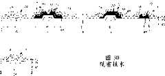
图1是示出使用现有技术的四掩模工艺制作的水平电场型液晶显示器的薄膜晶体管基板的结构的平面图。图2是沿图1中的线I-I′和线II-II′所截取的薄膜晶体管基板的剖面图。如图1和图2所示,薄膜晶体管基板包括彼此交叉地设置在下基板45上的选通线2和数据线4,在选通线2与数据线4之间设有栅绝缘膜46。薄膜晶体管6设在各交叉处附近。像素电极14和公共电极18设置在像素区域处,该像素区域由用于形成水平电场的选通线2和数据线4限定。公共线16与公共电极18连接。薄膜晶体管基板还包括一存储电容器20,其设置在像素电极14和公共线16之间的交叠部分处。此外,选通焊盘24与选通线2连接,数据焊盘30与数据线4连接,并且公共焊盘36与公共线16连接。选通线2向像素区域5提供选通信号,而数据线4向像素区域5提供数据信号。公共线16提供用于驱动液晶的基准电压,并且与位于像素区域5的一侧的选通线2相平行地设置在像素区域5的另一侧。FIG. 1 is a plan view showing the structure of a thin film transistor substrate of a horizontal electric field type liquid crystal display fabricated using a prior art four-mask process. FIG. 2 is a cross-sectional view of the thin film transistor substrate taken along line II' and line II-II' in FIG. 1 . As shown in FIGS. 1 and 2 , the TFT substrate includes gate lines 2 and data lines 4 intersecting each other on a
薄膜晶体管6响应于选通线2的选通信号,使得可以充入数据线4的像素信号并且将其保持在像素电极14上。薄膜晶体管6包括与选通线2连接的栅极8、与数据线4连接的源极10以及与像素电极14连接的漏极12。此外,薄膜晶体管6包括有源层48,其在源极10与漏极12之间限定一沟道。有源层48与栅极8上的栅绝缘膜46交叠。The
有源层48还与数据线4、下数据焊盘电极32以及上存储电极22交叠。在有源层48上设有用于与数据线4进行欧姆接触的欧姆接触层50。此外,在有源层48上还设有源极10、漏极12、下数据焊盘电极32以及上存储电极22。The
像素电极14通过穿过保护膜52的第一接触孔13连接到薄膜晶体管6的漏极12,并且被设置在像素区域5中。像素电极14包括:第一水平部分14A,与漏极12连接并且与相邻的选通线2平行地设置;第二水平部分14B,与公共线16交叠;以及指状部分14C,平行地设置在第一水平部分14A与第二水平部分14B之间。The
公共电极18与公共线16连接,并且设置在像素区域5中。具体地说,公共电极18与像素电极14的指状部分14C相平行地设置在像素区域5中。因此,可以在像素电极14(通过薄膜晶体管6向其提供像素信号)与公共电极18(通过公共线16向其提供基准电压)之间形成水平电场。因此,可以在像素电极14的指状部分14C与公共电极18之间形成水平电场。由于介电各向异性,通过这样的水平电场而在薄膜晶体管基板与滤色器基板之间沿水平方向排列的液晶分子发生旋转。根据液晶分子的旋转程度透过像素区域的光的透射率有所不同,从而实现灰度级。The
存储电容器20包括与公共线16和栅绝缘膜46交叠的上存储电极22、有源层48以及介于二者之间的欧姆接触层50。存储电容器20还包括一像素电极14,其通过设置在保护膜52中的第二接触孔21连接到上存储电极22。存储电容器20使得可以稳定地保持像素电极14上所充的像素信号,直到充入下一信号为止。The
选通线2通过选通焊盘24连接到选通驱动器(未示出)。选通焊盘24包括下选通焊盘电极26和上选通焊盘电极28,其中下选通焊盘电极26延伸自选通线2,上选通焊盘电极28通过穿过栅绝缘膜26和保护膜52的第三接触孔27连接到下选通焊盘电极26。数据线4通过数据焊盘30连接到数据驱动器(未示出)。数据焊盘30包括下数据焊盘电极32和上数据焊盘电极34,其中下数据焊盘电极32延伸自数据线4,上数据焊盘34通过穿过保护膜52的第四接触孔33连接到下数据焊盘电极32。公共线16通过公共焊盘36接收来自外部基准电压源(未示出)的基准电压。公共焊盘36包括下公共焊盘电极38和上公共焊盘电极40,其中下公共焊盘电极38延伸自公共线16,上公共焊盘电极40通过穿过栅绝缘膜46和保护膜52的第一接触孔39连接到下公共焊盘电极38。The gate line 2 is connected to a gate driver (not shown) through a
参照图3A至3D详细说明一种使用四道(four-round)掩模工艺来制造具有上述结构的薄膜晶体管基板的方法。参照图3A,通过第一掩模工艺在下基板45上提供一栅金属图案组,其包括选通线2、栅极8、下选通焊盘电极26、公共线16、公共电极18以及下公共焊盘电极38。Referring to FIGS. 3A to 3D , a method of manufacturing a thin film transistor substrate having the above structure using a four-round mask process will be described in detail. Referring to FIG. 3A, a gate metal pattern group is provided on the
通过以下步骤来形成该栅金属图案组。首先,利用诸如溅射的淀积技术在下基板45上形成一栅金属层。然后,利用第一掩模通过光刻法和刻蚀工艺对该栅金属层进行构图,从而形成包括选通线2、栅极8、下选通焊盘电极26、公共线16、公共电极18以及下公共焊盘电极38的所述栅金属图案组。所述栅金属层由诸如铝合金、铬(Cr)或者钼(Mo)的金属制成。The gate metal pattern group is formed through the following steps. First, a gate metal layer is formed on the
参照图3B,在设有栅金属图案组的下基板45上敷设栅绝缘膜46。此外,在栅绝缘膜46上通过第二掩模工艺提供半导体图案和源/漏金属图案组,其中,该半导体图案包括有源层48和欧姆接触层50,该源/漏金属图案组包括数据线4、源极10、漏极12、下数据焊盘电极32以及上存储电极22。更具体地说,通过适当的淀积技术(如等离子体增强化学气相淀积(PECVD))和/或溅射)在具有栅金属图案组的下基板45上顺序地设置栅绝缘膜46、非晶硅层、n+非晶硅层以及源/漏金属层。其中,栅绝缘膜46是由诸如氮化硅(SiNx)或氧化硅(SiOx)的无机绝缘材料制成的。所述源/漏金属层是由钼(Mo)、钛(Ti)、钽(Ta)或者钼合金制成的。Referring to FIG. 3B, a
然后,使用第二掩模通过光刻法在该源/漏金属层上形成光刻胶图案。在此情况下,使用具有与薄膜晶体管的沟道部分对应的衍射曝光部分的衍射曝光掩模作为第二掩模,从而使得沟道部分的光刻胶图案的高度低于其他图案部分。Then, a photoresist pattern is formed on the source/drain metal layer by photolithography using a second mask. In this case, a diffraction exposure mask having a diffraction exposure portion corresponding to the channel portion of the thin film transistor is used as the second mask so that the height of the resist pattern of the channel portion is lower than that of other pattern portions.
随后,使用光刻胶图案通过湿法刻蚀工艺对该源/漏金属层进行构图,从而限定包括数据线4、源极10、与源极10成为一体的漏极12以及上存储电极22的源/漏金属图案组。Subsequently, the source/drain metal layer is patterned by a wet etching process using a photoresist pattern, thereby defining a structure including the data line 4, the
接下来,通过灰化工艺将具有相对较低高度的光刻胶图案从沟道部分去除,随后通过干法刻蚀工艺对沟道部分的源/漏金属图案和欧姆接触层50进行刻蚀。由此,露出沟道部分的有源层48,以使源极10和漏极12分离。然后,通过剥离工艺去除残留在源/漏金属图案组上的光刻胶图案。Next, the photoresist pattern having a relatively low height is removed from the channel portion through an ashing process, and then the source/drain metal pattern and the
参照图3C,通过第三掩模工艺在栅绝缘膜46上形成包括第一至第五接触孔13、21、27、33和39的保护膜52。更具体地说,通过淀积技术(如等离子增强化学气相淀积(PECVD))在源/漏金属图案组的整个表面上淀积保护膜52。使用第三掩模通过光刻法和刻蚀工艺对保护膜52进行构图,以限定出第一至第五接触孔13、21、27、33和39。第一接触孔13穿过保护膜52,以露出漏极12。第二接触孔21穿过保护膜52,以露出上存储电极22。第三接触孔27穿过保护膜52和栅绝缘膜46,以露出下选通焊盘电极26。第四接触孔33穿过保护膜52以露出下数据焊盘电极32。第五接触孔39穿过保护膜52和栅绝缘膜46以露出下公共焊盘电极38。如果该源/漏金属层是由干法刻蚀率较高的金属(如钼(Mo))制成的,则第一接触孔13、第二接触孔21以及第四接触孔33将分别穿过漏极12、上存储电极22和下数据焊盘电极32从而露出这些电极的侧面。保护膜52由与栅绝缘膜46相同的无机材料制成,或者由具有较低介电常数的有机材料(例如丙稀酸有机化合物、BCB(苯并环丁烯)或者PFCB(全氟环丁烷))制成。Referring to FIG. 3C, a
参照图3D,通过第四掩模工艺在保护膜52上提供了透明导电膜图案组,其包括像素电极14、上选通焊盘电极28、上数据焊盘电极34以及上公共焊盘电极40。更具体地说,通过淀积技术(如溅射)将一透明导电膜敷设到保护膜52上。然后,使用第四掩模通过光刻法和刻蚀工艺对该透明导电膜进行构图,以形成包括像素电极14、上选通焊盘电极28、上数据焊盘电极34以及上公共焊盘电极40的透明导电图案组。像素电极14通过第一接触孔13与漏极12电连接,还通过第二接触孔21与上存储电极22电连接。上选通焊盘电极28通过第三接触孔27与下选通焊盘电极26电连接。上数据焊盘34通过第四接触孔33与下数据焊盘电极32电连接。上公共焊盘电极40通过第五接触孔39与下公共焊盘电极38电连接。透明导电膜由氧化铟锡(ITO)、氧化锡(TO)或者氧化铟锌(IZO)制成。Referring to FIG. 3D, a transparent conductive film pattern group including the
如上所述采用现有技术的水平电场型薄膜晶体管基板及基制造方法使用了四道掩模工艺,从而与使用五道掩模工艺的制造方法相比减少了制造工序数并由此降低了制造成本。然而,由于四道掩模工艺仍然是一种复杂的制造工艺,因此,成本降低有限。仍然存在简化制造工艺并且降低制造成本的需求。As mentioned above, the horizontal electric field type thin film transistor substrate and base manufacturing method of the prior art uses four masking processes, thereby reducing the number of manufacturing steps and thereby reducing the manufacturing process compared with the manufacturing method using five masking processes. cost. However, since the four-pass mask process is still a complex manufacturing process, cost reduction is limited. There is still a need to simplify the manufacturing process and reduce the manufacturing cost.
发明内容Contents of the invention
因此,本发明致力于提供一种利用水平电场的薄膜晶体管基板及其制造方法,其基本上消除了由于现有技术的限制和缺点所产生的一个或者更多个问题。Accordingly, the present invention is directed to providing a thin film transistor substrate utilizing a horizontal electric field and a method of fabricating the same that substantially obviate one or more problems due to limitations and disadvantages of the related art.
因此,本发明的一个目的是提供一种利用水平电场的薄膜晶体管基板及其制造方法,其具有简化的制造工艺。Accordingly, an object of the present invention is to provide a thin film transistor substrate using a horizontal electric field and a manufacturing method thereof, which have a simplified manufacturing process.
本发明的另一个目的是提供一种利用水平电场的薄膜晶体管基板及其制造方法,其具有改进的剥起(lift-off)工艺。Another object of the present invention is to provide a thin film transistor substrate using a horizontal electric field and a manufacturing method thereof, which have an improved lift-off process.
本发明的其他特征和优点将在随后的说明中阐明,部分从说明书中显见,或者可通过对本发明的实践而获知。通过文字说明及其权利要求书以及附图所具体指出的结构,可实现和获得本发明的其他目的和优点。Additional features and advantages of the invention will be set forth in the description which follows, and in part will be obvious from the description, or may be learned by practice of the invention. The other objectives and advantages of the invention will be realized and attained by the structure particularly pointed out in the written description and claims hereof as well as the appended drawings.
为实现这些和其他的优点并依据本发明的目的,如具体实现和广泛描述的,一种用于使用水平电场的薄膜晶体管基板结构包括:基板;由第一导电层形成在基板上且彼此平行的选通线和公共线;形成在基板、选通线和公共线上的栅绝缘膜;由第二导电层形成在栅绝缘膜上的数据线,其与选通线和公共线交叉,以限定像素区域;薄膜晶体管,与选通线和数据线相连接;保护膜,覆盖数据线和薄膜晶体管;由第三导电层形成并经由穿过保护膜和栅绝缘膜的孔与公共线相连接的公共电极,所述公共电极被布置在所述孔内;以及,由第二导电层形成的像素电极,其与薄膜晶体管相连接以在该像素电极与公共电极之间限定一水平电场。To achieve these and other advantages and in accordance with the purpose of the present invention, as embodied and broadly described, a thin film transistor substrate structure for using a horizontal electric field comprises: a substrate; a first conductive layer formed on the substrate parallel to each other The gate line and the common line; the gate insulating film formed on the substrate, the gate line and the common line; the data line formed on the gate insulating film by the second conductive layer, which crosses the gate line and the common line to Defining a pixel area; a thin film transistor connected to a gate line and a data line; a protective film covering the data line and the thin film transistor; formed of a third conductive layer and connected to a common line through a hole passing through the protective film and the gate insulating film a common electrode disposed in the hole; and a pixel electrode formed of the second conductive layer connected to the thin film transistor to define a horizontal electric field between the pixel electrode and the common electrode.
在另一方面,一种制造利用水平电场的薄膜晶体管基板结构的方法,包括以下步骤:通过对形成在基板上的第一导电层进行构图,形成选通线、与选通线相连接的栅极和下选通焊盘电极、以及与选通线平行的公共线以及与公共线相连接的下公共焊盘电极;在基板、选通线、栅极和公共线上敷设栅绝缘膜;在栅绝缘膜的一部分上形成半导体图案;通过对第二导电层进行构图,形成与选通线和公共线交叉以限定像素区域的数据线、与数据线相连接的源极和下数据焊盘电极,以及漏极,所述源极和漏极位于半导体图案上且彼此相对;在像素区域处形成与漏极相连接的像素电极;在像素电极、数据线、公共线、源极和漏极上敷设保护膜;对保护膜和栅绝缘膜进行构图,以在像素区域中提供一露出公共线的一部分的孔,并提供分别露出下选通焊盘电极、下公共焊盘电极和下数据焊盘电极的第一接触孔、第二接触孔和第三接触孔;以及,通过利用剥起工艺对第三导电层进行构图,形成公共电极、上选通焊盘电极、上公共焊盘电极和上数据焊盘电极,公共电极通过所述露出公共线的一部分的孔连接到公共线的所述露出的一部分,上选通焊盘电极位于第一接触孔内,上公共焊盘电极位于第二接触孔内,上数据焊盘电极位于第三接触孔内,其中,所述公共电极被布置在所述露出公共线的一部分的孔中,所述公共电极和所述像素电极被布置为限定一水平电场。In another aspect, a method of manufacturing a thin film transistor substrate structure utilizing a horizontal electric field includes the steps of: forming a gate line, a gate connected to the gate line, by patterning a first conductive layer formed on the substrate; Pole and lower gate pad electrodes, common lines parallel to the gate lines, and lower common pad electrodes connected to the common lines; laying a gate insulating film on the substrate, gate lines, gates, and common lines; A semiconductor pattern is formed on a part of the gate insulating film; by patterning the second conductive layer, a data line crossing the gate line and the common line to define a pixel area, a source electrode connected to the data line, and a lower data pad electrode are formed , and a drain electrode, the source electrode and the drain electrode are located on the semiconductor pattern and facing each other; a pixel electrode connected to the drain electrode is formed at the pixel region; on the pixel electrode, the data line, the common line, the source electrode and the drain electrode Laying a protective film; patterning the protective film and the gate insulating film to provide a hole exposing a part of the common line in the pixel region, and providing a lower gate pad electrode, a lower common pad electrode, and a lower data pad respectively exposed the first contact hole, the second contact hole and the third contact hole of the electrode; The data pad electrode, the common electrode is connected to the exposed part of the common line through the hole exposing a part of the common line, the upper gate pad electrode is located in the first contact hole, and the upper common pad electrode is located in the second contact In the hole, the upper data pad electrode is located in the third contact hole, wherein the common electrode is arranged in the hole exposing a part of the common line, and the common electrode and the pixel electrode are arranged to define a horizontal electric field.
在另一方面,一种制造利用水平电场的薄膜晶体管基板结构的方法,包括以下步骤:第一掩模工艺,用于通过对形成在基板上的第一导电层进行构图来形成选通线、与选通线相连接的栅极和下选通焊盘电极、与选通线平行的公共线以及与公共线相连接的下公共焊盘电极;在基板、选通线、栅极和公共线上敷设栅绝缘膜;第二掩模工艺,用于在栅绝缘膜的一部分上形成半导体图案,通过对第二导电层进行构图来形成与选通线和公共线交叉以限定像素区域的数据线、与数据线相连接的源极和下数据焊盘电极、以及漏极,并且在像素区域处形成与漏极相连接的像素电极,所述源极和漏极位于半导体图案上且彼此相对;在像素电极、数据线、公共线、源极和漏极上敷设保护膜;以及第三掩模工艺,对保护膜和栅绝缘膜进行构图以在像素区域中提供露出公共线的一部分的孔,并提供分别露出下选通焊盘电极、下公共焊盘电极和下数据焊盘电极的第一接触孔、第二接触孔和第三接触孔,并且通过利用剥起工艺对第三导电层进行构图,形成公共电极、上选通焊盘电极、上公共焊盘电极和上数据焊盘电极,公共电极通过所述露出公共线的一部分的孔连接到公共线的所述露出的一部分,上选通焊盘电极位于第一接触孔内,上公共焊盘电极位于第二接触孔内,上数据焊盘电极位于第三接触孔内,其中,所述公共电极被布置在所述露出公共线的一部分的孔中,所述公共电极和所述像素电极被布置为限定一水平电场。In another aspect, a method of manufacturing a thin film transistor substrate structure using a horizontal electric field includes the steps of: a first mask process for forming a gate line by patterning a first conductive layer formed on the substrate, gate and lower gate pad electrodes connected to the gate lines, common lines parallel to the gate lines, and lower common pad electrodes connected to the common lines; laying a gate insulating film thereon; a second mask process for forming a semiconductor pattern on a part of the gate insulating film, and forming a data line crossing the gate line and the common line to define a pixel area by patterning the second conductive layer , a source electrode connected to the data line, a lower data pad electrode, and a drain electrode, and a pixel electrode connected to the drain electrode is formed at the pixel region, the source electrode and the drain electrode are located on the semiconductor pattern and face each other; laying a protective film on the pixel electrodes, data lines, common lines, source electrodes, and drain electrodes; and a third mask process of patterning the protective film and the gate insulating film to provide a hole exposing a part of the common line in the pixel region, And provide the first contact hole, the second contact hole and the third contact hole respectively exposing the lower gate pad electrode, the lower common pad electrode and the lower data pad electrode, and carry out the third conductive layer by using the lift-off process Patterning to form a common electrode, an upper gate pad electrode, an upper common pad electrode and an upper data pad electrode, the common electrode is connected to the exposed part of the common line through the hole that exposes a part of the common line, and the upper selection The through pad electrode is located in the first contact hole, the upper common pad electrode is located in the second contact hole, and the upper data pad electrode is located in the third contact hole, wherein the common electrode is arranged on the exposed common line In a portion of the aperture, the common electrode and the pixel electrode are arranged to define a horizontal electric field.
应该理解,上述总体说明和以下的详细说明都是示例性和说明性的,旨在提供对所要求保护的本发明的进一步解释。It is to be understood that both the foregoing general description and the following detailed description are exemplary and explanatory and are intended to provide further explanation of the invention as claimed.
附图说明Description of drawings
所包括的附图用于提供对本发明的进一步理解,其被并入说明书中并构成说明书的一部分。附图示出了本发明的实施例,并与说明书一起用于解释本发明的原理。The accompanying drawings are included to provide a further understanding of the invention, and are incorporated in and constitute a part of this specification. The drawings illustrate the embodiments of the invention and together with the description serve to explain the principles of the invention.
图1是示出一种采用现有技术的利用水平电场的液晶显示器件的薄膜晶体管的结构的平面图;1 is a plan view showing the structure of a thin film transistor of a liquid crystal display device using a prior art using a horizontal electric field;
图2是沿图1中的线I-I′和II-II′所截取的薄膜晶体管基板的剖面图;Fig. 2 is the cross-sectional view of the TFT substrate taken along the lines I-I' and II-II' in Fig. 1;
图3A至3D是示出图2中所示的薄膜晶体管基板的制造方法的剖面图;3A to 3D are cross-sectional views illustrating a method of manufacturing the thin film transistor substrate shown in FIG. 2;
图4是示出根据本发明的一示意性实施例的水平电场型薄膜晶体管基板的结构的平面图;4 is a plan view showing the structure of a horizontal electric field type thin film transistor substrate according to an exemplary embodiment of the present invention;
图5是沿图4中的线III-III′、IV-IV′、V-V′、VI-VI′以及VII-VII′所截取的薄膜晶体管基板的剖面图;5 is a sectional view of the thin film transistor substrate taken along lines III-III', IV-IV', V-V', VI-VI' and VII-VII' in FIG. 4;
图6A和图6B分别是用于对根据本发明的示例性实施例的薄膜晶体管基板的制造方法中的第一掩模工艺进行说明的平面图和剖面图;6A and 6B are a plan view and a cross-sectional view, respectively, for explaining a first mask process in a method of manufacturing a thin film transistor substrate according to an exemplary embodiment of the present invention;
图7A和图7B分别是用于对根据本发明的示例性实施例的薄膜晶体管基板的制造方法中的第二掩模工艺进行说明的平面图和剖面图;7A and 7B are a plan view and a cross-sectional view, respectively, for explaining a second mask process in a method of manufacturing a thin film transistor substrate according to an exemplary embodiment of the present invention;
图8A至图8D是用于对根据本发明的示例性实施例的薄膜晶体管基板的制造方法中的第二掩模工艺进行具体说明的剖面图;8A to 8D are cross-sectional views for specifically describing a second mask process in a method of manufacturing a thin film transistor substrate according to an exemplary embodiment of the present invention;
图9A和图9B分别是用于对根据本发明的示例性实施例的薄膜晶体管基板的制造方法中的第三掩模工艺进行说明的平面图和剖面图;以及9A and 9B are a plan view and a cross-sectional view, respectively, for explaining a third mask process in a method of manufacturing a thin film transistor substrate according to an exemplary embodiment of the present invention; and
图10A至图10D是用于对根据本发明的示例性实施例的薄膜晶体管基板的制造方法中的第三掩模工艺进行具体说明的剖面图。10A to 10D are cross-sectional views for specifically explaining a third mask process in a method of manufacturing a thin film transistor substrate according to an exemplary embodiment of the present invention.
具体实施方式Detailed ways
下面参照附图详细说明本发明的优选实施例,其示例在附图中示出。Preferred embodiments of the invention will be described in detail below with reference to the accompanying drawings, examples of which are shown.
以下,将参照图4至图10D对本发明的示例性实施例进行详细说明。图4是示出根据本发明实施例的利用水平电场的薄膜晶体管基板的结构的平面图。图5是沿图4的线III-III′、IV-IV′、V-V′、VI-VI′以及VII-VII′所截取的薄膜晶体管基板的剖面图。Hereinafter, an exemplary embodiment of the present invention will be described in detail with reference to FIGS. 4 to 10D. 4 is a plan view illustrating the structure of a thin film transistor substrate using a horizontal electric field according to an embodiment of the present invention. 5 is a cross-sectional view of the thin film transistor substrate taken along lines III-III', IV-IV', V-V', VI-VI', and VII-VII' of FIG. 4 .
参照图4和图5,该薄膜晶体管基板包括:彼此交叉地设置在下基板145上选通线102和数据线104,其间设有栅绝缘膜146;设置在各交叉处的薄膜晶体管106;像素电极114和公共电极118,设置在由交叉点所限定的像素区域处,用于形成水平电场;以及,连接到公共电极118的公共线116。此外,薄膜晶体管基板包括存储电容器120、与选通线102连接的选通焊盘125、与数据线104连接的数据焊盘131,以及与公共线116连接的公共焊盘135,其中存储电容器120设置在前级(pre-stage)选通线102、公共线116、公共电极118和上存储电极122之间的交叠部分处。Referring to FIG. 4 and FIG. 5, the thin film transistor substrate includes: the
被提供选通信号的选通线102和被提供数据信号的数据线104彼此交叉以限定像素区域。其中,选通线102由第一导电层(即,栅金属层)形成,而数据线104由第二导电层(即,源/漏金属层)形成。
薄膜晶体管106响应于选通线102的选通信号,使得能够充入数据线104的像素信号并且将其保持在像素电极114中。为此,薄膜晶体管106包括:与选通线102连接的栅极108;与数据线104连接的源极110;与源极110相对的漏极112;与栅极108交叠的有源层148,栅绝缘膜146位于两者之间,以在源极110与漏极112之间限定一沟道;以及,欧姆接触层150,设置在不包括沟道的有源层148上,以实现与源极10和漏极112的欧姆接触。The
此外,有源层148及欧姆接触层150与数据线104、下数据焊盘电极130以及上存储电极122交叠,数据线104、下数据焊盘电极130以及上存储电极122与源极110和漏极112一起由第二导电层形成。In addition, the
公共线116和公共电极118提供一用于驱动液晶材料的基准电压。公共线116包括第一公共线116A和第二公共线116B,第一公共线116A被设置为在显示区域中与选通线102一起横跨像素区域,而第二公共线116B在非显示区域中公共地连接多条第一公共线116A。公共线116与选通线102一起由第一导电层(或者栅金属层)形成。The
公共电极118连接到第一公共线116A,并被形成为位于像素区域的指状,以与像素电极114相平行。更具体地说,公共电极118包括邻近选通线并与其平行的横向部分118A,以及从横向部分118A延伸进入像素区域并且与像素电极114部分平行的指状部分118B。公共电极118由位于限定在像素区域中的公共电极孔164内部的第三导电层(即,透明层或钛)形成。将公共电极孔164形成为穿过保护膜152和栅绝缘膜146。公共电极孔164露出第一公共线116A的与公共电极118的指状部分118B交叠的部分,从而将公共电极118连接到第一公共线116A。其中,如果将诸如钛(Ti)的不透明金属用作第三导电层,则可以防止在像素区域中通过公共电极118的漏光。The
像素电极114与薄膜晶体管106的漏极112连接,并且与公共电极118一起在像素区域中形成水平电场。为此,像素电极114包括横向部分114A和指状部分114B,其中该横向部分114A与选通线102平行设置并且与漏极112相连接,该指状部分114B从横向部分114A延伸进入像素区域,并且与公共电极118的指状部分118B相平行。像素电极114与数据线104、源极110和漏极112一起由第二导电层形成。由此,在像素电极114(通过薄膜晶体管106和公共电极118对其提供像素信号)与第二公共线116B(通过公共线116对其提供基准电压)之间形成了水平电场。由于介电各向异性,通过水平电场而在薄膜晶体管基板与滤色器基板之间沿水平方向排列的液晶分子发生旋转。根据液晶分子的旋转程度,透过像素区域的光的透射率有所不同,从而实现灰度级。The
存储电容器120包括:第一公共线116A的用作第一下存储电极的一部分,以及与第一公共线116A的一部分交叠的上存储电极122,在上存储电极122与第一公共线116A的一部分之间设有栅绝缘膜146、有源层148以及欧姆接触层150。其中,上存储电极122连接在像素电极114的与第一公共线116A交叉的指状部分114B之间,并且与像素电极114一起由第二导电层形成。存储电容器120使得可以稳定地保持充入像素电极114中的像素信号,直到充入下一像素信号为止。The
选通线102通过选通焊盘125连接到选通驱动器(未示出)。选通焊盘125包括下选通焊盘电极124和上选通焊盘电极128,其中下选通焊盘电极124延伸自选通线102,上选通焊盘电极128经由穿过栅绝缘膜146和保护膜152的第一接触孔166连接到下选通焊盘电极124。The
公共线116通过公共焊盘135接收来自外部基准电压源(未示出)的基准电压。公共焊盘135包括下公共焊盘电极136和上公共焊盘电极140,其中下公共焊盘电极136延伸自公共线116,上公共焊盘电极140经由穿过栅绝缘膜146和保护膜152的第二接触孔170连接到下公共焊盘电极136。The
数据线104通过数据焊盘131连接到数据驱动器(未示出)。数据焊盘131包括下数据焊盘电极130和上数据焊盘电极134,其中下数据焊盘电极130延伸自数据线104,上数据焊盘134通过穿过保护膜152的第三接触孔168连接到下数据焊盘电极130。The
在该薄膜晶体管基板中,上选通焊盘电极128、上数据焊盘电极134以及上公共焊盘电极140与公共电极114一起由第三导电层形成。通过剥起工艺对第三导电层进行构图,以去除用于对保护膜152和栅绝缘膜146进行构图的光刻胶图案。由此,所构图的第三导电层形成与保护膜153的分界面。通过采用剥起工艺,根据本发明示意性实施例的薄膜晶体管基板可以去掉用于对第三导电层进行构图的一道掩模工艺。在此情况下,将公共电极孔164与第一至第三接触孔166、170及168一起用作剥离剂渗透路径(stripper penetration path),从而加强了光刻胶图案的剥离能力。In the thin film transistor substrate, the upper
以下将详细说明根据本发明示意性实施例的具有上述优点的薄膜晶体管基板的制造方法。The manufacturing method of the thin film transistor substrate having the above-mentioned advantages according to the exemplary embodiment of the present invention will be described in detail below.
图6A和图6B分别是用于对根据本发明示意性实施例的利用水平电场的薄膜晶体管基板的制造方法中的第一掩模工艺进行说明的平面图和剖面图。6A and 6B are a plan view and a cross-sectional view, respectively, for explaining a first mask process in a method of manufacturing a thin film transistor substrate using a horizontal electric field according to an exemplary embodiment of the present invention.
如图6A和图6B所示,通过第一掩模工艺在下基板145上设置第一导电图案组,其包括选通线102、栅极108、下选通焊盘电极124、公共线116以及下公共焊盘电极136。更具体地说,通过诸如溅射的淀积技术,在下基板145上形成第一导电层。然后,利用第一掩模通过光刻和刻蚀对第一导电层进行构图,从而形成包括选通线102、栅极108、下选通焊盘电极124、公共线116以及下公共焊盘电极136的第一导电图案组。其中所述第一导电层由Cr、MoW、Cr/Al、Cu、Al(Nd)、Mo/Al、Mo/Al(Nd)、Cr/Al(Nd)或者其他适当的材料制成。As shown in FIG. 6A and FIG. 6B, a first conductive pattern group is provided on the
图7A和图7B是用于对根据本发明示例性实施例的利用水平电场的薄膜晶体管基板的制造方法中的第二掩模工艺进行说明的示意性的平面图和剖面图。图8A至图8D是用于具体说明该第二掩模工艺的剖面图。7A and 7B are schematic plan and cross-sectional views for explaining a second mask process in a method of manufacturing a thin film transistor substrate using a horizontal electric field according to an exemplary embodiment of the present invention. 8A to 8D are cross-sectional views for specifically explaining the second mask process.
首先,通过诸如等离子体增强化学气相淀积(PECVD))、溅射等淀积技术,在设有第一导电图案组的下基板145上形成栅绝缘膜146。其中,栅绝缘膜146由诸如硅氮化物(SiNx)或硅氧化物(SiOx)的无机绝缘材料制成。First, a
如图7A至图7B所示,在栅绝缘膜146上设置一包括有源层148和欧姆接触层150的半导体图案;并且通过第二掩模工艺设置一第二导电图案组,其包括数据线104、源极110、漏极112、像素电极114、下数据焊盘电极130以及上存储电极122。其中,像素电极114由不透明的第二导电层制成,从而防止由其引起的漏光。As shown in FIGS. 7A to 7B, a semiconductor pattern including an
更具体地说,如图8A所示,通过淀积技术(如等离子体增强化学气相淀积(PECVD)、溅射等等)在栅绝缘膜146上顺序地形成非晶硅层148A、n+非晶硅层150A以及第二导电层156。其中,第二导电层由Cr、MoW、Cr/Al、Cu、Al(Nd)、Mo/Al、Mo/Al(Nd)、Cr/Al(Nd)或者其他适当的材料制成。More specifically, as shown in FIG. 8A, an
然后,在第二导电层156上完全地敷设光刻胶膜,然后使用第二掩模(其为部分曝光掩模)通过光刻,在第二导电层156上形成如图8A所示的具有台阶覆盖(step coverage)的光刻胶图案158。在此情况下,使用在将要形成薄膜晶体管的沟道的部分处具有一衍射曝光部分(或半透射部分或者透射反射部分)的部分曝光掩模作为第二掩模。由此,相比与第二掩模的透射部分(或遮挡部分)对应的光刻胶图案158,与第二掩模的衍射曝光部分(或半透射部分)对应的光刻胶图案158具有更低的高度。换言之,与位于其他源/漏金属图案组部分的光刻胶158相比,位于沟道部分的光刻胶图案158具有更低的高度。Then, a photoresist film is completely laid on the second
随后,使用光刻胶图案158通过湿法刻蚀工艺对第二导电层156进行构图。由此,如图8B所示形成第二导电图案组,其包括数据线104、从数据线104伸出的源极110、与源极110形成为一体的漏极112、与漏极112形成为一体的像素电极114、延伸自数据线104的下数据焊盘电极130,以及与像素电极114形成为一体的上存储电极122。其中上存储电极122连接在与第一公共线116A交叠的像素电极114的指状部分114B之间。此外,使用同一光刻胶图案158通过干法刻蚀工艺,同时对n+非晶硅层150A和非晶硅层148A进行构图,从而提供这样一种结构,其中如图8B所示沿着第二导电图案组形成有欧姆接触层150和有源层148。Subsequently, the second
接下来,如图8C所示,通过使用氧气(O2)的灰化处理来去除位于沟道部分的具有相对较低高度的光刻胶图案158,而位于其他的第二导电图案组部分处的光刻胶图案158具有较低的高度。使用以此方式所残留的光刻胶图案158通过干法刻蚀工艺,如图8C所示从形成有沟道的部分对第二导电层和欧姆接触层150进行刻蚀,从而使源极110与漏极112断开并露出有源层148。由此,在源极110与漏极112之间形成一由有源层148所构成的沟道。Next, as shown in FIG. 8C, the
然后,如图8D所示,通过剥离工艺将残留在第二导电图案组部分上的光刻胶图案158完全去除。Then, as shown in FIG. 8D , the
图9A和图9B分别是用于对根据本发明示例性实施例的使用水平电场的薄膜晶体管基板的制造方法中的第三掩模工艺进行说明的平面图和剖面图。图10A至图10D是用于对该第三掩模工艺进行具体说明的剖面图。9A and 9B are a plan view and a cross-sectional view, respectively, for explaining a third mask process in a method of manufacturing a thin film transistor substrate using a horizontal electric field according to an exemplary embodiment of the present invention. 10A to 10D are cross-sectional views for specifically describing the third mask process.
如图9A和图9B所示,通过第三掩模工艺对保护膜152和栅绝缘膜146进行构图。由此形成包括公共电极118、上选通焊盘电极128、上数据焊盘电极134以及上公共焊盘电极140的第三导电图案组。该第三导电图案组与经构图的保护膜152相接,而无任何交叠部分。As shown in FIGS. 9A and 9B , the
更具体地说,如图10A所示,在设有第二导电图案组的栅绝缘膜146上完全地形成保护膜152。其中,保护膜152由与栅绝缘膜146相似的无机绝缘材料或有机绝缘材料制成。此外,使用第三掩模通过光刻在如图10A所示必须存有保护膜152的部分处形成光刻胶图案160。More specifically, as shown in FIG. 10A, the
接下来,使用光刻胶图案160通过干法刻蚀对保护膜152和栅绝缘膜146进行构图,从而形成穿过保护膜152(或者保护膜152和栅绝缘膜146)的公共电极孔164、第一至第三接触孔166、170及168。其中,公共电极孔164在将要形成公共电极的部分处穿过保护膜152和栅绝缘膜146,从而露出第一公共线116A的一部分。此外,第一至第三接触孔166、170及168分别露出下选通焊盘电极124、下公共焊盘电极136以及下数据焊盘电极130。Next, the
随后,通过诸如溅射等的淀积技术,在如图10C所示存有光刻胶图案160的薄膜晶体管基板上完全地形成第三导电层172。第三导电层172由包含氧化铟锡(ITO)、氧化锡(TO)、氧化铟锌(IZO)或者SnO2等的透明导电膜制成。另选地,第三导电膜172由具有高抗蚀性和高强度的金属层(如钛(Ti)或钨(W))制成。Subsequently, the third
通过剥起工艺将光刻胶图案160和其上的第三导电层172一起去除,从而对第三导电层172进行构图。由此,如图10D所示,在公共电极孔164、第一至第三接触孔166、170及168处分别设置了公共电极118、上选通焊盘电极128、上公共焊盘电极140以及上数据焊盘电极134。The
在此情况下,将公共电极孔164和第一至第三接触孔166、170及168设置在不存在光刻胶图案160的部分处,作为剥离剂渗透路径,以使更大量的剥离剂A可以渗入光刻胶图案160与保护膜152之间的分界部分。结果,利用剥离剂A可以容易地使覆盖有第三导电层172的光刻胶图案160与保护膜152分离。由于对保护膜152的过刻蚀,使得与位于设有公共电极孔164和第一至第三接触孔166、170及168的部分处的保护膜152的边沿相比,光刻胶图案160的边沿具有更加突出的形状(未示出),从而实现了更加容易的分离。此外,由于以线性淀积在光刻胶图案160的边沿与保护膜152的边沿之间的第三导电层172是开口的,或者利用光刻胶图案160的突出边缘使第三导电层172淀积得相对较薄,从而使剥离剂可容易地渗入,所以实现了更加容易的分离。In this case, the
如上所述,通过剥起工艺将第三导电层172的不必要的部分连同光刻胶图案160一起去除,从而提供了与保护膜152形成分界面的第三导电图案组。更具体地说,在公共电极孔164中设置了公共电极118,以与所露出的第一公共线116A相连接。在对应的接触孔166、170和168中分别设置了上选通焊盘电极128、上公共焊盘电极140以及上数据焊盘电极134,以连接到下选通焊盘电极124、下公共焊盘电极136以及下数据焊盘电极130。As described above, unnecessary portions of the third
其中,如果使用钛(Ti)作为第三导电层172,则可以防止透过公共电极118和像素电极114的漏光。此外,可以防止对焊盘部分的电化学侵蚀、撕裂等。由此可以确保可靠性。Wherein, if titanium (Ti) is used as the third
如上所述,根据本发明,采用剥起工艺来减少用于第三导电层的掩模工艺。因此,通过三道掩模工艺制造了薄膜晶体管基板,从而可以简化制造过程,以降低制造成本并且提高产品合格率。此外,根据本发明,使用穿过保护膜的公共电极孔、第一至第三接触孔作为剥离剂渗透路径,从而有效地提高了覆盖有第三导电层的光刻胶图案的剥离能力。As described above, according to the present invention, the lift-off process is used to reduce the mask process for the third conductive layer. Therefore, the thin film transistor substrate is manufactured through three mask processes, so that the manufacturing process can be simplified, so as to reduce the manufacturing cost and improve the yield of products. In addition, according to the present invention, the common electrode hole passing through the protective film, the first to third contact holes are used as the stripping agent penetration path, thereby effectively improving the stripping ability of the photoresist pattern covered with the third conductive layer.
本领域技术人员应该清楚,可以在不脱离本发明的实质或范围的情况下,对本发明的使用水平电场的薄膜晶体管基板及基制造方法进行多种修改和变型。因此,本发明将覆盖落入所附权利要求书及其等同物的范围内的对本发明的修改和变型。It should be apparent to those skilled in the art that various modifications and variations can be made to the thin film transistor substrate using a horizontal electric field and the base manufacturing method of the present invention without departing from the spirit or scope of the present invention. Thus, it is intended that the present invention covers the modifications and variations of this invention that come within the scope of the appended claims and their equivalents.
Claims (21)
Translated fromChineseApplications Claiming Priority (3)
| Application Number | Priority Date | Filing Date | Title |
|---|---|---|---|
| KR1020030077661AKR100560403B1 (en) | 2003-11-04 | 2003-11-04 | Horizontal field applied thin film transistor substrate and manufacturing method thereof |
| KR1020030077661 | 2003-11-04 | ||
| KR10-2003-0077661 | 2003-11-04 |
Publications (2)
| Publication Number | Publication Date |
|---|---|
| CN1614492A CN1614492A (en) | 2005-05-11 |
| CN100345053Ctrue CN100345053C (en) | 2007-10-24 |
Family
ID=34545739
Family Applications (1)
| Application Number | Title | Priority Date | Filing Date |
|---|---|---|---|
| CNB2004100925352AExpired - Fee RelatedCN100345053C (en) | 2003-11-04 | 2004-11-04 | Thin film transistor substrate using a horizontal electric field and fabricating method thereof |
Country Status (3)
| Country | Link |
|---|---|
| US (2) | US7132688B2 (en) |
| KR (1) | KR100560403B1 (en) |
| CN (1) | CN100345053C (en) |
Families Citing this family (17)
| Publication number | Priority date | Publication date | Assignee | Title |
|---|---|---|---|---|
| KR100560404B1 (en)* | 2003-11-04 | 2006-03-14 | 엘지.필립스 엘시디 주식회사 | Horizontal field applied thin film transistor substrate and manufacturing method thereof |
| KR100560402B1 (en)* | 2003-11-04 | 2006-03-14 | 엘지.필립스 엘시디 주식회사 | Horizontal field applied thin film transistor substrate and manufacturing method thereof |
| KR100764903B1 (en)* | 2004-09-07 | 2007-10-09 | 김병두 | Pulverized coal boiler furnace structure for power plant |
| KR101201017B1 (en)* | 2005-06-27 | 2012-11-13 | 엘지디스플레이 주식회사 | Liquid crystal display and fabricating method thereof |
| KR101225440B1 (en)* | 2005-06-30 | 2013-01-25 | 엘지디스플레이 주식회사 | Liquid crystal display and fabricating method thereof |
| US8212953B2 (en)* | 2005-12-26 | 2012-07-03 | Semiconductor Energy Laboratory Co., Ltd. | Semiconductor device and method for manufacturing the same |
| TWI294177B (en)* | 2005-12-30 | 2008-03-01 | Au Optronics Corp | Method for manufacturing pixel structure |
| JP4404881B2 (en)* | 2006-08-09 | 2010-01-27 | 日本電気株式会社 | Thin film transistor array, manufacturing method thereof, and liquid crystal display device |
| KR100920483B1 (en)* | 2007-07-20 | 2009-10-08 | 엘지디스플레이 주식회사 | Array substrate for liquid crystal display device and manufacturing method thereof |
| KR101473839B1 (en)* | 2007-10-17 | 2014-12-18 | 엘지디스플레이 주식회사 | In plane switching mode liquid crystal display device and method of fabricating the same |
| KR101686094B1 (en)* | 2009-12-31 | 2016-12-13 | 엘지디스플레이 주식회사 | Liquid Crystal Display Device and Method for Manufacturing the Same |
| KR101274719B1 (en)* | 2010-06-11 | 2013-06-25 | 엘지디스플레이 주식회사 | Thin film transistor substrate, method of fabricating the same, and flat display having the same |
| US9048256B2 (en)* | 2012-11-16 | 2015-06-02 | Apple Inc. | Gate insulator uniformity |
| DE102013002079A1 (en) | 2013-02-06 | 2014-08-07 | Volvo Construction Equipment Germany GmbH | Construction machinery |
| CN103887236B (en)* | 2014-03-17 | 2016-08-24 | 京东方科技集团股份有限公司 | Array base palte and manufacture method, display device |
| CN103972243B (en)* | 2014-04-24 | 2017-03-29 | 京东方科技集团股份有限公司 | A kind of array base palte and preparation method thereof, display device |
| CN114868077B (en)* | 2020-10-28 | 2023-09-19 | 京东方科技集团股份有限公司 | Driving backboard, manufacturing method thereof and display module |
Citations (5)
| Publication number | Priority date | Publication date | Assignee | Title |
|---|---|---|---|---|
| JPH09101538A (en)* | 1995-10-04 | 1997-04-15 | Hitachi Ltd | Active matrix type liquid crystal display device and manufacturing method thereof |
| CN1188244A (en)* | 1996-05-01 | 1998-07-22 | 斯坦利电气株式会社 | Liquid crystal display of horizontal field type |
| EP1008896A1 (en)* | 1997-04-11 | 2000-06-14 | Hitachi, Ltd. | Liquid crystal display device |
| CN1403855A (en)* | 2001-08-30 | 2003-03-19 | 株式会社日立制作所 | Liquid crystal display with high-response IPS display mode |
| US20030122990A1 (en)* | 2001-12-31 | 2003-07-03 | Kim Ik Soo | Array substrate for in-plane switching mode liquid crystal display device and method of fabricating the same |
Family Cites Families (6)
| Publication number | Priority date | Publication date | Assignee | Title |
|---|---|---|---|---|
| US6337726B1 (en)* | 1998-02-24 | 2002-01-08 | Kabushiki Kaisha Toshiba | Array substrate for liquid crystal display element |
| JP2001183666A (en)* | 1999-12-24 | 2001-07-06 | Nec Corp | Liquid crystal display device |
| KR100773876B1 (en) | 2001-12-28 | 2007-11-06 | 엘지.필립스 엘시디 주식회사 | Array board for transverse electric field type liquid crystal display device and manufacturing method thereof |
| KR100494703B1 (en) | 2001-12-31 | 2005-06-13 | 비오이 하이디스 테크놀로지 주식회사 | A method for manufacturing of thin film transistor liquid crystal display |
| KR100560401B1 (en)* | 2003-11-04 | 2006-03-14 | 엘지.필립스 엘시디 주식회사 | Horizontal field applied thin film transistor substrate and manufacturing method thereof |
| KR100566816B1 (en)* | 2003-11-04 | 2006-04-03 | 엘지.필립스 엘시디 주식회사 | Horizontal field applied thin film transistor substrate and manufacturing method thereof |
- 2003
- 2003-11-04KRKR1020030077661Apatent/KR100560403B1/ennot_activeExpired - Fee Related
- 2004
- 2004-11-02USUS10/978,522patent/US7132688B2/ennot_activeExpired - Lifetime
- 2004-11-04CNCNB2004100925352Apatent/CN100345053C/ennot_activeExpired - Fee Related
- 2006
- 2006-10-10USUS11/544,748patent/US7446337B2/ennot_activeExpired - Lifetime
Patent Citations (5)
| Publication number | Priority date | Publication date | Assignee | Title |
|---|---|---|---|---|
| JPH09101538A (en)* | 1995-10-04 | 1997-04-15 | Hitachi Ltd | Active matrix type liquid crystal display device and manufacturing method thereof |
| CN1188244A (en)* | 1996-05-01 | 1998-07-22 | 斯坦利电气株式会社 | Liquid crystal display of horizontal field type |
| EP1008896A1 (en)* | 1997-04-11 | 2000-06-14 | Hitachi, Ltd. | Liquid crystal display device |
| CN1403855A (en)* | 2001-08-30 | 2003-03-19 | 株式会社日立制作所 | Liquid crystal display with high-response IPS display mode |
| US20030122990A1 (en)* | 2001-12-31 | 2003-07-03 | Kim Ik Soo | Array substrate for in-plane switching mode liquid crystal display device and method of fabricating the same |
Also Published As
| Publication number | Publication date |
|---|---|
| KR20050042993A (en) | 2005-05-11 |
| CN1614492A (en) | 2005-05-11 |
| US7446337B2 (en) | 2008-11-04 |
| US20050092990A1 (en) | 2005-05-05 |
| US20070029551A1 (en) | 2007-02-08 |
| KR100560403B1 (en) | 2006-03-14 |
| US7132688B2 (en) | 2006-11-07 |
Similar Documents
| Publication | Publication Date | Title |
|---|---|---|
| CN100447645C (en) | Thin film transistor substrate of horizontal electric field type liquid crystal display device and manufacturing method thereof | |
| US7599034B2 (en) | Thin film transistor substrate of a horizontal electric field type LCD and fabricating method thereof | |
| CN100345053C (en) | Thin film transistor substrate using a horizontal electric field and fabricating method thereof | |
| CN100538999C (en) | Adopt the thin film transistor base plate and the manufacture method thereof of horizontal component of electric field | |
| CN1514468A (en) | Thin film transistor array substrate and manufacturing method thereof | |
| CN1892394A (en) | Liquid crystal display device and fabricating method thereof | |
| CN1797157A (en) | Liquid crystal display device and fabricating method thereof | |
| US7428032B2 (en) | Horizontal electric field LCD TFT substrate having gate insulating layer of varying thickness and fabricating method thereof | |
| CN1614489A (en) | Thin film transistor substrate for horizontal electric field LCD device and its manufacture | |
| JP4499628B2 (en) | Liquid crystal display device and manufacturing method thereof | |
| JP4392390B2 (en) | Liquid crystal display device and manufacturing method thereof | |
| CN1614486A (en) | Liquid crystal display of horizontal electronic field applying type and fabricating method thereof | |
| KR100499376B1 (en) | Thin film transistor array substrate and manufacturing method of the same | |
| CN100335960C (en) | Thin film transistor array substrate and fabricating method thereof | |
| KR100538327B1 (en) | Thin film transistor array substrate of horizontal electronic field applying type and fabricating method thereof | |
| US7388226B2 (en) | Liquid crystal display of horizontal electronic field applying type and fabricated method thereof | |
| KR100504572B1 (en) | Liquid crystal display apparatus of horizontal electric field applying type and fabricating method thereof | |
| KR100600088B1 (en) | Horizontal field applied liquid crystal display device and manufacturing method thereof | |
| KR101329447B1 (en) | Thin film transistor array substrate and manufacturing method of the same |
Legal Events
| Date | Code | Title | Description |
|---|---|---|---|
| C06 | Publication | ||
| PB01 | Publication | ||
| C10 | Entry into substantive examination | ||
| SE01 | Entry into force of request for substantive examination | ||
| C14 | Grant of patent or utility model | ||
| GR01 | Patent grant | ||
| C56 | Change in the name or address of the patentee | Owner name:LG DISPLAY CO., LTD. Free format text:FORMER NAME OR ADDRESS: LG. PHILIP LCD CO., LTD. | |
| CP01 | Change in the name or title of a patent holder | Address after:Seoul, South Kerean Patentee after:LG Display Co., Ltd. Address before:Seoul, South Kerean Patentee before:LG Philips LCD Co., Ltd. | |
| CF01 | Termination of patent right due to non-payment of annual fee | ||
| CF01 | Termination of patent right due to non-payment of annual fee | Granted publication date:20071024 Termination date:20171104 |