CN100342539C - Semiconductor device and mfg. method thereof - Google Patents
Semiconductor device and mfg. method thereofDownload PDFInfo
- Publication number
- CN100342539C CN100342539CCNB021495181ACN02149518ACN100342539CCN 100342539 CCN100342539 CCN 100342539CCN B021495181 ACNB021495181 ACN B021495181ACN 02149518 ACN02149518 ACN 02149518ACN 100342539 CCN100342539 CCN 100342539C
- Authority
- CN
- China
- Prior art keywords
- mentioned
- layer
- soi
- support substrate
- semiconductor device
- Prior art date
- Legal status (The legal status is an assumption and is not a legal conclusion. Google has not performed a legal analysis and makes no representation as to the accuracy of the status listed.)
- Expired - Fee Related
Links
Images


Classifications
- H—ELECTRICITY
- H10—SEMICONDUCTOR DEVICES; ELECTRIC SOLID-STATE DEVICES NOT OTHERWISE PROVIDED FOR
- H10D—INORGANIC ELECTRIC SEMICONDUCTOR DEVICES
- H10D86/00—Integrated devices formed in or on insulating or conducting substrates, e.g. formed in silicon-on-insulator [SOI] substrates or on stainless steel or glass substrates
- H—ELECTRICITY
- H01—ELECTRIC ELEMENTS
- H01L—SEMICONDUCTOR DEVICES NOT COVERED BY CLASS H10
- H01L21/00—Processes or apparatus adapted for the manufacture or treatment of semiconductor or solid state devices or of parts thereof
- H01L21/70—Manufacture or treatment of devices consisting of a plurality of solid state components formed in or on a common substrate or of parts thereof; Manufacture of integrated circuit devices or of parts thereof
- H01L21/71—Manufacture of specific parts of devices defined in group H01L21/70
- H01L21/76—Making of isolation regions between components
- H01L21/762—Dielectric regions, e.g. EPIC dielectric isolation, LOCOS; Trench refilling techniques, SOI technology, use of channel stoppers
- H01L21/7624—Dielectric regions, e.g. EPIC dielectric isolation, LOCOS; Trench refilling techniques, SOI technology, use of channel stoppers using semiconductor on insulator [SOI] technology
- H01L21/76264—SOI together with lateral isolation, e.g. using local oxidation of silicon, or dielectric or polycristalline material refilled trench or air gap isolation regions, e.g. completely isolated semiconductor islands
- H—ELECTRICITY
- H10—SEMICONDUCTOR DEVICES; ELECTRIC SOLID-STATE DEVICES NOT OTHERWISE PROVIDED FOR
- H10B—ELECTRONIC MEMORY DEVICES
- H10B12/00—Dynamic random access memory [DRAM] devices
- H10B12/01—Manufacture or treatment
- H10B12/09—Manufacture or treatment with simultaneous manufacture of the peripheral circuit region and memory cells
- H—ELECTRICITY
- H10—SEMICONDUCTOR DEVICES; ELECTRIC SOLID-STATE DEVICES NOT OTHERWISE PROVIDED FOR
- H10D—INORGANIC ELECTRIC SEMICONDUCTOR DEVICES
- H10D86/00—Integrated devices formed in or on insulating or conducting substrates, e.g. formed in silicon-on-insulator [SOI] substrates or on stainless steel or glass substrates
- H10D86/01—Manufacture or treatment
- H—ELECTRICITY
- H10—SEMICONDUCTOR DEVICES; ELECTRIC SOLID-STATE DEVICES NOT OTHERWISE PROVIDED FOR
- H10D—INORGANIC ELECTRIC SEMICONDUCTOR DEVICES
- H10D86/00—Integrated devices formed in or on insulating or conducting substrates, e.g. formed in silicon-on-insulator [SOI] substrates or on stainless steel or glass substrates
- H10D86/201—Integrated devices formed in or on insulating or conducting substrates, e.g. formed in silicon-on-insulator [SOI] substrates or on stainless steel or glass substrates the substrates comprising an insulating layer on a semiconductor body, e.g. SOI
- H—ELECTRICITY
- H10—SEMICONDUCTOR DEVICES; ELECTRIC SOLID-STATE DEVICES NOT OTHERWISE PROVIDED FOR
- H10D—INORGANIC ELECTRIC SEMICONDUCTOR DEVICES
- H10D87/00—Integrated devices comprising both bulk components and either SOI or SOS components on the same substrate
- H—ELECTRICITY
- H01—ELECTRIC ELEMENTS
- H01L—SEMICONDUCTOR DEVICES NOT COVERED BY CLASS H10
- H01L21/00—Processes or apparatus adapted for the manufacture or treatment of semiconductor or solid state devices or of parts thereof
- H01L21/70—Manufacture or treatment of devices consisting of a plurality of solid state components formed in or on a common substrate or of parts thereof; Manufacture of integrated circuit devices or of parts thereof
- H01L21/71—Manufacture of specific parts of devices defined in group H01L21/70
- H01L21/76—Making of isolation regions between components
- H01L21/762—Dielectric regions, e.g. EPIC dielectric isolation, LOCOS; Trench refilling techniques, SOI technology, use of channel stoppers
- H01L21/7624—Dielectric regions, e.g. EPIC dielectric isolation, LOCOS; Trench refilling techniques, SOI technology, use of channel stoppers using semiconductor on insulator [SOI] technology
- H01L21/76264—SOI together with lateral isolation, e.g. using local oxidation of silicon, or dielectric or polycristalline material refilled trench or air gap isolation regions, e.g. completely isolated semiconductor islands
- H01L21/76283—Lateral isolation by refilling of trenches with dielectric material
- H—ELECTRICITY
- H01—ELECTRIC ELEMENTS
- H01L—SEMICONDUCTOR DEVICES NOT COVERED BY CLASS H10
- H01L2924/00—Indexing scheme for arrangements or methods for connecting or disconnecting semiconductor or solid-state bodies as covered by H01L24/00
- H01L2924/0001—Technical content checked by a classifier
- H01L2924/0002—Not covered by any one of groups H01L24/00, H01L24/00 and H01L2224/00
- H—ELECTRICITY
- H10—SEMICONDUCTOR DEVICES; ELECTRIC SOLID-STATE DEVICES NOT OTHERWISE PROVIDED FOR
- H10B—ELECTRONIC MEMORY DEVICES
- H10B12/00—Dynamic random access memory [DRAM] devices
- H10B12/01—Manufacture or treatment
- H10B12/02—Manufacture or treatment for one transistor one-capacitor [1T-1C] memory cells
- H10B12/03—Making the capacitor or connections thereto
- H10B12/038—Making the capacitor or connections thereto the capacitor being in a trench in the substrate
- H—ELECTRICITY
- H10—SEMICONDUCTOR DEVICES; ELECTRIC SOLID-STATE DEVICES NOT OTHERWISE PROVIDED FOR
- H10B—ELECTRONIC MEMORY DEVICES
- H10B12/00—Dynamic random access memory [DRAM] devices
- H10B12/30—DRAM devices comprising one-transistor - one-capacitor [1T-1C] memory cells
- H10B12/37—DRAM devices comprising one-transistor - one-capacitor [1T-1C] memory cells the capacitor being at least partially in a trench in the substrate
- H10B12/373—DRAM devices comprising one-transistor - one-capacitor [1T-1C] memory cells the capacitor being at least partially in a trench in the substrate the capacitor extending under or around the transistor
Landscapes
- Engineering & Computer Science (AREA)
- Manufacturing & Machinery (AREA)
- Physics & Mathematics (AREA)
- Condensed Matter Physics & Semiconductors (AREA)
- General Physics & Mathematics (AREA)
- Computer Hardware Design (AREA)
- Microelectronics & Electronic Packaging (AREA)
- Power Engineering (AREA)
- Semiconductor Memories (AREA)
- Element Separation (AREA)
- Metal-Oxide And Bipolar Metal-Oxide Semiconductor Integrated Circuits (AREA)
Abstract
Translated fromChineseDescription
Translated fromChinese本申请具有在2001年9月27日日本国专利申请第2001-298533号的根据巴黎条约的优先权,其内容作为参考已写入本申请中。This application has priority under the Paris Treaty of Japanese Patent Application No. 2001-298533 filed on September 27, 2001, the contents of which are incorporated herein by reference.
技术领域technical field
本发明涉及半导体装置及其制造方法,特别是涉及将在SOI(Silicon-on-insnlator)基片区域形成的电路元件和在块状(Bulk)基片区域形成的电路元件装载在同一芯片上的半导体装置及其制造方法。The present invention relates to a semiconductor device and a manufacturing method thereof, in particular to a method of loading circuit elements formed in an SOI (Silicon-on-insnlator) substrate region and circuit elements formed in a bulk (Bulk) substrate region on the same chip Semiconductor device and manufacturing method thereof.
背景技术Background technique
具有由1个MOSFET和1个电容器构成的1T1C(1晶体管1电容器)型存储单元的DRAM,作为适于高集成化廉价的大容量存储器,用途广泛。特别是近年来,将这种DRAM和逻辑电路集成在同一半导体芯片上,对提高了系统性能的系统LSI的需求不断增长。A DRAM having a 1T1C (one transistor and one capacitor) type memory cell composed of one MOSFET and one capacitor is widely used as a low-cost large-capacity memory suitable for high integration. Especially in recent years, there has been an increasing demand for system LSIs that have improved system performance by integrating such DRAMs and logic circuits on the same semiconductor chip.
另外,为了实现在中心构成MOSFET的逻辑电路的高性能化,代替已有的硅块状基片,在SOI基片的表面侧薄膜硅层(以下称为「SOI层」)形成晶体管的SOIMOSFET等SOI元件也登上了午台,已经在高性能逻辑用途方面开始了产品化。在这一潮流中,为了进一步发挥用SOI元件构成的高性能逻辑电路(以下称为「SOI逻辑」)的性能,与SOI逻辑一起装载了DRAM等存储器的系统LSI或系统单片的开发是当务之急。In addition, in order to realize the high performance of the logic circuit that constitutes the MOSFET in the center, instead of the existing silicon bulk substrate, SOIMOSFET, etc., in which the transistor is formed on the thin film silicon layer (hereinafter referred to as "SOI layer") on the surface side of the SOI substrate SOI components are also on the stage, and have already started productization in high-performance logic applications. In this trend, in order to further exploit the performance of high-performance logic circuits composed of SOI devices (hereinafter referred to as "SOI logic"), it is imperative to develop system LSIs or system-on-chips that incorporate memories such as DRAM along with SOI logic. .
然而,在SOI基片上,用与构成高性能逻辑的元件(例如SOIMOSFET)相同构造形成DRAM,因以下理由是困难的。However, it is difficult to form a DRAM on an SOI substrate with the same structure as an element (for example, SOIMOSFET) constituting high-performance logic, for the following reasons.
首先,SOIMOSFET在一般使用中,由于形成沟道的壳体区域的电位是未接地的,则产生伴随电路动作的漏泄和阈值变动。例如,当用作通路晶体管时,即使在栅极电压断开的条件下,按照源极·漏极电压的动作条件,也有所谓寄生MOSFET电流和寄生双极电流的漏泄电流流过。因此,由于保持的问题,在如DRAM的单元晶体管那样漏泄电流严格的电路中,不适用SOIMOSFET。First of all, in general use of SOIMOSFET, since the potential of the case region where the channel is formed is not grounded, leakage and threshold variation accompanying circuit operation occur. For example, when used as a pass transistor, leakage currents called parasitic MOSFET currents and parasitic bipolar currents flow according to operating conditions of source and drain voltages even when the gate voltage is off. Therefore, SOIMOSFETs are not suitable for circuits with strict leakage currents such as DRAM cell transistors due to retention problems.
并且,由于基片漂浮效应,则按照包含晶管动作履历的动作条件的不同,阈电压将产生波动。因此,将SOIMOSFET用于DRAM的读出放大器电路时,放大了成对晶体管之间的阈电压的波动,使读出容限恶化。Furthermore, due to the floating effect of the substrate, the threshold voltage fluctuates depending on the operation conditions including the operation history of the transistor. Therefore, when the SOIMOSFET is used in a sense amplifier circuit of a DRAM, fluctuations in threshold voltage between paired transistors are amplified, deteriorating the read margin.
作为一种解决因这种基片漂浮效应导致的不适应的方法,提出了对已有的MOSFET图案,设置从壳体部引出的与元件区域的接点,从而固定壳体电位的方法。然而,这种方法大幅度增加了单元和读出放大器部的面积,因此存在损伤了DRAM的最大特长的高集成性的问题。As a method to solve the inconvenience caused by such a substrate floating effect, a method of fixing the case potential by providing a contact point drawn from the case part to the element region in the existing MOSFET pattern has been proposed. However, this method greatly increases the area of the cell and the sense amplifier section, and thus has the problem of impairing high integration, which is the greatest feature of DRAM.
因此,考虑在SOI基片上设置一部分块状区域,在块状区域内,形成不易产生基片漂浮效应的DRAM等电路。实际上,为了实现这一方案,提出了各种在SOI基片中具有块状区域的基片(以下称为「SOI/块状基片」)的形成方法。Therefore, it is considered to set a part of the bulk area on the SOI substrate, and in the bulk area, circuits such as DRAM that are less likely to cause the floating effect of the substrate are formed. Actually, in order to realize this, various methods of forming a substrate having a bulk region in an SOI substrate (hereinafter referred to as "SOI/bulk substrate") have been proposed.
第1种方法是:采用利用掩模图案的SIMOX(Separation by ImplantedOxygen)法,在Si基片的所希望位置进行氧注入,在SOI基片中形成块状区域的方法(特开平10-303385号公报,以及Robert Hannon,et al,2000Symposinmon VLSI Technologty of Technical papers,pp66-67)。The first method is: using the SIMOX (Separation by ImplantedOxygen) method using a mask pattern, oxygen implantation is performed at a desired position on the Si substrate, and a method of forming a bulk region in the SOI substrate (Japanese Patent Application Laid-Open No. 10-303385 Bulletin, and Robert Hannon, et al, 2000 Symposinmon VLSI Technology of Technical papers, pp66-67).
第二种方法是:通过在形成绝缘膜图案的硅(Si)基片上粘结另一个硅(Si)基片,使SOI区域与块状区域混合的方法(特开平8-316431号公报)。The second method is a method of mixing SOI regions and bulk regions by bonding another silicon (Si) substrate on a silicon (Si) substrate patterned with an insulating film (JP-A-8-316431).
第3种方法是:在SOI基片的所定位置,部分地蚀刻除去表面的SOI层以及其下方埋入的绝缘膜露出支持基片,在SOI基片内制成块状区域的方法(特开平7-106434号公报,特开平11-238860号公报,以及特开平2000-91534号公报)。The third method is: at the predetermined position of the SOI substrate, the SOI layer on the surface and the insulating film embedded below it are partially etched to expose the supporting substrate, and the method of making a block-shaped region in the SOI substrate (Japanese Patent Application Laid-Open) 7-106434 bulletin, JP-A-11-238860 bulletin, and JP-A-2000-91534 bulletin).
第4种方法是:为了清除在第3种方法的部分蚀刻除去中产生的SOI区域和块状区域的台阶差,在块状区域形成Si外延成长层的方法。本方法中,使外延成长层在高于SOI区域上的掩模材料的位置形成,此后,以掩模材料作为限制器研磨外延成长层,使其平坦化(特开2000-243944号公报)。The fourth method is a method of forming a Si epitaxial growth layer in the bulk region in order to eliminate the step difference between the SOI region and the bulk region generated in the partial etching removal of the third method. In this method, an epitaxial growth layer is formed at a position higher than a mask material on the SOI region, and then the epitaxial growth layer is polished and planarized using the mask material as a limiter (JP-A-2000-243944).
这些SOI/块状基片形成方法,都有以下问题。These SOI/bulk substrate forming methods all have the following problems.
第1种方法中,由于氧离子注入带来的损伤,使得SOI层的结晶性不好。并且,在通过氧离子注入形成埋入氧化膜时,因体积膨胀产生应力,在SOI区域和块状区域的边界部发生结晶缺陷。In the first method, the crystallinity of the SOI layer is poor due to damage caused by oxygen ion implantation. Furthermore, when the buried oxide film is formed by oxygen ion implantation, stress is generated due to volume expansion, and crystal defects occur at the boundary between the SOI region and the bulk region.
第2种方法中,在Si基片相互之间的粘结面,由于污染物和结晶方位的偏移,将形成与结晶性恶化和电特性恶化有关的界面电平和结晶缺陷层。因此,对于在块状区域必要的陷阱接合和沟道电容器等深部元件,引起特性恶化。In the second method, on the bonding surface between Si substrates, due to contamination and crystal orientation shift, an interface level and a crystal defect layer related to crystallinity deterioration and electrical characteristic deterioration will be formed. Therefore, characteristics of deep components such as trap junctions and trench capacitors necessary in the bulk region deteriorate.
第3种方法中,在SOI区域和块状区域之间,产生相当于SOI层和埋入绝缘膜厚度的台阶差,则平版印刷工序的聚焦边界的确保和元件分离形成时的绝缘膜埋入高度的控制非常困难。In the third method, a step difference corresponding to the thickness of the SOI layer and the buried insulating film is generated between the SOI region and the bulk region, and the ensuring of the focal boundary in the lithography process and the embedding of the insulating film at the time of element isolation formation Altitude control is very difficult.
第4种方法中,构成块状区域的外延成长层侧面,在与SOI基片边介连接的部分存在结晶恶化的问题。这是因为从露出的SOI层侧面也有外延层成长。不仅来自蚀刻面的SOI层侧壁的外延层本来就使结晶性恶化,而在与从邻接的支持基片成长的结晶接触的区域,由于结晶方位的失配,结晶性进一步恶化。In the fourth method, the side surface of the epitaxial growth layer constituting the bulk region has a problem of crystallization deterioration at the portion connected to the side of the SOI substrate. This is because the epitaxial layer grows also from the side of the exposed SOI layer. Not only does the epitaxial layer from the sidewall of the SOI layer on the etched surface deteriorate the crystallinity, but the crystallinity further deteriorates in the region in contact with the crystal grown from the adjacent support substrate due to the mismatch of the crystal orientation.
虽说对为了清除台阶差而形成的处延成长层表面进行研磨平坦化,但以预先在SOI层上形成的掩模材料为限制器进行研磨的。现在的外延成长层表面高度为掩模材料的厚度,高于SOI层表面的高度,所以研磨后使掩模材料进一步变薄,再次研磨时,必须进行烦杂的边界狭窄的后处理。并且,在形成DRAM宏结构时,在成长层区域宽广的情况下,由于研磨使中央部分产生塌陷。这种表而位置的不均衡,将作为台阶差残留在后工序中,对制造工序产生不好的影响。Although polishing and flattening is performed on the surface of the elongated layer formed to remove the step difference, the polishing is performed with the mask material previously formed on the SOI layer as a limiter. The surface height of the current epitaxial growth layer is the thickness of the mask material, which is higher than the height of the SOI layer surface. Therefore, after grinding, the mask material is further thinned. When grinding again, it is necessary to perform complicated post-processing with narrow boundaries. In addition, when forming the DRAM macrostructure, when the growth layer region is wide, the central part is collapsed by polishing. Such an uneven position on the surface will remain in the subsequent process as a step difference, which will have a bad influence on the manufacturing process.
因此,希望有解决这些问题的新方法。Therefore, new methods to solve these problems are desired.
发明内容Contents of the invention
本发明的第1方面是:半导体装置具有:支持基片;在上述支持基片上有块状结晶成长的块状成长层,具有在上述块状成长层形成元件的第1元件形成面的块状元件区域,上述块状成长层包括硅块状成长层和硅锗块状成长层;形成在上述块状成长层中用于分隔块状元件的第1元件分离;在上述支持基片上有埋入绝缘膜和该埋入绝缘膜上的SOI层,具有在上述SOI层形成元件的第2元件形成面的SOI元件区域;形成在上述SOI元件区域中用于分隔SOI元件的第2元件分离;位于上述块状元件区域和SOI元件区域的边界的边界层,上述第1元件形成面和第2元件形成面,位于相同高度。A first aspect of the present invention is that a semiconductor device has: a support substrate; a bulk growth layer on which a bulk crystal grows on the support substrate; In the element area, the above-mentioned bulk growth layer includes a silicon bulk growth layer and a silicon-germanium bulk growth layer; the first element separation for separating the bulk elements formed in the above-mentioned bulk growth layer; The insulating film and the SOI layer on the buried insulating film have an SOI element region on the second element forming surface of the SOI layer forming element; a second element isolation for separating the SOI element is formed in the above SOI element region; The boundary layer at the boundary between the bulk device region and the SOI device region, and the first device formation surface and the second device formation surface are located at the same height.
本发明的第2方面是:半导体装置的制造方法包括:准备由支持基片、上述支持基片上的埋入绝缘膜、以及埋入绝缘膜上的硅层构成的SOI基片;在上述SOI基片的所定位置,除去上述硅层和埋入绝缘膜的一部分;形成覆盖通过上述除去而露出的硅层侧壁的侧壁保护膜;在上述所定位置露出上述支持基片的表面,从露出的面形成与上述硅层表面一致高度的块状成长层;在上述块状成长层和上述SOI基片上一起形成相同深度的元件分离;在上述块状成长层和上述埋入绝缘膜上的硅层形成元件。In a second aspect of the present invention, a method for manufacturing a semiconductor device includes: preparing an SOI substrate composed of a support substrate, a buried insulating film on the support substrate, and a silicon layer on the buried insulating film; At the predetermined position of the chip, remove a part of the above-mentioned silicon layer and the buried insulating film; form a side wall protection film covering the side wall of the silicon layer exposed by the above-mentioned removal; expose the surface of the above-mentioned support substrate at the above-mentioned predetermined position, from the exposed Form a bulk growth layer at the same height as the surface of the above-mentioned silicon layer; form element isolation at the same depth on the above-mentioned bulk growth layer and the above-mentioned SOI substrate; form elements.
本发明的第3方面是:半导体装置的制造方法包括:准备由支持基片、上述支持基片上的埋入绝缘膜、以及埋入绝缘膜上的硅层构成的SOI基片;在上述SOI基片的第1位置除去上述硅层,在除去的位置形成第1元件分离;用上述第1元件分离覆盖上述硅层的侧壁,在第2位置露出上述支持基片的表面;从上述支持基片的露出面,形成与上述硅层表面一致高度的块状成长层;在上述块状成长层,形成比上述第1元件分离更深的第2元件分离;在上述块状成长层和上述硅层形成元件。In a third aspect of the present invention, a method for manufacturing a semiconductor device includes: preparing an SOI substrate composed of a support substrate, a buried insulating film on the support substrate, and a silicon layer on the buried insulating film; Remove the above-mentioned silicon layer at the first position of the sheet, and form the first element isolation at the removed position; cover the sidewall of the above-mentioned silicon layer with the above-mentioned first element isolation, and expose the surface of the above-mentioned support substrate at the second position; from the above-mentioned support base On the exposed surface of the sheet, a massive growth layer having the same height as the surface of the above-mentioned silicon layer is formed; on the above-mentioned massive growth layer, a second element isolation deeper than the above-mentioned first element isolation is formed; between the above-mentioned massive growth layer and the above-mentioned silicon layer form elements.
本发明的第4方面是:半导体装置的又一个制造方法包括:准备由支持基片、上述支持基片上的埋入绝缘膜、以及埋入绝缘膜上的硅层构成的SOI基片;在上述SOI基片的所定位置,除去上述硅层和埋入绝缘膜的一部分,露出支持基片;在露出的支持基片上形成具有沟道电容器第1宽度的第1部分;从上述支持基片表面,形成与上述硅层表面一致高度的块状成长层;在上述块状成长层,形成具有比第1宽度狭窄的第2宽度并连接上述第1部分的沟道电容器的第2部分。A fourth aspect of the present invention is: still another manufacturing method of a semiconductor device comprising: preparing an SOI substrate composed of a supporting substrate, a buried insulating film on the supporting substrate, and a silicon layer on the buried insulating film; At the predetermined position of the SOI substrate, a part of the above-mentioned silicon layer and the buried insulating film is removed to expose the supporting substrate; on the exposed supporting substrate, a first part with a first width of the trench capacitor is formed; from the surface of the above-mentioned supporting substrate, A bulk growth layer having a height equal to the surface of the silicon layer is formed; a second portion of the trench capacitor having a second width narrower than the first width and connected to the first portion is formed on the bulk growth layer.
本发明的第5方面是:半导体装置的又一个制造方法包括:准备由支持基片、上述支持基片上的埋入绝缘膜、以及埋入绝缘膜上的硅层构成的SOI基片;在上述SOI基片的所定位置,除去上述硅层和埋入绝缘膜,露出上述支持基片;从上述露出的支持基片表面,形成与上述硅层表面一致高度的块状成长层;在上述块状成长层的边界附近,形成比上述埋入绝缘膜更深的空置图案层;在上述块状成长层和上述SOI基片形成元件。A fifth aspect of the present invention is: still another manufacturing method of a semiconductor device comprising: preparing an SOI substrate composed of a supporting substrate, a buried insulating film on the supporting substrate, and a silicon layer on the buried insulating film; At the predetermined position of the SOI substrate, the above-mentioned silicon layer and the buried insulating film are removed to expose the above-mentioned support substrate; from the surface of the above-mentioned exposed support substrate, a block growth layer with a height consistent with the surface of the above-mentioned silicon layer is formed; Near the boundary of the growth layer, a dummy pattern layer is formed deeper than the above-mentioned buried insulating film; elements are formed on the above-mentioned bulk growth layer and the above-mentioned SOI substrate.
附图的简要说明Brief description of the drawings
图1是本发明适用的半导体芯片的平面构成图。FIG. 1 is a plan view of a semiconductor chip to which the present invention is applied.
图2是第1实施例的半导体装置的概略剖面图。2 is a schematic cross-sectional view of the semiconductor device of the first embodiment.
图3A~3G是图2所示半导体装置的制造工序图。3A to 3G are manufacturing process diagrams of the semiconductor device shown in FIG. 2 .
图4是第2实施例的半导体装置的概念略剖面图。Fig. 4 is a conceptual schematic cross-sectional view of a semiconductor device according to a second embodiment.
图5A~5C是图4所示半导体装置的制造工序图。5A to 5C are manufacturing process diagrams of the semiconductor device shown in FIG. 4 .
图6是第3实施例的半导体装置的概略剖面图。6 is a schematic cross-sectional view of a semiconductor device according to a third embodiment.
图7A~7F是图6所示半导体装置的制造工序图。7A to 7F are manufacturing process diagrams of the semiconductor device shown in FIG. 6 .
图8A~8C是表示图6所示半导体装置的另外的制造工序,图8C以后的工序与图70~7F是同样的。8A to 8C show another manufacturing process of the semiconductor device shown in FIG. 6, and the steps after FIG. 8C are the same as those in FIGS. 70 to 7F.
图9A~9B是第4实施例的半导体装置的概略剖面图。9A to 9B are schematic cross-sectional views of the semiconductor device of the fourth embodiment.
图10是第5实施例的半导体装置的概略剖面图。10 is a schematic cross-sectional view of a semiconductor device according to a fifth embodiment.
图11A~11G是图10所示半导体装置的制造工序图。11A to 11G are diagrams showing manufacturing steps of the semiconductor device shown in FIG. 10 .
图12是表示图10所示半导体装置的变形例。FIG. 12 shows a modified example of the semiconductor device shown in FIG. 10 .
图13是第6实施例的半导体装置的概略剖面图。Fig. 13 is a schematic cross-sectional view of a semiconductor device according to a sixth embodiment.
图14是表示在图13所示半导体装置中采用的空置电容器的配置例图。FIG. 14 is a diagram showing an arrangement example of dummy capacitors employed in the semiconductor device shown in FIG. 13 .
图15是表示在图13所示半导体装置中采用的空置图案的变形例图。FIG. 15 is a diagram showing a modified example of a dummy pattern used in the semiconductor device shown in FIG. 13 .
本发明的详细描述Detailed description of the invention
图1表示本发明适用的半导体芯片10的平面构成例。半导体芯片10具有在块状基片区域形成电路元件的块状元件区域11以及在SOI基片区域形成元件的SOI元件区域12,是在1个芯片上装载多个功能电路构成系统的所谓系统单片型半导体装置。FIG. 1 shows an example of a planar configuration of a
在SOI元件区域12,在埋入绝缘膜上的薄膜硅层(SOI层)形成元件。在该区域,由于元件活性层正下方为绝缘体,则适于形成逻辑电路的需要高速性、高可靠性的元件。在块状元件区域11,为了避免因基片漂浮效应产生的问题,可形成与SOI层相比更适于在块状基片上形成的元件和电路,例如DRAM单元和读出放大电路。In the
图1A表示在半导体芯片10内配置单一块状元件区域11的例子,图1B表示在半导体芯片10内配置多个块状元件区域11的例子。在作为块状元件区域11的电路元件设置DRAM单元时,不能认为在块状元件区域11内仅为DRAM单元,而是一起形成其外围电路(例如读出放大器电路、电源电路、译码电路、I/O电路、或这些电路的组合),整体构成一个功能块。这种以DRAM为中心的功能块称为「DRAM宏结构」。另外,在SOI元件区域12,在SOI层形成例如形成了MOS晶体管的高速逻辑电路。称该逻辑电路为「SOI逻辑」。FIG. 1A shows an example in which a single
在实现图1所示系统单片型半导体装置时,必须是在一个基片上具有SOI基片区域和块状基片区域的所谓SOI/块状基片。然而,如上述那样已有的SOI/块状基片制作方法存在各种问题。To realize the system monolithic semiconductor device shown in FIG. 1, a so-called SOI/bulk substrate having an SOI substrate region and a bulk substrate region on one substrate is necessary. However, the conventional SOI/bulk substrate fabrication methods as described above have various problems.
为了防止已有技术所述第4种方法中的问题,即在SOI基片区域和块状基片区域边界的结晶恶化问题,可以考虑用硅氮化膜等侧壁保护膜保护因蚀刻露出的SOI层侧壁,从而形成外延成长的方法。In order to prevent the problem in the 4th method described in the prior art, that is, the crystallization deterioration problem at the boundary of the SOI substrate region and the bulk substrate region, it can be considered to protect the silicon nitride film and other sidewall protection films exposed by etching. SOI layer sidewalls, thus forming a method of epitaxial growth.
然而,当由于外延成长而在块状区域和SOI基片区域的边界存在Si3N4等侧壁防止膜时,按照加工条件,在边界附近数μm范围,在SOI层和外延成长层双方都将产生相当大的应力。该应力会导致半导体移动度的恶化或结晶缺陷。在这种区域形成元件时,元件特性将恶化。However, when a sidewall preventing film such as Si3 N4 exists at the boundary between the bulk region and the SOI substrate region due to epitaxial growth, depending on the processing conditions, in the range of several μm near the boundary, both the SOI layer and the epitaxially grown layer Considerable stress will be generated. This stress causes deterioration of semiconductor mobility or crystal defects. When an element is formed in such a region, element characteristics will deteriorate.
为了避免应力的影响,必须在SOI基片区域和块状区域之间确保足够的边缘空间,在边界附近不形成元件,然而这将不可避免地增大了芯片面积。另一方面,由于没有了外延成长层和SOI基片表面的台阶差,由可望在相同的高度形成元件。In order to avoid the influence of stress, it is necessary to ensure sufficient edge space between the SOI substrate area and the bulk area, and no elements are formed near the boundary, but this will inevitably increase the chip area. On the other hand, since there is no step difference between the epitaxial growth layer and the surface of the SOI substrate, it is expected to form elements at the same height.
本发明提供了一种消除了在块状基片区域和SOI基片区域之间产生的应力,而且不增大芯片面积,又能在同样高度形成元件的改良的半导体装置及其制造方法。以下,以系统单片为例,说明在一个芯片上装载DRAM宏结构和SOI逻辑的各种实施例。The present invention provides an improved semiconductor device capable of forming elements at the same height without increasing the chip area and its manufacturing method by eliminating the stress generated between the bulk substrate region and the SOI substrate region. Hereinafter, various embodiments of loading a DRAM macrostructure and SOI logic on one chip will be described by taking a system-on-a-chip as an example.
<第1实施例><First embodiment>
图2表示本发明第1实施例的半导体装置10的构成。该构成以沿图1B的A-A′线剖面图的形式表示。图2的半导体装置10具有:支持基片21;在支持基片21上形成的块状成长层26上形成元件的块状元件区域11;在位于支持基片21上的埋入氧化膜22上的硅层(SOI层)23上形成元件的SOI元件区域12;位于这些区域边界的边界层的聚硅层47。图2的例子中,块状元件区域11具有作为块状成长层的单晶体Si的外延成长层26,支持基片21是例如P型硅支持基片。FIG. 2 shows the configuration of a
块状元件区域11例如包含:使用沟道型电容器30的DRAM单元43、外围晶体管44、其他未图示的必要电路元件。由这些元件和整个电路构成作为一个功能块的DRAM宏结构。The
SOI元件区域12包含例如MOSFET45的阵列,由这些高速元件构成SOI逻辑。The
形成DRAM单元43和外围晶体管44的处延成长层26的表面,与形成MOSFET45的SOI层23的表面的高度大致相等。因此,在半导体芯片10中,块状元件区域11内的元件和SOI元件区域12内的元件,大致位于相同的平面。The surface of the elongated layer 26 where the
DRAM单元43、外围晶体管44、MOSFET45具有例如聚硅等硅系列的栅电极39a、41、39b。图2的例子中,位于块状元件区域11和SOI元件区域12边界的边界层采用聚硅层47,可以使用任意的硅系列材料。从减少制造工序的观点来看,元件43、44、45的栅极材料希望采用硅系列材料,例如硅锗(SiGe)等。这时,边界层47使栅电极绝缘膜位于中间。The
图2中,聚硅边界层47的表面比外延成长层26和SOI层23的表面稍低一些,如重影线所示,也可以突出到与元件43、44、45的栅极39a、39b、41相同的高度。In Fig. 2, the surface of the polysilicon boundary layer 47 is slightly lower than the surface of the epitaxial growth layer 26 and the
半导体芯片10,在形成DRAM宏结构的块状元件区域11内具有分离各元件43、44的第1元件分离35a,在形成SOI逻辑的SOI元件区域12内具有分离各元件45的第2元件分离35b。在块状元件区域11形成的第1元件分离35a和在SOI元件区域12形成的第2元件分离35b,是大致相同的深度,为了减少制造工序,最好以同样绝缘材料埋入。The
在图2所示例子中,SOI层23和埋入氧化膜22加在一起的厚度是比较厚的,则在SOI元件区域12的第2元件分离35b的深度为埋入氧化膜22的中途。然而,当埋入氧化膜22没有这样厚时,第2元件分离35b的深度也将深于SOI膜23的膜厚,而且,若与块状元件区域11的元件分离35a的深度相同,也可以深达Si支持基片21。由于将第2元件分离35b和第1元件分离35a置于相同深度,则从MOSFET45所处SOI层23,隔过第2元件分离35b到达相邻SOI层的有效元件间距离变长。其结果是避免了由于通过埋入氧化膜22的界面的漏泄电流引起的元件分离耐性的恶化,而且细微且漏泄电流小的元件分离也是可能的。当第1、第2元件分离是同一深度、同一材料时,在同一埋入条件下,具有足够的容限可以同时形成。In the example shown in FIG. 2, the combined thickness of the
图3A~3G表示图2所示半导体装置的制造工序。以下,根据附图说明制造方法。3A to 3G show manufacturing steps of the semiconductor device shown in FIG. 2 . Hereinafter, the manufacturing method will be described based on the drawings.
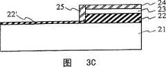
(a)如图3A所示,在由Si支持基片21、埋入氧化膜22、SOI层23构成的SOI单晶片20上,形成由硅氧化膜(SiO2)和硅氮化膜(SiN Si3N4等)或者它们的复合膜构成的掩模图案24。(a) As shown in FIG. 3A, on the SOI
(b)如图3B所示,以RIE(reactive ion etching)等的各向异性蚀刻除去未由掩模图案保护的区域的SOI层23和埋入绝缘膜22。这时,为了防止对Si支持基片21的机械损伤和等离子区损伤,在SOI单晶片20的埋入氧化膜22′稍有保留的状态下结束蚀刻。(b) As shown in FIG. 3B, the
(c)如图3C所示,为了保护露出的SOI层23的侧面,形成侧壁保护膜25。作为侧壁保护膜25,可以适用硅氮化膜(Si3N4)和硅氧化膜(SiO2)。将其全面堆积后,经RIE进行侧壁保留,形成侧壁保护膜25。在侧壁保留时,调整侧壁保护膜25和在支持基片21上保留的埋入氧化膜22′的膜厚,使先前保留的埋入氧化膜22′仍维持在支持基片21上。(c) As shown in FIG. 3C , in order to protect the exposed side surfaces of the
(d)如图3D所示,使用例如NH4F和HF等腐蚀剂对支持基片21上保留很少的埋入氧化膜22′进行湿式蚀刻,无损伤地露出支持基片21的表面。在所定前处理后,用通过化学汽相生长产生的选择外延生长,在露出的支持基片21上形成单晶体Si层26。(d) As shown in FIG. 3D , use an etchant such as NH4 F and HF to perform wet etching on the buried
前工序中,在使用硅氧化膜(SiO2)作为侧壁保护膜的情况下,当对用以保护硅基片21的保留的薄埋入氧化膜22′进行湿式蚀刻时,侧壁保护膜25也被少许蚀刻。然而,由于用以保护支持基片21表面的残留埋入氧化膜22′的膜厚足够薄,则可不露出SOI层侧壁,仅露出支持基片21的表面。In the preceding process, in the case where a silicon oxide film (SiO2 ) is used as the sidewall protection film, when the remaining thin buried oxide film 22' for protecting the
另一方面,在使用硅氮化膜(Si3N4)作为侧壁保护膜25时,加工控制性良好。第1实施例中,如后所述,在后工序去掉侧壁保护膜25,最后产品中并未保留块状元件区域11和SOI元件区域12边界的侧壁保护膜25。因此,即使使用Si3N4作为侧壁保护膜25时,也不会有应力产生的问题,使加工控制性优先。On the other hand, when a silicon nitride film (Si3 N4 ) is used as the sidewall
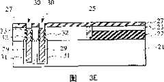
(e)如图3E所示,除去残留在SOI基片表面的掩模图案24,在整个面上形成新的掩模材料27。当事先掩模图案24是Si3N4时,可用磷酸除去。,当事先掩模图案24是SiO2时,可用HF(氢氟酸)除去。这时,侧壁保护膜25也因掩模图案24的蚀刻,至少一部分被蚀刻,但该部分由掩模材料27埋入。新形成的掩模材料27也是SiO2、Si3N4、或者它们的复合膜。使掩模材料27形成图案,将其作为掩模,形成DRAM的沟道电容器30。沟道电容器30也可用所希望的方法形成。例如,用RIE等形成沟道后,形成下部扩散片31,通过介质膜(未图示)埋入n型聚硅等存储电极29。形成有色绝缘膜32,再埋入沟道,在上部形成用于与一个单元晶体管的n型源极/漏极扩散层40a(参照图2)进行电连接的带状构件33,最后用n型聚硅等埋入。(e) As shown in FIG. 3E, the
(f)如图3F所示,在块状元件区域11和SOI元件区域12,一起形成元件分离35a、35b。具体地说,使掩模材料27形成图案,在块状元件区域11和SOI元件区域,以同样的深度形成元件分离用浅沟道。将掩模材料27作为限制器在沟道内埋入绝缘膜,同时形成块状元件区域11的第1元件分离35a和SOI元件区域12的第2元件分离35b。(f) As shown in FIG. 3F , in the
设定能以同等蚀刻速度蚀刻硅层和硅氧化膜的条件,为使DRAM单元的带状构件33与外围电路和SOI元件的所有元件分离,将SOI元件区域12的元件分离用沟道和块状元件区域11的元件分离用沟道以相同的速率掘进到必要的深度,填充同样的绝缘材料。因此,一起形成了块状元件区域11的第1元件分离35a和SOI元件区域12的第2元件分离35b。Set the conditions under which the silicon layer and the silicon oxide film can be etched at the same etching rate. In order to separate the strip-shaped
(g)最后,如图3G所示,将沟道内的埋入绝缘膜蚀刻达到SOI层23和外延成长层26的表面,除去掩模材料27。在除去掩模材料27时,或者通过新的蚀刻工序,除去了侧壁保护膜25的至少一部分,形成洼陷46,用硅系列材料埋入洼陷46,形成图2所示边界层47。洼陷46的埋入可在独立的工序中进行,也可在栅电极39、41制作的同时埋入。前者情况下,洼陷46埋入后,根据需要进行陷阱和沟道的掺杂质,在所定位置形成使栅极绝缘膜48介子中间的栅电极39、41(参照图2)和源极·漏极40、42。后者情况下,用聚硅和SiGe等硅系列材料形成栅电极,栅电极形成时,洼陷46自动地由栅极材料埋入。其结果是SOI层23和Si单晶体的外延成长层26的边界,同样由硅系列膜47连接。(g) Finally, as shown in FIG. 3G , the buried insulating film in the trench is etched to reach the surface of the
图2所示栅电极39、41形成后,按照所希望的MOSFET形成工序,经层间绝缘膜和布线工序,完成混装DRAM宏结构和SOI逻辑的半导体装置。元件形成时,在对栅电极和源极·漏极采用辅助加工的情况下,为防止在边界埋入的聚硅47变形,最好用掩模等保护聚硅47。After the
如图2一点划线所示,将边界层47作为图案突出时,洼陷46本身用聚硅保护,可进行辅助加工。As shown by the dot-dash line in FIG. 2, when the boundary layer 47 is protruded as a pattern, the
图2的例子中,SOI层23和埋入氧化膜22加在一起的厚度比较厚,支持基片21和外延成长层26的界面设置在比较深的位置。为了使DRAM存储单元43的带状构件部33的pn接合面和单元部的源极·漏极40a、40b可靠地从支持基片21和外延成长层26的界面分离,在低于界面的较浅位置形成该pn接合面。即使由于加工不适合使界面状态恶化,也可用于防止接合漏泄维持存储单元的保持特性。In the example of FIG. 2, the combined thickness of the
第1实施例的半导体装置中,用聚硅、SiGe等硅系列材料连接在块状元件区域11的外延成长层26和SOI层23之间,则可抑制区域间应力产生的结晶缺陷。In the semiconductor device of the first embodiment, silicon series materials such as polysilicon and SiGe are used to connect between the epitaxial growth layer 26 and the
并且,也可防止区域间应力产生的移动度变动,有效地防止边界附近的元件恶化。In addition, it is also possible to prevent fluctuations in mobility due to stress between regions, and effectively prevent deterioration of elements near the boundary.
由于在保护原来SOI层侧壁的侧壁保护膜的位置设置边界层,则可抑制芯片面积增大。Since the boundary layer is provided at the position of the sidewall protective film that protects the sidewall of the original SOI layer, an increase in the chip area can be suppressed.
由于块状元件区域和SOI元件区域的元件形成面是一样的高度,则有利于栅电极的平版印刷等后工序。Since the element formation surfaces of the bulk element region and the SOI element region are at the same height, it is beneficial to post-processes such as lithography of the gate electrode.
由于SOI元件区域的元件分离与具有沟道电容器的块状元件区域的元件分离是相同深度,尽管SOI元件区域侧的元件分离的表面积是微细的,也可有效地防止漏泄电流。并且,可以具有足够余量地形成元件分离的埋入条件。Since the device separation in the SOI device region is at the same depth as the device separation in the bulk device region having trench capacitors, leak current can be effectively prevented even though the surface area of the device separation on the SOI device region side is fine. Also, the embedding conditions for element isolation can be formed with a sufficient margin.
如图2所示,将SOI逻辑和DRAM装载在同一芯片上的系统单片型半导体装置,与将逻辑和DRAM置于不同芯片的情况相比,可以高速度、低耗电地进行数据交换。As shown in FIG. 2, a system-on-a-chip semiconductor device in which SOI logic and DRAM are mounted on the same chip can exchange data at high speed and low power consumption compared to the case where logic and DRAM are placed on different chips.
由于块状元件区域11不仅含有DRAM存储单元43,还有包含周围电路44和其他电路元件的一个功能块(DRAM宏结构),则可将原来在块状基片开发的DRAM电路设计和设备没计仍然用于SOI/块状基片。当然,不仅是DRAM宏结构,用块状基片开发的其他功能宏结构,例如模拟电路宏结构、高耐压电路宏结构、DRAM以外的存储电路宏结构等都可适用。Since the
第1实施例的制造方法中,按相同沟道深度一起形成元件形成面高度大致相等的块状元件区域和SOI元件区域的元件分离。因此,在埋入所必要绝缘膜的膜厚和埋入蚀刻时间等加工条件方面大体上不会产生差别,则简化了元件分离形成作业。In the manufacturing method of the first embodiment, the device separation of the bulk device region and the SOI device region having substantially the same height of the device forming surface is formed together at the same trench depth. Therefore, there is substantially no difference in processing conditions such as the film thickness of the insulating film required for embedding and the etching time for embedding, and the work of forming element isolation is simplified.
<第2实施例><Second embodiment>
图4是本发明第2实施例的半导体装置50的概略剖面图。半导体装置50具有:支持基片50;在支持基片51上形成的外延成长层56上形成元件43、44的块状元件区域11;在支持基片51的埋入氧化膜52上的SOI层53上形成元件45的SOI元件区域12;分离块状元件区域内的各元件43、44的第1元件分离65a;分离SOI元件区域12内的各元件45的第2元件分离65b;位于块状元件区域11和SOI元件区域12边界的第3元件分离65c。本例中,第3元件分离65c为边界层。FIG. 4 is a schematic cross-sectional view of a
第2实施例中,由在块状元件区域11形成的元件43、44、其他电路元件(未图示)构成DRAM宏结构,由在SOI元件区域12形成的元件45构成SOI逻辑。In the second embodiment,
第1~第3元件分离65a~65c都设定在相同深度,而且,深于SOI元件区域12的埋入氧化膜52。形成DRAM单元43等的块状元件区域11的元件形成面和形成MOSFET45的SOI元件区域12的元件形成面是大致一样的高度,构成DRAM宏结构的元件43、44和构成SOI逻辑的元件45位于大致相同高度。The first to
块状元件区域11具有作为块状成长层的单晶体Si的外延成长层56。SOI元件区域12由硅支持基片51、埋入氧化膜52、SOI膜53构成,埋入氧化膜52和SOI层53加在一起的厚度设定成稍小于第1实施例。由于埋入氧化膜52较薄,则可更有效地使SOI元件动作产生的热量向支持基片51发散,这在防止元件特性恶化方面是必要的。The
第2实施例的半导体装置50,在边界部具有与分别配置在块状元件区域11和SOI元件区域12的元件分离同样深度、材料的元件分离65c。位于边界的元件分离65c与其他元件分离65a、65b同样,深于埋入氧化膜53。因此,可以防止从边界部分的错位等缺陷扩展到块状元件区域的外延成长层56。The
图5A~5C是图4所示半导体装置50的制造工序图。图5A是继续图30的工序,图3A~30的工序,除埋入氧化膜的膜厚不同之外,与第1实施例是共同的,则其详细说明省略。5A to 5C are manufacturing process diagrams of the
第1实施例中,通过用硅系列材料连接去掉了侧壁保护膜的区域间的边界部分,解决了应力问题。然而,当与侧壁保护膜连接的外延层受到损伤时,则为不完全处置。In the first embodiment, the problem of stress is solved by connecting the boundary portions between the regions from which the sidewall protection film has been removed by using a silicon-based material. However, when the epitaxial layer connected to the sidewall protective film is damaged, it is incomplete disposal.
第2实施例的制造方法中,准备了埋入氧化膜厚度比较薄的SOI基片,使元件分离用沟道较深,设定元件分离的深度深于SOI元件区域的埋入氧化膜。并且,通过在块状元件区域11和SOI元件区域12的边界部配置元件分离用沟道,在各区域内的元件分离沟道形成的同时,一举去掉了残留在边界的侧壁保护膜和在边界附近结晶性恶化的部分。In the manufacturing method of the second embodiment, an SOI substrate having a relatively thin buried oxide film is prepared, the device isolation trench is made deep, and the buried oxide film is set to have a device isolation depth deeper than that of the SOI device region. Furthermore, by arranging element isolation trenches at the boundary between the
具体地说,如图5A所示,覆盖整个块状元件区域的外延成长层56、SOI基片的SOI层53、侧壁保护膜55,形成掩模材料57。将掩模材料57按所定形状形成图案后,与第1实施例一样,形成DRAM的沟道电容器30。Specifically, as shown in FIG. 5A , the
此后,如图5B所示,在块状元件区域、SOI元件区域、以及它们的边界一起形成元件分离用沟道。这时,通过对硅、聚硅、硅氧化膜设定具有同等蚀刻速度的蚀刻条件,可用相同的蚀刻时间一起形成相同深度的沟道。任一个沟道都深于SOI元件区域的埋入氧化膜52。由于残存的侧壁保护膜55的深度最大达埋入氧化膜52的深度,则在元件分离沟道形成的同时,在侧壁保护膜55和边界部分,一起除去了结晶性恶化的区域。此后,通过用同一绝缘材料埋入沟道内,一起形成块状元件区域(DRAM宏结构)的第1元件分离65a、SOI元件区域(SOI逻辑)的第2元件分离65b、以及位于边界的第3元件分离65c。Thereafter, as shown in FIG. 5B , element isolation trenches are formed in the bulk element region, the SOI element region, and their boundaries. At this time, by setting etching conditions having the same etching rate for silicon, polysilicon, and silicon oxide films, trenches of the same depth can be formed together with the same etching time. Either trench is deeper than the buried
最后,如图5C所示,对沟道内的埋入绝缘膜进行背面腐蚀,除去掩模材料57,在所定位置形成元件43、44、45,完成图4所示半导体装置50。Finally, as shown in FIG. 5C , the buried insulating film in the trench is etched back to remove the
第2实施例的半导体装置和其制造方法中,位于边界的元件分离65c深于埋入氧化膜53,则一起除去了侧壁保护膜和其邻近的结晶恶化部分。因此缓和了应力,并可防止由于应力的影响从边界部的错位等缺陷扩展到外延成长层56。In the semiconductor device and its manufacturing method of the second embodiment, the
并且,也是可将已有的元件分离构造适用于区域间边界的标准。In addition, it is also a standard that can apply the existing device separation structure to the boundary between regions.
芯片面积增大的有效抑制、元件形成面高度的均等化产生的效果,与第1实施例一样。The effects of effectively suppressing the increase in the chip area and equalizing the height of the element forming surface are the same as those of the first embodiment.
<第3实施例><Third embodiment>
图6是本发明第3实施例的半导体装置70的概略剖面图。半导体装置70具有:形成DRAM单元83和外围晶体管84的块状元件区域11;形成MOSFET85的SOI元件区域12;在块状元件区域11形成的第1元件分离79;在SOI区域12形成的第2元件分离75、75a,第2元件分离75、75a浅于第1元件分离79。FIG. 6 is a schematic cross-sectional view of a
块状元件区域11和SOI元件区域12的任一个元件分离中,位于最靠近边界的元件分离75a兼用作区域间的边界层。图7的例子中,位于SOI元件区域12的第2元件分离中,最靠边界侧的元件分离75a,兼用位于块状元件区域11和SOI元件区域12这间的边界,在元件分离层75a的底面,与SOI元件区域12的埋入氧化膜72连接。当然,通过设计,位于块状元件区域11最靠边界侧的元件分离79也可以兼用边界层。这时,图中未表示,作为边界的元件分离79重叠在SOI元件区域12的端部的元件分离75a和其下方的埋入氧化膜72。Among the device isolations of the
块状元件区域11具有作为块状成长层的外延成长层76,由DRAM单元83、外围晶体管84、以及其他电路元件(未图示)构成DRAM宏结构。SOI元件区域12由SOI层73、埋入氧化膜72以及硅支持基片71构成,由MOSFET85构成SOI逻辑。这些元件通过块状元件区域11和SOI元件区域12,位于同样的高度。The
这样,第3实施例的半导体装置70中,在块状元件区域11和SOI元件区域12,为了设定适合各个区域的元件分离,第1元件分离79的深度和第2元件分离75的深度不同。而且,任一个区域的元件分离中,位于最靠近边界的元件分离(图7例子中,SOI元件区域的元件分离75a),兼用块状元件区域11和SOI元件区域12的区域间边界层。Thus, in the
第3实施例的半导体装置70中,在块状元件区域11和SOI元件区域12分别设置最适合深度元件分离的理由如下。In the
第1实施例和第2实施例中,所有的元件分离为相同构成,然而在逻辑部特别要求元件分离的微细化。在要求高度微细化的情况下,为了形成比在SOI基片上埋入氧化膜更深的沟道,必须精密控制对SOI层侧壁蚀刻时的沟道锥形角以及对埋入氧化膜侧壁蚀刻时的沟道锥形角。若不精密地进行角度控制,则在埋入沟道后,内部留有空洞,空洞内残存栅电极材料,可能引起布线短路。In the first embodiment and the second embodiment, all the elements are separated into the same configuration, however, in the logic part, the miniaturization of the element separation is particularly required. When a high degree of miniaturization is required, in order to form a channel deeper than that of the buried oxide film on the SOI substrate, it is necessary to precisely control the taper angle of the channel when etching the sidewall of the SOI layer and the etching of the sidewall of the buried oxide film. channel taper angle at . If the angle is not precisely controlled, after the trench is buried, there will be a cavity inside, and the gate electrode material will remain in the cavity, which may cause a short circuit in the wiring.
因此,在逻辑部特别要求微细化的情况下,通过在SOI元件区域设置最适当的元件分离区域,增加了应力缓和、有效抑制元件面积增大、元件形成面高度一致化等效果,防止了布线短路,确保动作的可靠性。Therefore, in the case where miniaturization is particularly required in the logic part, by setting the most appropriate element isolation area in the SOI element area, the effects of stress relaxation, effective suppression of element area increase, and uniform element formation surface height are increased, preventing wiring. Short circuit to ensure the reliability of the action.
半导体装置70中,块状元件区域11和SOI元件区域12的任一个区域的元件分离,都有在边界部的边界层功能。因此,可以在最边界处形成元件,静区缩小了,能有效地抑制芯片面积的增大。In the
由于在块状元件区域11和SOI元件区域12分别配置最适当的元件分离,由可防止在SOI元件区域的元件分离内部发生空洞,抑制栅电极的短路等。By arranging the most appropriate device isolation in the
图7A~7F是第3实施例的半导体装置70的制造工序图。7A to 7F are manufacturing process diagrams of the
(a)首先,如图7A所示,在SOI元件区域12内的所定位置和块状元件区域的边界跨越双方区域的位置,形成浅的元件分离75、75a。具体地说,在整个SOI基片面上堆积硅氮化膜等掩模材料,使其图案化形成第1掩模74。在覆盖第1掩模74的以外地方,通过RIE等形成浅的沟道,堆积SiO2等的绝缘膜形成文件分离75、75a。这些元件分离75、75a为位于SOI元件区域的第2元件分离。(a) First, as shown in FIG. 7A ,
(b)如图7B所示,用保护膜等在整个面上形成第2掩模材料77,覆盖整个SOI元件区域和位于边界的元件分离75a,使第2掩模材料77形成图案。将该第2掩模材料77作为掩模,依次蚀刻除去第1掩模材料74、SOI层73、边界的元件分离75a的一部分、以及埋入氧化膜72。最好通过RIE除去第1掩模材料74、SOI层73、元件分离75a、以及到达埋入氧化膜72的中途,当最后露出硅支持基片71时,进行湿式蚀刻。(b) As shown in FIG. 7B, a second mask material 77 is formed on the entire surface with a protective film or the like to cover the entire SOI device region and the
通过RIE蚀刻时,即使SOI元件区域SOI层73的侧面不特地形成侧壁保护膜,而由位于边界的第2元件分离75a保护。由于埋入氧化膜72和位于边界的第2元件分离75a都是SiO2系列复合膜,所以在最后露出块状元件区域的硅支持基片71的阶段进行湿式蚀刻处理。通过该湿式蚀刻,可以不损伤支持基片71地除去埋入氧化膜72以及第2元件分离75a中突出于块状元件区域侧的部分。When etching by RIE, even if the side wall of the
(c)如图7C所示,除去第2掩模材料77,在露出的硅支持基片71上,使单晶体硅有选择地外延成长,形成外延成长层76。这样,在SOI基片内形成了块状元件区域。(c) As shown in FIG. 7C , the second mask material 77 is removed to selectively epitaxially grow monocrystalline silicon on the exposed
(d)如图7D所示,必要时除去第1掩模图案74后,全面形成新的掩模材料78,制成图案,在块状元件区域形成沟道电容器30。沟道电容器30的形成方法已在第1实施例中说明。(d) As shown in FIG. 7D , after removing the
(e)如图7E所示,在块状元件区域,形成比第2元件分离75更深的第1元件分离79。(e) As shown in FIG. 7E , the
(f)最后,如图7F所示,背面腐蚀沟道内的埋入绝缘膜,掩模材料78除去后,形成构成DRAM和SOI逻辑的晶体管83、84、85,完成半导体装置70。(f) Finally, as shown in FIG. 7F, the buried insulating film in the trench is etched on the back side, and the
图8A~8C是图6所示半导体装置70的另一个制造工序图。在图7所示制造工序中,当形成块状元件区域时,仅在SOI元件区域内和边界上形成浅的元件分离75、75a,在形成块状元件区域的预定SOI基片上,残存掩模材料74。在图8所示制造工序中,由于晶体成长在整个块状化的预定区域,预先形成元件分离层75a。8A to 8C are diagrams showing another manufacturing process of the
首先,如图8A所示,在全面堆积第1掩膜材料74后,仅使SOI元件区域12内的元件形成部分形成图案。其他部分,即在SOI元件区域12内的一部分(形成元件分离区域)和整个块状化的区域,例如形成SiO2的元件分离用绝缘膜75、75a。First, as shown in FIG. 8A , after depositing the
然后,如图8B所示,将残存在SOI元件区域和连接块状化区域的边界部分上的第2掩模材料77形成图案。接着,最好利用湿式蚀刻一次除去形成块状成长层的区域的元件分离用绝缘膜75a和埋入氧化膜72。这样,在自动保护SOI区域的SOI层73侧壁的状态下,即可用一次蚀刻露出硅支持基片71。由于连续地湿式蚀刻除去元件分离绝缘膜75和埋入氧化膜75a,则不会对硅支持基片71的表面造成损伤。Then, as shown in FIG. 8B , the second mask material 77 remaining on the boundary portion between the SOI device region and the connection bulk region is patterned. Next, the insulating
再如图8C所示,在露出的硅支持基片71上,利用选择外延成长形成外延成长层76。As shown in FIG. 8C , on the exposed
以后的工序与图7D~7F一样。图8所示制造方法中,在露出块状区域的硅支持基片时,利用一次湿式蚀刻就可完成。因此,在块状元件区域和SOI元件区域,即使形成不同深度、不同材料的元件分离,就整体来看,制造工序简化了。Subsequent steps are the same as those shown in FIGS. 7D to 7F. In the manufacturing method shown in FIG. 8, when the silicon support substrate in the bulk region is exposed, it can be completed by one wet etching. Therefore, even if device separations of different depths and different materials are formed in the bulk device region and the SOI device region, the manufacturing process is simplified as a whole.
图7和图8所示的任一种制造方法中,在SOI元件区域的元件分离形成后,由于进行伴随高温工序的外延成长和沟道电容器形成,则可期待通过加工的最佳化,缓和SOI元件区域的应力。In any of the manufacturing methods shown in Fig. 7 and Fig. 8, after the element isolation formation of the SOI element region, since the epitaxial growth and the formation of the trench capacitor accompanied by the high temperature process are performed, it can be expected that the process can be optimized to ease Stress in the SOI component region.
并且,可在块状元件区域和SOI元件区域都以一样的高度形成元件。Also, devices can be formed at the same height in both the bulk device region and the SOI device region.
由于预先在边界部形成属于块状元件区域和SOI元件区域任一个的元件分离75a,则可自动保护SOI层的侧面。因此,不再需要独立的侧壁保护膜形成工序。Since the
当露出块状元件区域部的支持基片时,由于可对埋入氧化膜和位于边界的元件分离用绝缘膜进行湿式蚀刻处理,则可避免对支持基片的损伤。When the supporting substrate in the bulk element region is exposed, since the buried oxide film and the insulating film for element isolation at the boundary can be wet-etched, damage to the supporting substrate can be avoided.
<第4实施例><Fourth embodiment>
图9A和9B表示本发明第4实施例的半导体装置。第4实施例对第2实施例和第3实施例进行了组合,在边界部配置了深于埋入氧化膜的独立的元件分离,在全部除去包含侧壁保护膜在内的边界部结晶缺陷的同时,在各区域设置最适合的元件分离。9A and 9B show a semiconductor device according to a fourth embodiment of the present invention. In the fourth embodiment, the second embodiment and the third embodiment are combined, an independent element isolation deeper than the buried oxide film is arranged at the boundary portion, and crystal defects at the boundary portion including the sidewall protection film are completely removed. At the same time, the most suitable component separation is set in each area.
图9A的例子,半导体装置90A具有:支持基片91;在支持基片91上形成的外延成长层96上形成元件98、94的块状元件区域11;在位于支持基片91的埋入氧化膜92上的SOI层93上形成元件45的SOI元件区域12。还具有:分离块状元件区域11内的各元件98、94的第1元件分离95a;分离SOI元件区域12内的各元件45的第2元件分离95b;位于块状元件区域11和SOI元件区域12的边界的第3元件分离95c。SOI元件区域内的第2元件分离95b比块状元件区域11内的第1元件分离95a和位于边界的第3元件分离95c更浅。边界部的第3元件分离95c比SOI元件区域12的埋入氧化膜92更深。In the example of FIG. 9A , the
形成DRAM单元98等的块状元件区域11的元件形成面和形成MOSFET45的SOI元件区域12的元件形成面,大致是一样高度,构成DRAM宏结构的元件98、94和构成SOI逻辑的元件45,位于大致一样的高度。The element formation surface of the
制作图9A所示半导体装置90A时,一直到DRAM的沟道电容器30的制造工序,与图3A~3E是一样的,此后,以同样的平版印刷工序形成块状元件区域11的第1元件分离95a和位于边界的第3元件分离95c,并同时除去侧壁保护膜,也可用另外的平版印刷工序形成SOI元件区域12内的第2元件分离95b。图9A的例子中,位于边界的第3元件分离95c多少进入了SOI层93,而且,由于蚀刻条件,有时也进入埋入氧化膜92。当接近边界形成SOI元件区域12端部的第2元件分离95b时,也可以使第3元件分离95c和边界附近的第2元件分离95b为一体。When manufacturing the
图9B所示半导体装置90B,设定分离块状元件区域11内的DRAM单元98的第1元件分离97a和SOI元件区域12内的第2元件分离97b为相同深度,而比位于边界的第3元件分离97c更浅。边界部的元件分离97c,为了除掉外延成长时的结晶缺陷,必须设定得比埋入氧化膜92深。另外,为了减少沟道电容器30的存储电极29的引出电阻,与分离SOI零件区域12的MOSFET45的第2元件分离97b同样浅地形成第1元件分离97a。这样,适合每个区域的元件分离是可能的。块状元件区域11内的外围电路44的元件分离97d,可以与边界部的第3元件分离97c同时以同样的深度、同样的材料形成,或者与DRAM单元的第1元件分离97a和SOIMOSFET45的第2元件分离97b同时形成。In the
图9A、9B的任一个例子中,在块状元件区域内形成的DRAM单元等元件和在SOI元件区域形成的MOSFET等元件的高度,大致为一定的。In either of the examples shown in FIGS. 9A and 9B , the heights of elements such as DRAM cells formed in the bulk element region and elements such as MOSFETs formed in the SOI element region are substantially constant.
由于与元件分离一起除去了在邻近边界的区域可能受到损伤的块状成长层76,则消除了应力问题。并且,由于可在块状元件区域和SOI元件区域分别形成最适合的元件分离,则动作的可靠性提高了。防止芯片面积增大和元件形成面高度均等化产生的效果,与第3实施例是一样的。Since the
<第5实施例><Fifth embodiment>
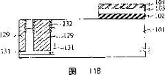
图10是本发明第5实施例的半导体装置100的概略剖面图。第5实施例提供了一种将在块状元件区域11形成的电路元件作为沟道电容器型DRAM单元的情况下,可以实现块状基片内的有效利用,增大存储容量,或者以同样存储容量进一步提高密度的系统单片型半导体装置。FIG. 10 is a schematic cross-sectional view of a semiconductor device 100 according to a fifth embodiment of the present invention. The fifth embodiment provides a case where the circuit element formed in the
半导体装置100具有:支持基片101;在支持基片101上形成的外延成长层106上形成DRAM单元143的块状元件区域11;在位于支持基片101上的埋入氧化膜102上的SOI层103上形成元件45的SOI元件区域12。还有:分离块状元件区域11内的DRAM单元143的第1元件分离105a;分离SOI元件区域12内的各元件45的第2元件分离105b;位于块状元件区域11和SOI元件区域12的边界的第3元件区域分离105c。第3元件分离105c,在图10的例子中,独立地位于边界,比SOI元件区域12的埋入氧化膜102更深。不言而喻,如参照图6已说明的第3实施例一样,SOI元件区域最靠边界侧的元件分离105b,或者块状元件区域最靠边界侧的元件分离105d,可以兼作边界层。The semiconductor device 100 has: a
位于块状元件区域11内的DRAM单元143具有沟道电容器130。沟道电容器130由位于与外延成长层106的界面下方的支持基片101内的第1部分以及位于界面上方的外延成长层106内的第2部分构成,第1部分宽方向的横剖面积比第2部分宽方向的横剖面积宽阔。换言之,沟道电容器130的第1部分在块状成长层106的界面以下区域,延伸到DRAM单元晶体管的栅极39a正下方的至少一部分。The
在单元晶体管正下方,由于沟道电容器130扩张,则可不增加DRAM单元阵列(未图示)整体面积,增加存储容量。Right below the cell transistors, due to the expansion of the
具有这种电容器构成的系统单片型半导体装置100,除去SOI基片所定位置的SOI层103和埋入氧化膜102,露出支持基片101,有效地利用从露出面使块状层结晶成长的工序。当用仅装载DRAM的单功能芯片实现图10的构成时,在块状基片上形成沟道电容器的宽幅第1部分后,必须用另外办法在基片表面实施使硅外延成长的工序。然而,在系统单片型半导体装置中,利用SOI/块状基片制作工序,将沟道电容器的剖面形状调整为所希望的形状,即可实现存储容量的增大。In the system monolithic semiconductor device 100 having such a capacitor structure, the
图11表示这种系统单片型半导体装置100的制造工序。FIG. 11 shows the manufacturing process of such a system monolithic semiconductor device 100 .
(a)首先,如图11A所示,在由Si支持基片101、埋入氧化膜102、SOI层103构成的SOI单晶片上,由任意掩模材料(例如SiO2和SiN,Si3N4等)或其复合膜形成掩模图案104。利用RIE等除去掩模图案104未保护区域的SOI层103和埋入绝缘膜102,部分地露出Si基片101。为了减少对Si支持基片101的损伤,可以对埋入氧化膜102除去的最后阶段进行湿式蚀刻。(a) First, as shown in FIG. 11A, on an SOI single wafer composed of a
(b)如图11B所示,在露出的Si支持基片101上形成DRAM的沟道电容器的第1部分。例如,利用RIE形成沟道后,再形成下部扩散片131、电介质膜(未图示),埋入聚硅等存储电极129。形成有色绝缘膜132,埋入残存的沟道,制作从露出的Si支持基片101表面向下方延伸的第1部分。(b) As shown in FIG. 11B, the first portion of the trench capacitor of the DRAM is formed on the exposed
(c)如图11C所示,在沟道电容器第1部分的上部形成限制器133和保护SOI基片的露出侧壁的侧壁保护膜134。限制器133和侧壁保护膜134例如都是硅氮化膜。(c) As shown in FIG. 11C, a
(d)如图11D所示,形成与SOI元件区域的SOI层103相同高度的外延成长层106。外延成长层106例如通过以二氯硅烷作为源气体的选择外延成长形成。(d) As shown in FIG. 11D , an
(e)如图11E所示,全面地形成掩模图案114,形成到达在前面工序中形成的沟道电容器130的第1部分的开口部。该开口部的剖面形状小于位于Si支持基片102内的第1部分的剖面形状。在开口的侧壁形成侧壁氧化膜135,填充聚硅,形成沟道电容器130的第2部分。在该第2部分,对Si支持基片102内的第1部分和在上部形成的晶体管进行电连接。(e) As shown in FIG. 11E , a
(f)如图11F所示,形成块状元件区域11内的第1元件分离105a、SOI元件区域12内的第2元件分离105b、位于这些区域的边界的第3元件分离105c。当形成第3元件分离105c时,全部除去位于边界的侧壁保护膜134。图中未图示的构成DRAM宏结构的外围电路元件的元件分离也在这个阶段形成。第3元件分离105c和第1及第2元件分离105a、105b,也可以在另一个工序中制作。或者,在对硅氧化膜的蚀刻速率与对硅氮化膜的蚀刻速率进行比较是非常小的蚀刻条件下,也可同时形成。由于沟道电容器130的第2部分(在外延成长层106形成的部分)的剖面比较小,为了抑制电阻的增大,最好第1元件分离105a与SOI元件区域12的第2元件分离105b是同样高度。(f) As shown in FIG. 11F, the
(g)最后,如图11G所示,形成DRAM单元的晶体管143、构成SOI逻辑电路的MOSFET45。并且,形成未图示的DRAM宏结构的外围电路144,完成图10所示半导体装置100。(g) Finally, as shown in FIG. 11G, the
图12表示图10所示半导体装置的变形例。图12的半导体装置是组合了图10所示第5实施例的DRAM单元和图6所示第3实施例的边界元件分离构造。并同时表示在块状元件区域11和SOI元件区域12的元件形成面上层形成的多层布线的构成例。FIG. 12 shows a modified example of the semiconductor device shown in FIG. 10 . The semiconductor device shown in FIG. 12 is a combination of the DRAM cell of the fifth embodiment shown in FIG. 10 and the boundary element separation structure of the third embodiment shown in FIG. 6 . Also shown are configuration examples of multilayer wiring formed on the device forming surfaces of the
图12的半导体装置具有:分离块状元件区域11内的DRAM单元143的第1元件分离107a;分离SOI元件区域12内的各元件45的第2元件分离107b和107c,最靠近边界的元件分离107c兼用作边界层。The semiconductor device of FIG. 12 has: a
在DRAM单元143的上层有位线125和字线126,还具有将DRAM单元143的漏极连接到位线125的位线接点124。在SOI元件区域12,在MOSFET45的源极·漏极上,配置用于降低电阻的硅化物123,插头128连接上层的Al布线127和MOSFET45。On the upper layer of the
制作这种半导体装置时,采用图7A和7B的方法或者图8A和8B的方法,预先形成SOI元件区域12的第2元件分离区域107b、107c,在所定位置露出的Si支持基片101。然后,如图11B所示,在露出的Si基片上形成沟道电容器130的宽幅的第1部分。此后,形成覆盖第1部分的限制器133后,在Si支持基片上通过选择外延成长形成块状成长层106。当外延成长时,在边界部分预先形成的第2元件分离区域107c具有侧壁保护膜的作用。在外延成长层106上形成构成沟道电容器130的窗部的第2部分,并形成块状元件区域11的第1元件分离107a。而且,在每个区域形成DRAM单元143(参照图10)、SOIMOSFET45、外围电路144等。再形成保护膜122和SOIMOSFET的源极·漏极上的硅化物123,堆积层间绝缘膜121。形成将DRAM单元晶体管143的漏极连接到位线125的位线接点124、将SOIMOSFET连接到上层布线127的插头128,用通常的方法形成上层岂有此理线124、126、127。When manufacturing such a semiconductor device, the second
图12的半导体装置中,由于有效利用DRAM单元晶体管正下方的Si支持基片101区域,将沟道电容器延设在单元晶体管的下方,则可增大存储容量或电容器配置密度。同时,由于SOI元件区域12的元件分离107c兼用边界层和侧壁保护膜,则可减少边界部的应力,防止芯片面积增大。并且,通过选择外延成长,使得块状成长层106和SOI层103的元件形成面的高度一定,则可在同一水平上配置不同功能的电路元件。In the semiconductor device shown in FIG. 12 , since the
<第6实施例><Sixth embodiment>
图13是本发明第6实施例的半导体装置200的概略剖面图。FIG. 13 is a schematic cross-sectional view of a
半导体装置200具有:在Si支持基片201的块状成长层(外延成长层)206上形成DRAM单元213、外围晶体管214等元件的块状元件区域11;在埋入氧化膜202的SOI层203上形成MOSFET5等元件的SOI元件区域12;位于这些区域的边界的边界层207;在块状元件区域内,位于与SOI元件区域的边界附近的重置图案(空置电容器)240。The
形成DRAM单元213等的块状成长层206与形成MOSFET216的SOI层203的高度大致相等。The height of the
半导体装置200还具有:在块状元件区域11内分离各元件的第1元件分离205a;在SOI元件区域12内分离各元件的第2元件分离205b。图13的例子中,第1元件分离205a和第2元件分离205b的深度一样,但也可以将SOI元件区域12的SOI元件分离205b作为达到埋入氧化膜202表面的浅的元件分离。后者情况下,由于相对于硅的蚀刻速率设定了氧化膜的蚀刻速率极小的蚀刻条件,则可在同一工序中一起形成。The
空置电容器240的深度,设定深于SOI元件区域12的埋入氧化膜202。若在块状元件区域11和SOI元件区域12的边界部发生错位,如箭头A所示,即使向块状元件区域11扩展,由于空置电容器240的存在,也可以防止错位向块状元件区域11内部的扩张。The depth of the
图13的例子中,空置图案被设置为与在块状元件区域11内形成的DRAM单元213的沟道电容器230相同形状、相同构成的空置电容器240。因而,具有用与沟道电容器的埋入电极229同样材料埋入并作为下部电极的扩散层231和有色侧壁217。然而,未设置上部带状构件等,则可以仅是埋入与沟道电容器230相同形状沟道的空置图案。在空置电容器240的表面部分,形成如第1元件分离205a一样的元件分离,使其具有电的不活性。In the example of FIG. 13 , the dummy pattern is provided as a
图13的例子中,在具有图2所示硅系列边界层207的半导体装置中设置空置电容器240,但也可以在具有图4所示边界独立的元件分离65c的半导体装置中设置空置电容器240。如图7所示,在SOI元件区域12内的元件分离75a兼用边界层的半导体装置中,也可以在块状元件区域11内的边界附近设置空置电容器240。在具有图10所示剖面形状的沟道电容器的半导体装置中,在边界附近的块状元件区域11内,可以配置相同形状或其他形状的空置电容器。任何一种情况下,空置电容器都深于SOI元件区域12的埋入氧化膜。In the example of FIG. 13, the
空置图案在外延成长层206形成后,开始形成。如图13所示半导体装置200,在块状元件区域11内具有包含沟道电容器的DRAM单元的情况下,最好在沟道电容器230形成的同时,在同样工序中一起形成。The dummy pattern starts to form after the
图14是表示图13所示空置电容器240配置的平面图。图14的例子表示在块状元件区域内的边界部,配置与DRAM单元的沟道电容器230相同的构造的空置电容器240的情况。空置电容器240可以不一定是与沟道电容器230相同构造,然而,采用相同构造,可以使加工条件与存储单元形成完全一致地形成空置电容器。空置电容器的深度被设定在深于SOI元件区域的埋入氧化膜。FIG. 14 is a plan view showing the arrangement of
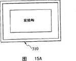
图15表示空置图案的变形例。图15A表示用线状空置图案310包围块状元件区域11内的宏结构(例如DRAM宏结构)的变形例,图15B表示用岛状空量图案311包围宏结构(例如DRAM宏结构)的变形例。任一个例子都是在形成外延成长等的块状成长层后形成。在形成DRAM宏结构的情况下,与DRAM的沟道电容器形成的同时,可形成空置图案310、311。这时,使线状空置图案情况下的线宽、岛状空置图案情况下的短边长度,都与DRAM单元的电容器图案的短边长度配合,仍然用存储单元的加工处理,即可同时形成空置图案。FIG. 15 shows a modified example of the dummy pattern. FIG. 15A shows a modification example of enclosing a macrostructure (such as a DRAM macrostructure) in a block-shaped
第6实施例中,除了在边界部的应力缓和、元件形成面的均匀平坦化、芯片面积抑制增大等方面的效果外,由于在块状元件区域内的边界附近配置空置图案,则可以防止边界部分的错位扩展到块状元件区域内。In the sixth embodiment, in addition to the effects of relaxation of stress at the boundary, uniform flattening of the element formation surface, and suppression of increase in chip area, since dummy patterns are arranged near the boundary in the bulk element region, it is possible to prevent The misalignment of the border portion extends into the block element area.
<其他实施例><Other Embodiments>
第1实施例到第5实施例中,在除去SOI基片的一部分形成块状元件区域时,利用单晶体硅的选择外延成长形成块状成长层。然而,作为块状元件区域,也可以使SiGe外延成长。并且,利用非选择外延成长也能形成块状成长层。In the first to fifth embodiments, when a part of the SOI substrate is removed to form a bulk element region, a bulk growth layer is formed by selective epitaxial growth of single crystal silicon. However, it is also possible to epitaxially grow SiGe as a bulk element region. In addition, a bulk growth layer can also be formed by non-selective epitaxial growth.
在一个SOI基片内,可使Si的块状成长层和SiGe(硅锗)的块状成长层共存。这时,用与在各区域形成的元件的栅电极材料相同的聚硅和SiGe等填充各块状元件区域和SOI基片的边界,由在块状元件区域和SOI基片的边界,则在块状元件区域和SOI元件区域的边界或者不同块状元件区域之间的边界,可使应力最小,提高容限。In one SOI substrate, a bulk growth layer of Si and a bulk growth layer of SiGe (silicon germanium) can coexist. At this time, fill the boundary between each block element region and the SOI substrate with the same polysilicon and SiGe as the gate electrode material of the element formed in each region, and then in the boundary between the block element region and the SOI substrate Boundaries between bulk component regions and SOI component regions or between different bulk component regions can minimize stress and improve tolerance.
若在SOI元件区域和Si块状元件区域、或者SOI元件区域和SiGe块状元件区域的边界,配置在各区域内使用的元件分离,则减少了静区。If the devices used in each region are arranged separately at the boundary between the SOI device region and the Si bulk device region, or between the SOI device region and the SiGe bulk device region, the dead zone is reduced.
具体的构成例是:在Si块状元件区域形成DRAM,在SiGe的块状元件区域形成双极电路,即可形成将双方与SOI基片上的逻辑电路一起装载在1个芯片上的半导体装置。根据在各块状元件区域和SOI元件区域形成的元件和功能块的性质,可以形成各个最适合的元件分离,从第3~第5实施例可见,可能是在性能方面最出色的系统LSI。A specific configuration example is to form a DRAM in the bulk device region of Si and form a bipolar circuit in the bulk device region of SiGe to form a semiconductor device in which both are mounted on a single chip together with the logic circuit on the SOI substrate. According to the properties of the devices and functional blocks formed in the respective bulk device regions and SOI device regions, each optimal device separation can be formed, and it can be seen from the third to fifth embodiments that the system LSI may be the most excellent in terms of performance.
在Si块状元件区域或SiGe元件区域内,在与SOI元件区域的边界附近,由于形成了比埋入绝缘膜更深的空置图案,则可防止在边界部经常发生的错位扩展到块状元件区域内。该空置图案在使用沟道电容器时,可以是与电容器构造同样的构成,在使用纵型双极性晶体管时,为了分离集电极,可以是与一般使用的更深的元件分离同样的构成。此外,SOI基片的埋入绝缘膜并不限定埋入氧化膜。In the Si bulk element region or SiGe element region, near the boundary with the SOI element region, since the dummy pattern is formed deeper than the buried insulating film, it is possible to prevent dislocations that often occur at the boundary from spreading to the bulk element region Inside. The dummy pattern may have the same configuration as a capacitor structure when using a trench capacitor, or may have the same configuration as a generally used deeper device isolation for separating collectors when using a vertical bipolar transistor. In addition, the buried insulating film of the SOI substrate is not limited to the buried oxide film.
上述各实施例中,通过调节元件分离沟道的蚀刻条件,可以有各种变形构造。In each of the above-mentioned embodiments, by adjusting the etching conditions of the element isolation trenches, various modified structures are possible.
例如,图4所示第2实施例中,可在硅和氧化膜相同程度的蚀刻速率的加工条件下,一起形成元件分离65a、65b、65c,也可以在氧化膜的蚀刻速度较慢的条件下一起形成。这时,SOI元件区域内的元件分离65b比块状元件区域内的元件分离65a更浅。并且,位于边界部的元件分离65c的形状为非对称。也就是,在埋入氧化膜52上形成与SOI元件区域侧的元件分离65b同等深度,在块状成长层56侧形成与元件分离65a相同深度。为了完全除去边界部的侧壁保护膜的影响和受到结晶恶化的块状成长层,希望元件分离65a的深度比支持基片51和埋入氧化膜52的界面更深。For example, in the second embodiment shown in FIG. 4, the
块状元件区域内和边界部的元件分离65a、65c与SOI元件区域内的元件分离65b,可以在各自的蚀刻工序中以不同的蚀刻条件形成。例如,在一个蚀刻工序中,在对硅和氧化膜相同的蚀刻速率的条件下加工元件分离65a和65c,在对氧化膜的蚀刻速率较慢的条件下加工元件分离65b。这时,位于边界部的元件分离65c的形状是对称的,不用担心产生应力,并且由于形成较浅的SOI元件区域内的元件分离65b,则可实现容易埋入的微细的元件分离。The
如上所述,由于将SOI元件区域和块状元件区域的元件形成面设定为同样高度,则可排除对后面制造工序的不良影响。As described above, since the device formation surfaces of the SOI device region and the bulk device region are set at the same height, adverse effects on subsequent manufacturing processes can be eliminated.
由于在SOI元件区域和块状元件区域的边界配置了适当的边界层,则可以减少区域之间的应力。Since an appropriate boundary layer is arranged at the boundary between the SOI element area and the bulk element area, the stress between the areas can be reduced.
由于合理地实现了位于边界部的元件分离的配置构成,则可抑制芯片面积的增大。Since the configuration in which the elements at the boundary portion are separated is rationally realized, an increase in the chip area can be suppressed.
Claims (28)
Applications Claiming Priority (2)
| Application Number | Priority Date | Filing Date | Title |
|---|---|---|---|
| JP2001298533 | 2001-09-27 | ||
| JP2001298533AJP4322453B2 (en) | 2001-09-27 | 2001-09-27 | Semiconductor device and manufacturing method thereof |
Publications (2)
| Publication Number | Publication Date |
|---|---|
| CN1411066A CN1411066A (en) | 2003-04-16 |
| CN100342539Ctrue CN100342539C (en) | 2007-10-10 |
Family
ID=19119420
Family Applications (1)
| Application Number | Title | Priority Date | Filing Date |
|---|---|---|---|
| CNB021495181AExpired - Fee RelatedCN100342539C (en) | 2001-09-27 | 2002-09-27 | Semiconductor device and mfg. method thereof |
Country Status (5)
| Country | Link |
|---|---|
| US (3) | US6835981B2 (en) |
| JP (1) | JP4322453B2 (en) |
| KR (1) | KR100547059B1 (en) |
| CN (1) | CN100342539C (en) |
| TW (1) | TWI261911B (en) |
Families Citing this family (160)
| Publication number | Priority date | Publication date | Assignee | Title |
|---|---|---|---|---|
| US6956757B2 (en) | 2000-06-22 | 2005-10-18 | Contour Semiconductor, Inc. | Low cost high density rectifier matrix memory |
| TWI230392B (en) | 2001-06-18 | 2005-04-01 | Innovative Silicon Sa | Semiconductor device |
| JP4322453B2 (en)* | 2001-09-27 | 2009-09-02 | 株式会社東芝 | Semiconductor device and manufacturing method thereof |
| KR100442781B1 (en)* | 2001-12-24 | 2004-08-04 | 동부전자 주식회사 | semiconductor having having trench capacitor and method for fabricating the same |
| JP3943932B2 (en)* | 2001-12-27 | 2007-07-11 | 株式会社東芝 | Manufacturing method of semiconductor device |
| US20050090053A1 (en)* | 2002-01-21 | 2005-04-28 | Infineon Technologies Ag | Memory chip with low-temperature layers in the trench capacitor |
| US6885080B2 (en)* | 2002-02-22 | 2005-04-26 | International Business Machines Corporation | Deep trench isolation of embedded DRAM for improved latch-up immunity |
| EP1357603A3 (en) | 2002-04-18 | 2004-01-14 | Innovative Silicon SA | Semiconductor device |
| EP1355316B1 (en) | 2002-04-18 | 2007-02-21 | Innovative Silicon SA | Data storage device and refreshing method for use with such device |
| JP3660650B2 (en)* | 2002-06-13 | 2005-06-15 | 株式会社東芝 | Manufacturing method of semiconductor device |
| KR100480892B1 (en)* | 2002-07-11 | 2005-04-07 | 매그나칩 반도체 유한회사 | Gate forming method of dual gate logic element |
| JP2004103611A (en) | 2002-09-04 | 2004-04-02 | Toshiba Corp | Semiconductor device and manufacturing method thereof |
| KR100481868B1 (en)* | 2002-11-26 | 2005-04-11 | 삼성전자주식회사 | Modified silicon-on-insulator substrate having isolation structure of preventing leakage current and method of fabricating the same |
| US20040222485A1 (en)* | 2002-12-17 | 2004-11-11 | Haynie Sheldon D. | Bladed silicon-on-insulator semiconductor devices and method of making |
| JP3944087B2 (en)* | 2003-01-21 | 2007-07-11 | 株式会社東芝 | Method for manufacturing element forming substrate |
| JP2004228273A (en)* | 2003-01-22 | 2004-08-12 | Renesas Technology Corp | Semiconductor device |
| US6902962B2 (en)* | 2003-04-04 | 2005-06-07 | Taiwan Semiconductor Manufacturing Company, Ltd. | Silicon-on-insulator chip with multiple crystal orientations |
| US6912150B2 (en) | 2003-05-13 | 2005-06-28 | Lionel Portman | Reference current generator, and method of programming, adjusting and/or operating same |
| US7085153B2 (en) | 2003-05-13 | 2006-08-01 | Innovative Silicon S.A. | Semiconductor memory cell, array, architecture and device, and method of operating same |
| US20040228168A1 (en)* | 2003-05-13 | 2004-11-18 | Richard Ferrant | Semiconductor memory device and method of operating same |
| US7202118B1 (en)* | 2003-06-13 | 2007-04-10 | Advanced Micro Devices, Inc. | Fully depleted SOI MOSFET arrangement with sunken source/drain regions |
| US7329923B2 (en)* | 2003-06-17 | 2008-02-12 | International Business Machines Corporation | High-performance CMOS devices on hybrid crystal oriented substrates |
| US7335934B2 (en) | 2003-07-22 | 2008-02-26 | Innovative Silicon S.A. | Integrated circuit device, and method of fabricating same |
| JP4167565B2 (en)* | 2003-07-31 | 2008-10-15 | 株式会社東芝 | Method for manufacturing partial SOI substrate |
| US20050045992A1 (en)* | 2003-08-27 | 2005-03-03 | Turley Alfred P. | Bipolar/thin film SOI CMOS structure and method of making same |
| JP2005072084A (en)* | 2003-08-28 | 2005-03-17 | Toshiba Corp | Semiconductor device and manufacturing method thereof |
| US7184298B2 (en) | 2003-09-24 | 2007-02-27 | Innovative Silicon S.A. | Low power programming technique for a floating body memory transistor, memory cell, and memory array |
| JP2005197405A (en)* | 2004-01-06 | 2005-07-21 | Toshiba Corp | Semiconductor device and manufacturing method thereof |
| JP4322706B2 (en)* | 2004-02-27 | 2009-09-02 | 株式会社東芝 | Manufacturing method of semiconductor device |
| US6995456B2 (en)* | 2004-03-12 | 2006-02-07 | International Business Machines Corporation | High-performance CMOS SOI devices on hybrid crystal-oriented substrates |
| US6949420B1 (en)* | 2004-03-12 | 2005-09-27 | Sony Corporation | Silicon-on-insulator (SOI) substrate having dual surface crystallographic orientations and method of forming same |
| JP4177775B2 (en) | 2004-03-16 | 2008-11-05 | 株式会社東芝 | Semiconductor substrate, manufacturing method thereof, and semiconductor device |
| US7087965B2 (en) | 2004-04-22 | 2006-08-08 | International Business Machines Corporation | Strained silicon CMOS on hybrid crystal orientations |
| KR100968305B1 (en)* | 2004-06-16 | 2010-07-08 | 인터내셔널 비지네스 머신즈 코포레이션 | STI formation in a semiconductor device comprising a SOI and a bulk silicon region |
| US7118986B2 (en) | 2004-06-16 | 2006-10-10 | International Business Machines Corporation | STI formation in semiconductor device including SOI and bulk silicon regions |
| US7094634B2 (en)* | 2004-06-30 | 2006-08-22 | International Business Machines Corporation | Structure and method for manufacturing planar SOI substrate with multiple orientations |
| US7186622B2 (en)* | 2004-07-15 | 2007-03-06 | Infineon Technologies Ag | Formation of active area using semiconductor growth process without STI integration |
| KR100555569B1 (en) | 2004-08-06 | 2006-03-03 | 삼성전자주식회사 | A semiconductor device having a channel region limited by an insulating film and its manufacturing method |
| EP1630863B1 (en)* | 2004-08-31 | 2014-05-14 | Infineon Technologies AG | Method of fabricating a monolithically integrated vertical semiconducting device in an soi substrate |
| US7274073B2 (en)* | 2004-10-08 | 2007-09-25 | International Business Machines Corporation | Integrated circuit with bulk and SOI devices connected with an epitaxial region |
| JP3998677B2 (en)* | 2004-10-19 | 2007-10-31 | 株式会社東芝 | Manufacturing method of semiconductor wafer |
| US7338848B1 (en)* | 2004-10-20 | 2008-03-04 | Newport Fab, Llc | Method for opto-electronic integration on a SOI substrate and related structure |
| US7235433B2 (en)* | 2004-11-01 | 2007-06-26 | Advanced Micro Devices, Inc. | Silicon-on-insulator semiconductor device with silicon layers having different crystal orientations and method of forming the silicon-on-insulator semiconductor device |
| US7476939B2 (en) | 2004-11-04 | 2009-01-13 | Innovative Silicon Isi Sa | Memory cell having an electrically floating body transistor and programming technique therefor |
| JP4552603B2 (en)* | 2004-11-08 | 2010-09-29 | エルピーダメモリ株式会社 | Manufacturing method of semiconductor device |
| US7251164B2 (en) | 2004-11-10 | 2007-07-31 | Innovative Silicon S.A. | Circuitry for and method of improving statistical distribution of integrated circuits |
| US7229877B2 (en)* | 2004-11-17 | 2007-06-12 | International Business Machines Corporation | Trench capacitor with hybrid surface orientation substrate |
| US7301838B2 (en) | 2004-12-13 | 2007-11-27 | Innovative Silicon S.A. | Sense amplifier circuitry and architecture to write data into and/or read from memory cells |
| US7301803B2 (en) | 2004-12-22 | 2007-11-27 | Innovative Silicon S.A. | Bipolar reading technique for a memory cell having an electrically floating body transistor |
| US20060175659A1 (en)* | 2005-02-07 | 2006-08-10 | International Business Machines Corporation | A cmos structure for body ties in ultra-thin soi (utsoi) substrates |
| GB0508407D0 (en)* | 2005-04-26 | 2005-06-01 | Ami Semiconductor Belgium Bvba | Alignment of trench for MOS |
| JP2006324415A (en)* | 2005-05-18 | 2006-11-30 | Toshiba Corp | Semiconductor wafer, semiconductor device, and method of manufacturing semiconductor device |
| US20070023833A1 (en)* | 2005-07-28 | 2007-02-01 | Serguei Okhonin | Method for reading a memory cell having an electrically floating body transistor, and memory cell and array implementing same |
| KR100650870B1 (en)* | 2005-08-08 | 2008-07-16 | 주식회사 하이닉스반도체 | Flash memory device and manufacturing method thereof |
| JP2009507389A (en)* | 2005-09-06 | 2009-02-19 | エヌエックスピー ビー ヴィ | Manufacturing method of semiconductor device having isolation region and device manufactured by the method |
| US7606066B2 (en) | 2005-09-07 | 2009-10-20 | Innovative Silicon Isi Sa | Memory cell and memory cell array having an electrically floating body transistor, and methods of operating same |
| US7355916B2 (en) | 2005-09-19 | 2008-04-08 | Innovative Silicon S.A. | Method and circuitry to generate a reference current for reading a memory cell, and device implementing same |
| US20070085140A1 (en)* | 2005-10-19 | 2007-04-19 | Cedric Bassin | One transistor memory cell having strained electrically floating body region, and method of operating same |
| US20070105302A1 (en)* | 2005-11-09 | 2007-05-10 | Infineon Technologies Ag | Integrated circuit formed on a semiconductor substrate |
| JP4972917B2 (en)* | 2005-11-25 | 2012-07-11 | 株式会社デンソー | Semiconductor device and manufacturing method thereof |
| US7683430B2 (en) | 2005-12-19 | 2010-03-23 | Innovative Silicon Isi Sa | Electrically floating body memory cell and array, and method of operating or controlling same |
| US8530355B2 (en) | 2005-12-23 | 2013-09-10 | Infineon Technologies Ag | Mixed orientation semiconductor device and method |
| US7542345B2 (en) | 2006-02-16 | 2009-06-02 | Innovative Silicon Isi Sa | Multi-bit memory cell having electrically floating body transistor, and method of programming and reading same |
| JP5145691B2 (en)* | 2006-02-23 | 2013-02-20 | セイコーエプソン株式会社 | Semiconductor device |
| US7795661B2 (en)* | 2006-03-07 | 2010-09-14 | International Business Machines Corporation | Vertical SOI transistor memory cell |
| US7666721B2 (en)* | 2006-03-15 | 2010-02-23 | International Business Machines Corporation | SOI substrates and SOI devices, and methods for forming the same |
| DE102006013721B4 (en)* | 2006-03-24 | 2011-12-08 | Infineon Technologies Ag | Semiconductor circuit arrangement and associated method for temperature detection |
| DE102006015076B4 (en)* | 2006-03-31 | 2014-03-20 | Advanced Micro Devices, Inc. | Semiconductor device with SOI transistors and solid-state transistors and a method for manufacturing |
| US7285480B1 (en)* | 2006-04-07 | 2007-10-23 | International Business Machines Corporation | Integrated circuit chip with FETs having mixed body thicknesses and method of manufacture thereof |
| US7492632B2 (en) | 2006-04-07 | 2009-02-17 | Innovative Silicon Isi Sa | Memory array having a programmable word length, and method of operating same |
| US7606098B2 (en) | 2006-04-18 | 2009-10-20 | Innovative Silicon Isi Sa | Semiconductor memory array architecture with grouped memory cells, and method of controlling same |
| US7933142B2 (en) | 2006-05-02 | 2011-04-26 | Micron Technology, Inc. | Semiconductor memory cell and array using punch-through to program and read same |
| JP2007329200A (en)* | 2006-06-06 | 2007-12-20 | Toshiba Corp | Manufacturing method of semiconductor device |
| US7569450B2 (en)* | 2006-06-09 | 2009-08-04 | International Business Machines Corporation | Semiconductor capacitors in hot (hybrid orientation technology) substrates |
| US8069377B2 (en) | 2006-06-26 | 2011-11-29 | Micron Technology, Inc. | Integrated circuit having memory array including ECC and column redundancy and method of operating the same |
| US7542340B2 (en) | 2006-07-11 | 2009-06-02 | Innovative Silicon Isi Sa | Integrated circuit including memory array having a segmented bit line architecture and method of controlling and/or operating same |
| US7494918B2 (en)* | 2006-10-05 | 2009-02-24 | International Business Machines Corporation | Semiconductor structures including multiple crystallographic orientations and methods for fabrication thereof |
| US7592209B2 (en)* | 2006-11-13 | 2009-09-22 | Intel Corporation | Integration of a floating body memory on SOI with logic transistors on bulk substrate |
| DE102007034402B4 (en)* | 2006-12-14 | 2014-06-18 | Advanpack Solutions Pte. Ltd. | Semiconductor package and manufacturing method therefor |
| US8368144B2 (en)* | 2006-12-18 | 2013-02-05 | Infineon Technologies Ag | Isolated multigate FET circuit blocks with different ground potentials |
| KR101277402B1 (en) | 2007-01-26 | 2013-06-20 | 마이크론 테크놀로지, 인코포레이티드 | Floating-body dram transistor comprising source/drain regions separated from the gated body region |
| US7772048B2 (en)* | 2007-02-23 | 2010-08-10 | Freescale Semiconductor, Inc. | Forming semiconductor fins using a sacrificial fin |
| US7759773B2 (en)* | 2007-02-26 | 2010-07-20 | International Business Machines Corporation | Semiconductor wafer structure with balanced reflectance and absorption characteristics for rapid thermal anneal uniformity |
| US20090096066A1 (en)* | 2007-10-10 | 2009-04-16 | Anderson Brent A | Structure and Method for Device-Specific Fill for Improved Anneal Uniformity |
| US7679166B2 (en)* | 2007-02-26 | 2010-03-16 | International Business Machines Corporation | Localized temperature control during rapid thermal anneal |
| US7692275B2 (en)* | 2007-02-26 | 2010-04-06 | International Business Machines Corporation | Structure and method for device-specific fill for improved anneal uniformity |
| US7745909B2 (en)* | 2007-02-26 | 2010-06-29 | International Business Machines Corporation | Localized temperature control during rapid thermal anneal |
| US8518774B2 (en) | 2007-03-29 | 2013-08-27 | Micron Technology, Inc. | Manufacturing process for zero-capacitor random access memory circuits |
| US7485965B2 (en)* | 2007-05-25 | 2009-02-03 | International Business Machines Corporation | Through via in ultra high resistivity wafer and related methods |
| US8064274B2 (en) | 2007-05-30 | 2011-11-22 | Micron Technology, Inc. | Integrated circuit having voltage generation circuitry for memory cell array, and method of operating and/or controlling same |
| US8085594B2 (en) | 2007-06-01 | 2011-12-27 | Micron Technology, Inc. | Reading technique for memory cell with electrically floating body transistor |
| WO2009039169A1 (en) | 2007-09-17 | 2009-03-26 | Innovative Silicon S.A. | Refreshing data of memory cells with electrically floating body transistors |
| US7933133B2 (en)* | 2007-11-05 | 2011-04-26 | Contour Semiconductor, Inc. | Low cost, high-density rectifier matrix memory |
| US8278731B2 (en) | 2007-11-20 | 2012-10-02 | Denso Corporation | Semiconductor device having SOI substrate and method for manufacturing the same |
| US8536628B2 (en) | 2007-11-29 | 2013-09-17 | Micron Technology, Inc. | Integrated circuit having memory cell array including barriers, and method of manufacturing same |
| US8349662B2 (en) | 2007-12-11 | 2013-01-08 | Micron Technology, Inc. | Integrated circuit having memory cell array, and method of manufacturing same |
| US7713814B2 (en)* | 2008-01-04 | 2010-05-11 | International Business Machines Corporation | Hybrid orientation substrate compatible deep trench capacitor embedded DRAM |
| US8773933B2 (en) | 2012-03-16 | 2014-07-08 | Micron Technology, Inc. | Techniques for accessing memory cells |
| US8014195B2 (en) | 2008-02-06 | 2011-09-06 | Micron Technology, Inc. | Single transistor memory cell |
| US8189376B2 (en) | 2008-02-08 | 2012-05-29 | Micron Technology, Inc. | Integrated circuit having memory cells including gate material having high work function, and method of manufacturing same |
| US7957206B2 (en) | 2008-04-04 | 2011-06-07 | Micron Technology, Inc. | Read circuitry for an integrated circuit having memory cells and/or a memory cell array, and method of operating same |
| FR2933233B1 (en)* | 2008-06-30 | 2010-11-26 | Soitec Silicon On Insulator | GOOD RESISTANCE HIGH RESISTIVITY SUBSTRATE AND METHOD FOR MANUFACTURING THE SAME |
| FR2933235B1 (en) | 2008-06-30 | 2010-11-26 | Soitec Silicon On Insulator | GOOD-WAY SUBSTRATE AND METHOD FOR MANUFACTURING THE SAME |
| FR2933236B1 (en)* | 2008-06-30 | 2010-11-26 | Soitec Silicon On Insulator | SUBSTRATE COMPRISING DIFFERENT TYPES OF SURFACE, AND METHOD OF MANUFACTURING THE SAME |
| FR2933234B1 (en)* | 2008-06-30 | 2016-09-23 | S O I Tec Silicon On Insulator Tech | GOODLY DUAL STRUCTURE SUBSTRATE AND METHOD FOR MANUFACTURING THE SAME |
| US7947543B2 (en) | 2008-09-25 | 2011-05-24 | Micron Technology, Inc. | Recessed gate silicon-on-insulator floating body device with self-aligned lateral isolation |
| US7933140B2 (en) | 2008-10-02 | 2011-04-26 | Micron Technology, Inc. | Techniques for reducing a voltage swing |
| US7924630B2 (en) | 2008-10-15 | 2011-04-12 | Micron Technology, Inc. | Techniques for simultaneously driving a plurality of source lines |
| US8223574B2 (en) | 2008-11-05 | 2012-07-17 | Micron Technology, Inc. | Techniques for block refreshing a semiconductor memory device |
| US8213226B2 (en) | 2008-12-05 | 2012-07-03 | Micron Technology, Inc. | Vertical transistor memory cell and array |
| US8319294B2 (en) | 2009-02-18 | 2012-11-27 | Micron Technology, Inc. | Techniques for providing a source line plane |
| WO2010102106A2 (en) | 2009-03-04 | 2010-09-10 | Innovative Silicon Isi Sa | Techniques for forming a contact to a buried diffusion layer in a semiconductor memory device |
| US8748959B2 (en) | 2009-03-31 | 2014-06-10 | Micron Technology, Inc. | Semiconductor memory device |
| US8139418B2 (en) | 2009-04-27 | 2012-03-20 | Micron Technology, Inc. | Techniques for controlling a direct injection semiconductor memory device |
| US8508994B2 (en) | 2009-04-30 | 2013-08-13 | Micron Technology, Inc. | Semiconductor device with floating gate and electrically floating body |
| US8188528B2 (en)* | 2009-05-07 | 2012-05-29 | International Buiness Machines Corporation | Structure and method to form EDRAM on SOI substrate |
| US8498157B2 (en) | 2009-05-22 | 2013-07-30 | Micron Technology, Inc. | Techniques for providing a direct injection semiconductor memory device |
| US8537610B2 (en) | 2009-07-10 | 2013-09-17 | Micron Technology, Inc. | Techniques for providing a semiconductor memory device |
| US8089126B2 (en)* | 2009-07-22 | 2012-01-03 | International Business Machines Corporation | Method and structures for improving substrate loss and linearity in SOI substrates |
| US9076543B2 (en) | 2009-07-27 | 2015-07-07 | Micron Technology, Inc. | Techniques for providing a direct injection semiconductor memory device |
| US8168507B2 (en)* | 2009-08-21 | 2012-05-01 | International Business Machines Corporation | Structure and method of forming enhanced array device isolation for implanted plate EDRAM |
| US8199595B2 (en) | 2009-09-04 | 2012-06-12 | Micron Technology, Inc. | Techniques for sensing a semiconductor memory device |
| US8395216B2 (en)* | 2009-10-16 | 2013-03-12 | Texas Instruments Incorporated | Method for using hybrid orientation technology (HOT) in conjunction with selective epitaxy to form semiconductor devices with regions of different electron and hole mobilities and related apparatus |
| US8174881B2 (en) | 2009-11-24 | 2012-05-08 | Micron Technology, Inc. | Techniques for reducing disturbance in a semiconductor device |
| US8310893B2 (en) | 2009-12-16 | 2012-11-13 | Micron Technology, Inc. | Techniques for reducing impact of array disturbs in a semiconductor memory device |
| US8416636B2 (en) | 2010-02-12 | 2013-04-09 | Micron Technology, Inc. | Techniques for controlling a semiconductor memory device |
| US8411513B2 (en) | 2010-03-04 | 2013-04-02 | Micron Technology, Inc. | Techniques for providing a semiconductor memory device having hierarchical bit lines |
| US8576631B2 (en) | 2010-03-04 | 2013-11-05 | Micron Technology, Inc. | Techniques for sensing a semiconductor memory device |
| US8369177B2 (en) | 2010-03-05 | 2013-02-05 | Micron Technology, Inc. | Techniques for reading from and/or writing to a semiconductor memory device |
| US8547738B2 (en) | 2010-03-15 | 2013-10-01 | Micron Technology, Inc. | Techniques for providing a semiconductor memory device |
| US8411524B2 (en) | 2010-05-06 | 2013-04-02 | Micron Technology, Inc. | Techniques for refreshing a semiconductor memory device |
| JP5592750B2 (en)* | 2010-10-14 | 2014-09-17 | 株式会社東芝 | Semiconductor device |
| CN102569648B (en)* | 2010-12-27 | 2014-09-03 | 中芯国际集成电路制造(北京)有限公司 | Phase change memory and manufacturing method thereof |
| CN102148251B (en)* | 2011-01-10 | 2013-01-30 | 电子科技大学 | SOI lateral MOSFET devices and integrated circuits |
| EP2477216A1 (en)* | 2011-01-13 | 2012-07-18 | Soitec | Hybrid bulk/SOI device with a buried doped layer and manufacturing method thereof |
| WO2012132219A1 (en)* | 2011-03-29 | 2012-10-04 | ルネサスエレクトロニクス株式会社 | Semiconductor device and manufacturing method for same |
| US9093538B2 (en)* | 2011-04-08 | 2015-07-28 | Semiconductor Energy Laboratory Co., Ltd. | Semiconductor device and method for manufacturing the same |
| US8531878B2 (en) | 2011-05-17 | 2013-09-10 | Micron Technology, Inc. | Techniques for providing a semiconductor memory device |
| US9559216B2 (en) | 2011-06-06 | 2017-01-31 | Micron Technology, Inc. | Semiconductor memory device and method for biasing same |
| CN102315154A (en)* | 2011-09-30 | 2012-01-11 | 上海宏力半导体制造有限公司 | Silicon-on-insulator structure and manufacturing method thereof as well as semiconductor device |
| DE102011087681A1 (en)* | 2011-12-02 | 2013-06-27 | Ihp Gmbh - Innovations For High Performance Microelectronics / Leibniz-Institut Für Innovative Mikroelektronik | Hetero-substrate for the production of integrated circuits with optical, opto-electronic and electronic components |
| JP2013168487A (en)* | 2012-02-15 | 2013-08-29 | Renesas Electronics Corp | Semiconductor device manufacturing method and semiconductor device |
| US8916426B2 (en) | 2012-03-27 | 2014-12-23 | International Business Machines Corporation | Passive devices for FinFET integrated circuit technologies |
| US8772902B2 (en)* | 2012-04-19 | 2014-07-08 | International Business Machines Corporation | Fabrication of a localized thick box with planar oxide/SOI interface on bulk silicon substrate for silicon photonics integration |
| US9093564B2 (en) | 2013-03-20 | 2015-07-28 | International Business Machines Corporation | Integrated passive devices for FinFET technologies |
| US9059041B2 (en) | 2013-07-02 | 2015-06-16 | International Business Machines Corporation | Dual channel hybrid semiconductor-on-insulator semiconductor devices |
| US9419134B2 (en) | 2014-01-13 | 2016-08-16 | Taiwan Semiconductor Manufacturing Company, Ltd. | Strain enhancement for FinFETs |
| US9543153B2 (en)* | 2014-07-16 | 2017-01-10 | Taiwan Semiconductor Manufacturing Co., Ltd. | Recess technique to embed flash memory in SOI technology |
| US9496280B1 (en)* | 2015-04-30 | 2016-11-15 | Globalfoundries Inc. | Semiconductor structure having logic region and analog region |
| US9728640B2 (en) | 2015-08-11 | 2017-08-08 | International Business Machines Corporation | Hybrid substrate engineering in CMOS finFET integration for mobility improvement |
| WO2017052645A1 (en)* | 2015-09-25 | 2017-03-30 | Intel Corporation | Method, device and system to provide capacitance for a dynamic random access memory cell |
| JP2018107253A (en)* | 2016-12-26 | 2018-07-05 | ルネサスエレクトロニクス株式会社 | Semiconductor device and manufacturing method of semiconductor device |
| KR102434436B1 (en) | 2017-05-31 | 2022-08-19 | 삼성전자주식회사 | Integrated circuit device and method of manufacturing the same |
| US11183452B1 (en) | 2020-08-12 | 2021-11-23 | Infineon Technologies Austria Ag | Transfering informations across a high voltage gap using capacitive coupling with DTI integrated in silicon technology |
| US11495660B2 (en)* | 2020-11-06 | 2022-11-08 | Globalfoundries Dresden Module One Limited Liability Company & Co. Kg | Co-integrated high voltage (HV) and medium voltage (MV) field effect transistors with defect prevention structures |
| KR20220091655A (en)* | 2020-12-23 | 2022-07-01 | 삼성전자주식회사 | Semiconductor device and method for manufacturing the same |
| CN115547919A (en)* | 2021-06-29 | 2022-12-30 | 上海华力集成电路制造有限公司 | Epitaxial growth method of FDSOI (fully-doped silicon on insulator) mixed region |
| US12020980B2 (en)* | 2021-07-07 | 2024-06-25 | Taiwan Semiconductor Manufacturing Company, Ltd. | Semiconductor structure and forming method thereof |
| DE112022005897T5 (en)* | 2021-12-10 | 2024-09-19 | X-Fab France SAS | SEMICONDUCTOR STRUCTURES AND METHODS |
| CN114899144A (en)* | 2022-04-14 | 2022-08-12 | 上海华力集成电路制造有限公司 | Method of forming a hybrid substrate |
Citations (10)
| Publication number | Priority date | Publication date | Assignee | Title |
|---|---|---|---|---|
| JPH06232367A (en)* | 1992-12-30 | 1994-08-19 | Samsung Electron Co Ltd | Dram based on silicon on insulator and manufacture thereof |
| JPH07106434A (en)* | 1993-10-05 | 1995-04-21 | Mitsubishi Electric Corp | Semiconductor memory device and manufacturing method thereof |
| JPH08316431A (en)* | 1995-05-22 | 1996-11-29 | Hitachi Ltd | Semiconductor device and manufacturing method thereof |
| CN1180931A (en)* | 1996-10-25 | 1998-05-06 | Lg半导体株式会社 | Method for forming field region of semiconductor device |
| JPH10303385A (en)* | 1997-04-25 | 1998-11-13 | Texas Instr Inc <Ti> | Hybrid device fabricated on SIMOX or bonded SOI substrate and method of manufacturing the same |
| JPH11238860A (en)* | 1998-02-19 | 1999-08-31 | Hitachi Ltd | Semiconductor integrated circuit device and method of manufacturing the same |
| JP2000091534A (en)* | 1998-09-11 | 2000-03-31 | Mitsubishi Electric Corp | Semiconductor device |
| WO2000048245A1 (en)* | 1999-02-12 | 2000-08-17 | Ibis Technology Corporation | Patterned silicon-on-insulator devices |
| CN1264157A (en)* | 1999-02-16 | 2000-08-23 | 国际商业机器公司 | Insulator base silicon structure of plane dense picture composition and manufacture technology thereof |
| CN1292572A (en)* | 1999-10-06 | 2001-04-25 | 三菱电机株式会社 | Semiconductor device and manufacturing method thereof |
Family Cites Families (25)
| Publication number | Priority date | Publication date | Assignee | Title |
|---|---|---|---|---|
| FR2547954B1 (en)* | 1983-06-21 | 1985-10-25 | Efcis | PROCESS FOR THE MANUFACTURE OF INSULATED SEMICONDUCTOR COMPONENTS IN A SEMICONDUCTOR WAFER |
| JPS6276645A (en)* | 1985-09-30 | 1987-04-08 | Toshiba Corp | Composite semiconductor crystal structure |
| JP2812388B2 (en)* | 1988-01-18 | 1998-10-22 | 富士通株式会社 | Method of manufacturing SOI semiconductor device |
| US5399507A (en)* | 1994-06-27 | 1995-03-21 | Motorola, Inc. | Fabrication of mixed thin-film and bulk semiconductor substrate for integrated circuit applications |
| EP0702411B1 (en)* | 1994-09-16 | 2002-11-27 | Kabushiki Kaisha Toshiba | High breakdown voltage semiconductor device with a buried MOS-gate structure |
| US6232649B1 (en)* | 1994-12-12 | 2001-05-15 | Hyundai Electronics America | Bipolar silicon-on-insulator structure and process |
| JP2806286B2 (en)* | 1995-02-07 | 1998-09-30 | 日本電気株式会社 | Semiconductor device |
| US5777362A (en)* | 1995-06-07 | 1998-07-07 | Harris Corporation | High efficiency quasi-vertical DMOS in CMOS or BICMOS process |
| US5705409A (en)* | 1995-09-28 | 1998-01-06 | Motorola Inc. | Method for forming trench transistor structure |
| JP3198959B2 (en)* | 1996-12-25 | 2001-08-13 | 富士電機株式会社 | High voltage integrated circuit |
| US5894152A (en)* | 1997-06-18 | 1999-04-13 | International Business Machines Corporation | SOI/bulk hybrid substrate and method of forming the same |
| US6214694B1 (en)* | 1998-11-17 | 2001-04-10 | International Business Machines Corporation | Process of making densely patterned silicon-on-insulator (SOI) region on a wafer |
| JP2000269460A (en) | 1999-03-18 | 2000-09-29 | Toshiba Corp | Semiconductor memory device and method of manufacturing the same |
| US6214653B1 (en)* | 1999-06-04 | 2001-04-10 | International Business Machines Corporation | Method for fabricating complementary metal oxide semiconductor (CMOS) devices on a mixed bulk and silicon-on-insulator (SOI) substrate |
| KR20010003206A (en)* | 1999-06-22 | 2001-01-15 | 김영환 | Method of manufacturing SOI device |
| US6333532B1 (en)* | 1999-07-16 | 2001-12-25 | International Business Machines Corporation | Patterned SOI regions in semiconductor chips |
| US6037199A (en)* | 1999-08-16 | 2000-03-14 | Taiwan Semiconductor Manufacturing Company, Ltd. | SOI device for DRAM cells beyond gigabit generation and method for making the same |
| US6287901B1 (en)* | 2000-01-05 | 2001-09-11 | International Business Machines Corporation | Method and semiconductor structure for implementing dual plane body contacts for silicon-on-insulator (SOI) transistors |
| JP2001196556A (en) | 2000-01-07 | 2001-07-19 | Toshiba Corp | Semiconductor device and method of manufacturing the same |
| US6465846B1 (en)* | 2000-03-22 | 2002-10-15 | Seiko Instruments Inc. | Semiconductor integrated circuit device having trench-type photodiode |
| US6350653B1 (en)* | 2000-10-12 | 2002-02-26 | International Business Machines Corporation | Embedded DRAM on silicon-on-insulator substrate |
| US6555891B1 (en)* | 2000-10-17 | 2003-04-29 | International Business Machines Corporation | SOI hybrid structure with selective epitaxial growth of silicon |
| US6635550B2 (en)* | 2000-12-20 | 2003-10-21 | Texas Instruments Incorporated | Semiconductor on insulator device architecture and method of construction |
| US6413857B1 (en)* | 2001-04-02 | 2002-07-02 | Advanced Micro Devices, Inc. | Method of creating ground to avoid charging in SOI products |
| JP4322453B2 (en)* | 2001-09-27 | 2009-09-02 | 株式会社東芝 | Semiconductor device and manufacturing method thereof |
- 2001
- 2001-09-27JPJP2001298533Apatent/JP4322453B2/ennot_activeExpired - Fee Related
- 2001-11-29USUS09/995,594patent/US6835981B2/ennot_activeExpired - Fee Related
- 2002
- 2002-09-17TWTW091121213Apatent/TWI261911B/ennot_activeIP Right Cessation
- 2002-09-26KRKR1020020058411Apatent/KR100547059B1/ennot_activeExpired - Fee Related
- 2002-09-27CNCNB021495181Apatent/CN100342539C/ennot_activeExpired - Fee Related
- 2004
- 2004-04-21USUS10/828,337patent/US7148543B2/ennot_activeExpired - Fee Related
- 2004-08-19USUS10/921,273patent/US7018904B2/ennot_activeExpired - Fee Related
Patent Citations (10)
| Publication number | Priority date | Publication date | Assignee | Title |
|---|---|---|---|---|
| JPH06232367A (en)* | 1992-12-30 | 1994-08-19 | Samsung Electron Co Ltd | Dram based on silicon on insulator and manufacture thereof |
| JPH07106434A (en)* | 1993-10-05 | 1995-04-21 | Mitsubishi Electric Corp | Semiconductor memory device and manufacturing method thereof |
| JPH08316431A (en)* | 1995-05-22 | 1996-11-29 | Hitachi Ltd | Semiconductor device and manufacturing method thereof |
| CN1180931A (en)* | 1996-10-25 | 1998-05-06 | Lg半导体株式会社 | Method for forming field region of semiconductor device |
| JPH10303385A (en)* | 1997-04-25 | 1998-11-13 | Texas Instr Inc <Ti> | Hybrid device fabricated on SIMOX or bonded SOI substrate and method of manufacturing the same |
| JPH11238860A (en)* | 1998-02-19 | 1999-08-31 | Hitachi Ltd | Semiconductor integrated circuit device and method of manufacturing the same |
| JP2000091534A (en)* | 1998-09-11 | 2000-03-31 | Mitsubishi Electric Corp | Semiconductor device |
| WO2000048245A1 (en)* | 1999-02-12 | 2000-08-17 | Ibis Technology Corporation | Patterned silicon-on-insulator devices |
| CN1264157A (en)* | 1999-02-16 | 2000-08-23 | 国际商业机器公司 | Insulator base silicon structure of plane dense picture composition and manufacture technology thereof |
| CN1292572A (en)* | 1999-10-06 | 2001-04-25 | 三菱电机株式会社 | Semiconductor device and manufacturing method thereof |
Also Published As
| Publication number | Publication date |
|---|---|
| TWI261911B (en) | 2006-09-11 |
| US20040195626A1 (en) | 2004-10-07 |
| US6835981B2 (en) | 2004-12-28 |
| KR100547059B1 (en) | 2006-01-31 |
| US7148543B2 (en) | 2006-12-12 |
| KR20030027749A (en) | 2003-04-07 |
| US7018904B2 (en) | 2006-03-28 |
| JP2003100900A (en) | 2003-04-04 |
| CN1411066A (en) | 2003-04-16 |
| JP4322453B2 (en) | 2009-09-02 |
| US20050019999A1 (en) | 2005-01-27 |
| US20030057487A1 (en) | 2003-03-27 |
Similar Documents
| Publication | Publication Date | Title |
|---|---|---|
| CN100342539C (en) | Semiconductor device and mfg. method thereof | |
| CN1229853C (en) | Manufacturing method of substrate for semiconductor device and substrate for semiconductor device | |
| CN1270380C (en) | Semiconductor device and its manufacturing method | |
| CN1237616C (en) | Semiconductor device with floating grid and mfg. method thereof | |
| CN1236494C (en) | Semiconductor device | |
| CN1205664C (en) | Semiconductor device and manufacturing method thereof | |
| CN1181552C (en) | Semiconductor device and manufacturing method thereof | |
| CN100336228C (en) | Semiconductor device | |
| CN1230905C (en) | Semiconductor device | |
| CN1249816C (en) | Semiconductor device and its mfg. method | |
| CN1855495A (en) | Field effect transistors with vertically oriented gate electrodes and methods for fabricating the same | |
| CN1286179C (en) | Nonvolatile semiconductor storing device and its manufacturing mehod | |
| CN1240131C (en) | Semiconductor device and manufacture thereof | |
| CN1309423A (en) | Semiconductor device and mfg method thereof | |
| CN1384547A (en) | Semiconductor device and its manufacture | |
| CN1836313A (en) | Strained-silicon-on-insulator single-and double-gate MOSFET and method for forming the same | |
| CN1925161A (en) | Semiconductor product and method for making a semiconductor product | |
| CN1223458A (en) | Semiconductor substrate processing method and semiconductor substrate | |
| CN1115716C (en) | Processing method of semiconductor substrate and semiconductor substrate | |
| CN1906755A (en) | Semiconductor manufacturing method and semiconductor device | |
| CN1514485A (en) | Non-volatile memory and manufacturing method thereof | |
| CN101043032A (en) | Semiconductor device and a method of manufacturing the same | |
| CN1411076A (en) | Semiconductor device and mfg. method thereof | |
| CN1421914A (en) | Semiconductor apparatus and producing method thereof | |
| CN1828831A (en) | Method for forming semiconductor substrate and formed semiconductor substrate |
Legal Events
| Date | Code | Title | Description |
|---|---|---|---|
| C06 | Publication | ||
| PB01 | Publication | ||
| C10 | Entry into substantive examination | ||
| SE01 | Entry into force of request for substantive examination | ||
| C14 | Grant of patent or utility model | ||
| GR01 | Patent grant | ||
| C17 | Cessation of patent right | ||
| CF01 | Termination of patent right due to non-payment of annual fee | Granted publication date:20071010 Termination date:20091027 |