CN100336300C - Reconfigurable Finite Impulse Response Filter - Google Patents
Reconfigurable Finite Impulse Response FilterDownload PDFInfo
- Publication number
- CN100336300C CN100336300CCNB031277306ACN03127730ACN100336300CCN 100336300 CCN100336300 CCN 100336300CCN B031277306 ACNB031277306 ACN B031277306ACN 03127730 ACN03127730 ACN 03127730ACN 100336300 CCN100336300 CCN 100336300C
- Authority
- CN
- China
- Prior art keywords
- digital
- coefficient
- digital processing
- multiplier
- processing unit
- Prior art date
- Legal status (The legal status is an assumption and is not a legal conclusion. Google has not performed a legal analysis and makes no representation as to the accuracy of the status listed.)
- Expired - Fee Related
Links
Images


Classifications
- H—ELECTRICITY
- H03—ELECTRONIC CIRCUITRY
- H03H—IMPEDANCE NETWORKS, e.g. RESONANT CIRCUITS; RESONATORS
- H03H17/00—Networks using digital techniques
- H03H17/02—Frequency selective networks
- H03H17/0294—Variable filters; Programmable filters
Landscapes
- Physics & Mathematics (AREA)
- Engineering & Computer Science (AREA)
- Computer Hardware Design (AREA)
- Mathematical Physics (AREA)
- Complex Calculations (AREA)
Abstract
Description
Translated fromChinese技术领域technical field
本发明涉及一种数字讯号处理机制,特别是涉及一种具有可重新配置(reconfigurable)能力的数字有限脉冲响应(Finite Impulse Response,FIR)滤波器。The present invention relates to a digital signal processing mechanism, in particular to a digital finite impulse response (Finite Impulse Response, FIR) filter with reconfigurable capability.
背景技术Background technique
有限脉冲响应(Finite Impulse Response,FIR)滤波器是数字通讯系统的一重要组件,业界一直致力于改善其滤波效能、减少硬件装置以及增进操作速度。除此之外,因为通讯系统对于集成化以及可重新配置能力的需求,软件无线电通讯系统开始获得注意,例如J.Mitola在“The Software RadioArchitecture,”IEEE Communications Magazine,vol.33,pp.26-38,May1995,或是E.Buracchini在“The Software Radio Concept,”IEEECommunications Magazine,vol.38,pp.138-143,Sept.2000,当中所提。为此,可重新配置的功能已成为未来滤波器设计的重要因素。The finite impulse response (Finite Impulse Response, FIR) filter is an important component of a digital communication system. The industry has been working on improving its filtering performance, reducing hardware devices, and increasing operating speed. In addition, because of the communication system's requirements for integration and reconfigurability, software radio communication systems have begun to gain attention, such as J.Mitola in "The Software Radio Architecture," IEEE Communications Magazine, vol.33, pp.26- 38, May1995, or E. Buracchini mentioned in "The Software Radio Concept," IEEE Communications Magazine, vol.38, pp.138-143, Sept.2000. For this reason, reconfigurable functionality has become an important factor in future filter designs.
有限脉冲响应滤波器可用来执行多种工作,例如匹配滤波、噪声隔绝、信道等化。也因此多种结构及实行方法被提出来,以加速和简化滤波器。然而,对于近来激增的有线及无线通讯标准,传统硬件结构已不适合未来通讯需求。另一方面,因为对可用于多种通讯标准的可重新配置通讯系统有强烈的需求,全世界有大量的研究人员投入软件无线电通讯系统的研发。依此种趋势看来,滤波器的结构设计必须考虑其系数重设和可重新配置的功能。Finite impulse response filters can be used to perform a variety of tasks such as matched filtering, noise isolation, and channel equalization. Therefore, various structures and implementation methods have been proposed to speed up and simplify the filter. However, for the recent proliferation of wired and wireless communication standards, traditional hardware structures are no longer suitable for future communication needs. On the other hand, since there is a strong demand for a reconfigurable communication system that can be used in various communication standards, a large number of researchers around the world are investing in the research and development of software defined radio communication systems. According to this trend, the structural design of the filter must consider its coefficient reset and reconfigurable functions.
一个典型的N个系数有限脉冲响应滤波器如下所述:A typical N coefficient finite impulse response filter is described as follows:
其中,in,
y[n]为一过滤后的数字讯号,n为该讯号的元素的一指数(index ofelements);y[n] is a filtered digital signal, and n is an index of elements of the signal;
hi为一滤波系数;且hi is a filter coefficient; and
x为一过滤前的数字讯号。x is a digital signal before filtering.
众所周知,标准化有号位(canonical signed digit,CSD)表示法可被用来减少一数字有限脉冲响应滤波器的复杂度,例如R.M.Hewlitt和E.S.Swartzlantler Jr.在“Canonical Signed Digit Representation for FIRDigital Filters”,Proc.of IEEE Workshop on Signal Processing Systems,2000,pp.416-426,中;M.Tamada和A.Nishihara在“High-Speed FIRDigital Filter with CSD Coefficients Implemented on FPGA”,Proc.ofthe ASP-DAC,2001,pp.7-8,中;以及Y.M.Hasan、L.J.Karem、M.Falkinburg、A.Helwig和M.Ronning在“Canonic Signed Digit ChebyshevFIR Filter Design”,IEEE Signal Processing Letters,vol.8,pp.167-169,June 2001,中所述。将滤波器系数使用CSD表示法编码可减少部分乘积的数目,进而在硬件制作上节省硅晶圆使用面积及减低功率消耗。因此此技术已被广泛应用于具有固定系数的有限脉冲响应滤波器。根据CSD表示法:It is well known that canonical signed digit (CSD) representations can be used to reduce the complexity of a digital finite impulse response filter, e.g. R.M. Hewlitt and E.S. Swartzlantler Jr. in "Canonical Signed Digit Representation for FIR Digital Filters", Proc.of IEEE Workshop on Signal Processing Systems, 2000, pp.416-426, in; M.Tamada and A.Nishihara in "High-Speed FIR Digital Filter with CSD Coefficients Implemented on FPGA", Proc.ofthe ASP-DAC, 2001 , pp.7-8, in; and Y.M. Hasan, L.J. Karem, M. Falkinburg, A. Helwig, and M. Ronning in "Canonic Signed Digit Chebyshev FIR Filter Design", IEEE Signal Processing Letters, vol.8, pp.167- 169, June 2001, described in. Encoding the filter coefficients using CSD notation can reduce the number of partial products, thereby saving silicon wafer area and reducing power consumption in hardware fabrication. Therefore this technique has been widely used in finite impulse response filters with fixed coefficients. According to CSD notation:
因此,therefore,
其中,in,
di,k为数值{1,0,-1}中的一元素;di, k is an element in the value {1, 0, -1};
pk为数值{0,…,L}中的一元素,L+1为系数的长度;而pk is an element in the value {0,...,L}, L+1 is the length of the coefficient; and
Mi为hi中非零数字的数目。Mi is the number of non-zero digits in hi .
当CSD表示法用于实现可重设系数的有限脉冲响应滤波器(programmable FIR filter)时,每一滤波器系数的功能可藉由相同数目的可重设定CSD来实现。然而,对大部分滤波器而言,只有少数系数需要极高的精确度。若是所有系数皆制作成高精确度的话,将会浪费宝贵的硬件资源。为了简化硬件,可重设系数有限脉冲响应滤波器通常限制每个系数可允许的非零CSD数目,如T.Zhangwen、Z.Zhanpeng、Z.Jie和M.Hao在“AHigh-Speed,Programmable,CSD Coefficient FIR Filter,”in Proc.of4th International Conference on ASIC,2001,pp.397-400,以及K.T.Hong、S.D.Yi和K.M.Chung在“A High-Speed Programmable FIR DigitalFilter Using Switching Arrays,”in Proc.of IEEE Asia PacificConference on Circuits and Systems,1996,pp.492-495,中所述。但是,此项限制可能减低系数的准确性和影响滤波器的频率响应,也可能因大部分系数使用多于所需的CSD而导致成本增加。一使用CSD系数的可重新配置有限脉冲响应滤波器曾被提出,如K.Y.Khoo、A.Kwentus和A.N.WillsonJr.在“A Programmable FIR Digital Filter Using CSD Coefficients,”IEEE Journal of Solid-State Circuits,vol.31,pp.869-874,June1996,中所述。此实行方法包含一个32-系数的线性相位滤波器,其每一系数具有二个非零CSD。额外的非零CSD可被分配至特定的滤波器的系数,以使有限脉冲响应滤波器可重新配置。然而,在此方法中某些运算资源仍然未被运用到,也使得关键延迟路径(critical delay path)在某些情况下相当地长。When the CSD notation is used to implement a programmable FIR filter with reconfigurable coefficients, the function of each filter coefficient can be realized by the same number of reconfigurable CSDs. However, for most filters, only a few coefficients require extreme precision. If all coefficients are made with high precision, precious hardware resources will be wasted. In order to simplify the hardware, the reconfigurable coefficient finite impulse response filter usually limits the allowable number of non-zero CSDs for each coefficient, such as T. Zhangwen, Z. Zhanpeng, Z. Jie and M. Hao in "A High-Speed, Programmable, CSD Coefficient FIR Filter," in Proc.of4th International Conference on ASIC, 2001, pp.397-400, and K.T.Hong, S.D.Yi, and K.M.Chung in "A High-Speed Programmable FIR DigitalFilter Using Switching Arrays," in Proc.of Described in IEEE Asia Pacific Conference on Circuits and Systems, 1996, pp.492-495. However, this limitation may reduce the accuracy of the coefficients and affect the frequency response of the filter, and may also result in increased cost since most coefficients use more than the required CSD. A reconfigurable finite impulse response filter using CSD coefficients has been proposed, such as K.Y.Khoo, A.Kwentus, and A.N.Willson Jr. in "A Programmable FIR Digital Filter Using CSD Coefficients," IEEE Journal of Solid-State Circuits, vol. 31, pp.869-874, June 1996, as described in. This implementation involves a 32-coefficient linear phase filter with two non-zero CSDs per coefficient. Additional non-zero CSDs can be assigned to specific filter coefficients to make finite impulse response filters reconfigurable. However, some computing resources are still unused in this method, which makes the critical delay path (critical delay path) quite long in some cases.
目前可重新配置有限脉冲响应滤波器的另一种应用方法由Willson,Jr.et al.在美国专利5,479,363中所揭露。请参考图1,图1出了示美国专利5,479,363中一滤波器。该滤波器由多个p分接单元a-f(p-tap70a-f)所组成,其中各个p-tap包含有单级系数乘法器(tap coefficientmultiplier)74a-f、加法器78a-f、延迟单元(寄存器)77a-f,以及用来过滤线路72上数字数据的延迟分流线路(delay bypass line)75a-f。若每一p分接单元a-f(p-tap70a-f)有一二CSD系数乘法器,分流线路75a-f可被选择性的连接至特定延迟单元77a-f,用以合并一个以上的p-tap以实现一系数,如此可以有效地增加系数的准确度。如图1所示,分流线路75b被使用并绕过对应的寄存器77b,而使得一四CSD系数得以以乘法器74b、74c和加法器78b、78c来实现,而一六CSD系数亦可以类似方式来加以实施。然而,图1的滤波器的主要缺点在于关键延迟路径取决于系数的准确性。例如在四位系数中,关键延迟路径包含有乘法器74b以及二个加法器78b、78c,而六位系数有较长的关键延迟路径(其包含一乘法器及三个加法器)。因此,此种有限脉冲响应滤波器的关键延迟路径会受其系数准确度所影响,故其操作效率会因而缓慢、无效率,且在某些程度上无法预期。Another current application of reconfigurable finite impulse response filters is disclosed by Willson, Jr. et al. in US Patent 5,479,363. Please refer to FIG. 1 . FIG. 1 shows a filter in US Patent No. 5,479,363. The filter is composed of a plurality of p-tap units a-f (p-
一般来说,已知可重新配置有限脉冲响应滤波器因为其设计弹性、速度、系数准确度范围以及关键延迟路径是否固定等特性皆会影响其硬件复杂度,故其设计相当困难。In general, it is known that reconfigurable finite impulse response filters are quite difficult to design because their design flexibility, speed, coefficient accuracy range, and whether critical delay paths are fixed or not will affect their hardware complexity.
发明内容Contents of the invention
因此本发明的主要目的在于提供一种具有高设计弹性、可重新配置的有限脉冲响应滤波器,其系数数目及每一系数中非零位的数目可被任意指定,且其关键延迟路径不受系数准确度影响。Therefore the main purpose of the present invention is to provide a reconfigurable finite impulse response filter with high design flexibility, the number of coefficients and the number of non-zero bits in each coefficient can be arbitrarily specified, and its critical delay path is not affected by influence on the accuracy of the coefficients.
总括来说,本发明提供一种数字处理单元(digit processing unit,DPU),以处理一CSD系数。该数字处理单元包含有一寄存器、一多工器、一系数乘法器和一加法器。该寄存器连接一输入点,并被用来储存和延迟一数字输入讯号。该多工器具有输入端连接至该输入点及该寄存器的输出端,该多工器的一输出端连接至一第二数字处理单元。该系数乘法器连接至该寄存器的输出端,并将数字输入讯号乘上一CSD系数后输出其乘积。该加法器连接至该系数乘法器,并将该乘积加上其它数字处理单元的输出乘积,而该加法器的输出会是过滤后的数字讯号的一要素。In summary, the present invention provides a digital processing unit (DPU) for processing a CSD coefficient. The digital processing unit includes a register, a multiplexer, a coefficient multiplier and an adder. The register is connected to an input point and is used to store and delay a digital input signal. The multiplexer has an input end connected to the input point and an output end of the register, and an output end of the multiplexer is connected to a second digital processing unit. The coefficient multiplier is connected to the output end of the register, multiplies the digital input signal by a CSD coefficient and outputs the product. The adder is connected to the coefficient multiplier and adds the product to the output products of other digital processing units, and the output of the adder will be an element of the filtered digital signal.
依照本发明的一较佳实施例,串接多个数字处理单元以形成一有限脉冲响应滤波器,而且一群数字处理单元的多工器系经过设定,而使得各该数字处理单元的该延迟单元储存该数字讯号的相同部分,且该群数字处理单元会处理该串系数中的单一个系数。此外,多个数字处理单元的加法器被合并在一个单一最佳化加法器内。According to a preferred embodiment of the present invention, a plurality of digital processing units are connected in series to form a finite impulse response filter, and the multiplexers of a group of digital processing units are set so that the delay of each digital processing unit The units store the same portion of the digital signal, and the group of digital processing units processes a single coefficient in the series of coefficients. In addition, the adders of multiple digital processing units are combined in a single optimized adder.
本发明还提供一方法,该方法是根据一连串系数所定义的运作功能来过滤一数字输入讯号。该方法先连续接收一连串相同长度组件的数字输入讯号,然后将同时接收到的数字讯号的每一组件同时乘上一连串系数中的对应系数,之后加上相乘之后的乘积再输出加总之后的乘积作为过滤后的数字讯号。The present invention also provides a method for filtering a digital input signal according to an operational function defined by a series of coefficients. This method first continuously receives a series of digital input signals of the same length components, and then multiplies each component of the simultaneously received digital signal by the corresponding coefficient in a series of coefficients, and then adds the multiplied product and outputs the summed value The product is used as the filtered digital signal.
本发明的一优点在于乘法器允许在同一个有限脉冲响应滤波器中,组合多个数字处理单元来处理具有大范围准确性的系数。An advantage of the present invention is that the multiplier allows combining multiple digital processing units to process coefficients with a wide range of accuracy in the same finite impulse response filter.
本发明的另一优点在于其关键延迟路径取决于一个系数乘法器和一个最佳化组合加法器,而且不受处理单一系数的数字处理单元的数量影响,亦即,系数准确性或位数目不影响到关键延迟路径。Another advantage of the present invention is that its critical delay path depends on a coefficient multiplier and an optimally combined adder, and is not affected by the number of digital processing units processing a single coefficient, that is, the coefficient accuracy or the number of bits is not affected. Affects the critical latency path.
本发明的另一优点在于有限脉冲响应滤波器可被轻易地设定为一匹配滤波器、一脉冲成形滤波器或是其它滤波器。Another advantage of the present invention is that the finite impulse response filter can be easily configured as a matched filter, a pulse shaping filter or other filters.
本发明的另一优点在于有限脉冲响应滤波器具有可扩充性(scalability)、模块性及可串接性,以便于使用在VLSI的设计中。Another advantage of the present invention is that the finite impulse response filter has scalability, modularity and serial connection, so that it can be used in VLSI design.
附图说明Description of drawings
图1为已知多系数可重新配置滤波器的功能方块图;Fig. 1 is the functional block diagram of known multi-coefficient reconfigurable filter;
图2为依据本发明实施的数字处理单元的功能方块图;Fig. 2 is a functional block diagram of a digital processing unit implemented according to the present invention;
图3为本发明较佳实施例的数字处理单元的功能方块图;Fig. 3 is the functional block diagram of the digital processing unit of preferred embodiment of the present invention;
图4为包含图3数字处理单元的有限脉冲响应滤波器的功能方块图;Fig. 4 is the functional block diagram that comprises the finite impulse response filter of Fig. 3 digital processing unit;
图5为另一根据本发明实施的处理组件的功能方块图;和Figure 5 is a functional block diagram of another processing component implemented in accordance with the present invention; and
图6为表示被乘数与零位和正位的对应关系表。Figure 6 is a table showing the correspondence between the multiplicand and the zero bit and the positive bit.
附图符号说明Description of reference symbols
70a-f 滤波器 74a-f 单级系数乘法器70a-
75a-f 延迟分流线路 77a-f 12、32、44、54寄存器75a-f
78a-f、42、52加法器 72 线路78a-f, 42, 52
18、18.
10、30 数字处理单元 14、34 多工器10, 30 Digital processing unit 14, 34 Multiplexer
16、36 乘法器 20 加法器输入端16, 36 Multiplier 20 Adder input
37 移位器 38 SIPO寄存器数组37 Shifter 38 SIPO register array
40 有限脉冲响应滤波器 50 处理组件40 Finite
56 正负号延伸产生器56 Sign extension generator
具体实施方式Detailed ways
请参考图2,图2为根据本发明实施例的一数字处理单元10的功能方块图。数字处理单元10可以连接一串多阶结构(例如数字处理单元)以形成一滤波器,例如一般数字讯号处理应用的有限脉冲响应滤波器。数字处理单元10包含一延迟单元,如一寄存器12,用来储存并延迟一数字输入讯号(图2中标示为“数据输入”),以及一多工器14,用来选择数字处理单元10的输出是数字输入讯号或是寄存器12输出的延迟数字讯号。系数乘法器16连接于寄存器12的一输出端,用来将寄存器12的输出数据乘上一滤波系数或一部分滤波系数,再将乘积输出至一加法器18。加法器18将该乘积与连接在加法器输入端20的前级数字处理单元的输出相加后输出,而其输出会被送至下一级数字处理单元,或当数字处理单元10为最后一级时,被当成为一滤波器的输出。Please refer to FIG. 2 , which is a functional block diagram of a digital processing unit 10 according to an embodiment of the present invention. The digital processing unit 10 can be connected with a series of multi-stage structures (such as digital processing units) to form a filter, such as a finite impulse response filter for general digital signal processing applications. The digital processing unit 10 includes a delay unit, such as a register 12, for storing and delaying a digital input signal (labeled "data input" in FIG. 2), and a multiplexer 14 for selecting the output of the digital processing unit 10 is the digital input signal or the delayed digital signal output by the register 12. The coefficient multiplier 16 is connected to an output end of the register 12 for multiplying the output data of the register 12 by a filter coefficient or a part of the filter coefficient, and then outputs the product to an adder 18 . The adder 18 outputs after adding this product and the output of the previous digital processing unit connected to the adder input port 20, and its output will be sent to the next digital processing unit, or when the digital processing unit 10 is the last stage, it is regarded as the output of a filter.
系数乘法器16被设计成处理滤波系数的一组单位的标准化有号位(canonical signed digit,CSD),而使用CSD的优点如前所述即不再赘述。CSD的单位可以是一单一CSD。当滤波系数包含一单一CSD时,乘法器16被设成接收来自寄存器12的输入,因此乘法器16会延迟其输出至下一阶的数字处理单元,而其中此下一阶数字处理单元会处理另一个滤波系数。然而,当系数的CSD表示法包含有二个CSD时,乘法器16被设定成用来组合数字处理单元10和下一阶数字处理单元,并藉由传送未经延迟的数字输入讯号来组合,而使得二个系数乘法器处理同一数字输入讯号数据以达到实现二个CSD系数的目的。因此,可藉由单一或是一串数字处理单元10实现一个或多个CSD。The coefficient multiplier 16 is designed to process the canonical signed digit (CSD) of a group of filter coefficients, and the advantages of using CSD are as mentioned above and will not be repeated here. The unit of CSD may be a single CSD. When the filter coefficients comprise a single CSD, the multiplier 16 is set to receive the input from the register 12, so that the multiplier 16 delays its output to the next stage of the digital processing unit, where the next stage of the digital processing unit processes Another filter coefficient. However, when the CSD representation of the coefficients includes two CSDs, the multiplier 16 is configured to combine the digital processing unit 10 and the next-stage digital processing unit by sending the undelayed digital input signal to combine , so that the two coefficient multipliers process the same digital input signal data to achieve the purpose of realizing two CSD coefficients. Thus, one or more CSDs can be realized by a single or a series of digital processing units 10 .
请参考图3,图3为本发明较佳实施例数字处理单元30的功能方块图。数字处理单元30类似数字处理单元10但却包含更多组件以达到最佳化操作。在此较佳实施例中,数字处理单元30被设定成接收8位数据段的数字数据,然后再将其乘上一单一CSD,因此,数字处理单元30有一个14位输出以及一个1位输出。数字处理单元30包含一延迟单元(如一寄存器32)用来储存并延迟一数字输入讯号,以及一多工器34用来选择数字处理单元30的输出是数字输入讯号或是寄存器32所输出的延迟数字讯号。数字处理单元30还包含一乘法器36,以及一移位器37用来将输入数据乘上一滤波系数的CSD。一串行输入并行输出(serial-in-parallel-out,SIPO)移位寄存器(shift register)38被用来处理控制讯号,而此控制讯号可以经由SIPO寄存器38序列式地移位至下一级数字处理单元,且该控制讯号包含一用来设定多工器32的“config”位、分别用来设定乘法器36的一“zero”位和一“plus”位,以及三个用来控制移位器37的“Shift”位。移位器37和乘法器36所对应的输出“加数”和“正负号”会分别传送到一加法器(未显示),而数字处理单元30可使用在一串处理组件(如数字处理单元)之中,以形成一滤波器。Please refer to FIG. 3 , which is a functional block diagram of a
请参照式3及图6,依照被乘数di,k、零位(表示一零值)以及正位(表示一正值)来设定乘法器36。移位器37用来求被乘数2-pk的值,而三个“Shift”位是系数pk的二进制表示法。乘法器36和移位器37结合之后可以得到一个单一CSD乘法运算的值,即为式三中的di,k·2-pk·x[n-i]。Referring to Equation 3 and FIG. 6 , the multiplier 36 is set according to the multiplicand di,k , the zero bit (indicating a zero value) and the positive bit (indicating a positive value). The shifter 37 is used to evaluate the multiplicand 2-pk , and the three "Shift" bits are the binary representation of the coefficientpk . After the multiplier 36 and the shifter 37 are combined, a single CSD multiplication value can be obtained, which is di,k ·2−pk ·x[ni] in Equation 3.
参见图6,乘法器36被用来将输入数据x[n-i]乘上系数di,k,其中系数di,k可以是1、0和-1。若系数di,k为0时,“zero”位将为1而使乘法器36不论何种输入数据皆强制输出0。除此之外,若系数di,k为1时,“zero”位将为0、“plus”位将为1,而且乘法器的输出和输入一样。若CSD系数(即di,k)为-1时,“plus”位将为0且输出会等于输入数据之一的补码。在形成2的补码运算中所需的“1”可由乘法器36加入,或是如本实施例,当数字处理单元30被并入至一滤波器时,可先累积之后再累加至一相加过的滤波输出。Referring to FIG. 6 , the multiplier 36 is used to multiply the input data x[ni] by the coefficient di,k , where the coefficient di,k can be 1, 0 and -1. If the coefficient di,k is 0, the "zero" bit will be 1 so that the multiplier 36 is forced to output 0 regardless of the input data. In addition, if the coefficient di,k is 1, the "zero" bit will be 0, the "plus" bit will be 1, and the output of the multiplier is the same as the input. If the CSD coefficient (ie di, k ) is -1, the "plus" bit will be 0 and the output will be equal to the complement of one of the input data. The "1" required in forming the 2's complement operation can be added by the multiplier 36, or as in this embodiment, when the
移位器37被用来将乘法器36的输出di,k·x[n-i]乘上2-pk,其中系数pk的范围由0到7。在本发明较佳实施例中,移位器37执行一个向左移位运算并展开7位的乘法器输出数据,除了最大有效位(most significant bit,MSB)之外,藉由将输入向左移位(7-pk)个位,将其展开为一个14位的输出。若系数di,k为1或0,“0”将会填满最小有效位(least significant bit,LSB);若系数di,k为-1,“1”将会填满最小有效位。The shifter 37 is used to multiply the output di,k ·x[ni] of the multiplier 36 by 2−pk , where the coefficient pk ranges from 0 to 7. In the preferred embodiment of the present invention, shifter 37 performs a left shift operation and expands the 7-bit multiplier output data, except for the most significant bit (MSB), by shifting the input to the left Shift (7-pk ) bits to expand it into a 14-bit output. If the coefficient di,k is 1 or 0, "0" will fill the least significant bit (LSB); if the coefficient di,k is -1, "1" will fill the least significant bit.
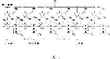
参照图4,图4为一个使用一串数字处理单元30所组成的可重新配置有限脉冲响应滤波器40的功能方块图。有限脉冲响应滤波器40包含一串对应数字处理单元30的加法器42,以及一个寄存器44,用来储存前述乘法器36形成2补码时所需累计的“1”的输出。加法器42由数字处理单元30接收对应的正负号和加数讯号,并输出一过滤后的数字讯号,其中每一加法器42处理一部份总数。一预先设计的控制讯号经由数字处理单元30的SIPO寄存器38被序列式的汇入滤波器40,多工器34会连结相邻的数字处理单元30,并根据其需要的CSD系数来设定乘法器36和移位器37。因此,CSD表示系数的大小及准确性,仅受到数字处理单元30组合数目的影响,这个结果使得有限脉冲响应滤波器40可被设定成用来处理一数字输入讯号。Referring to FIG. 4 , FIG. 4 is a functional block diagram of a reconfigurable finite
请参考图5,图5显示根据本发明的一个可重新配置的有限脉冲响应滤波器的处理组件50。处理组件50的结构近似有限脉冲响应滤波器40,但是处理组件50已被最佳化,以减少潜在因素并使IC制造更有效率。处理组件50包括一串数字处理单元30、一个组合的加法器52、一寄存器54以及一正负号延伸产生器56。因为数字处理单元30的输出与加法器52累计总和的精确度的差异,需要正负号延伸产生器56基于数字处理单元30的正负号输出,来产生正负号延伸位。寄存器54会储存Acc讯号(数字处理单元30中负数CSD的数目),以进行数字处理单元30中的乘法器36所需的2的补码运算。加法器52会加总数字处理单元30的加数输出、正负号延伸产生器56的输出以及寄存器54的累计总和,并且输出一个过滤后的数字讯号。处理组件50被以已知的流水线(pipeline)排列方法来加以组合,例如同时串接多个处理组件50。Please refer to FIG. 5 , which shows a
当加法器52的累计总和的位长度大于每一数字处理单元30的加数输出时,则需要使用正负号延伸产生器56。此外,为了省电,数字处理单元30的正负号延伸位需个别地操控,而不是将数字处理单元30的加数延伸至加法器52的位长度。正负号延伸产生器56会依据数字处理单元30的正负号讯号,并经由检查正负号讯号的非负数数目与对应正负号延伸位的总合之间的关系,来计算出正负号延伸位的总数。When the bit length of the cumulative sum of the
假设在处理组件50中的每一个数字处理单元30皆使用8位滤波系数来处理8位数据,以产生一个15位输出(如图3中的一个14位加数讯号以及一个1位正负号讯号),并假设滤波器输出如同Acc一样为24位宽度,则正负号延伸产生器56的输出为10位。正负号延伸产生器56包含一多工器,当有任何数字处理单元30的正负号讯号为1时,则其7个MSB输出为1111111,而当没有任何的正负号讯号为1时,则其输出是0000000。正负号延伸产生器56设定三个LSB的值,以使其等于正负数讯号中非负数的数目的二进制表示法的三个LSB。因此在这个例子中,一个10位正负号延伸讯号会由正负号延伸产生器56输出至加法器52。Assume that each
延续上述的例子,加法器52会加总八个数字处理单元30的八个14位加数讯号、寄存器54上的一个24位累计总和以及10位正负号延伸讯号。加法器52包含五个二层排列的14位全加器数组,用来将在寄存器54上的累计总和的14个LSB以及8个加数讯号,压缩成四个14位讯号。会有二层的保留进位(carry-save)加法器被用来加总寄存器54上的十个MSB、正负号延伸讯号以及上述四个14位讯号。加法器52还包括一ELM加法器,用来减少关键路径延迟并计算最后总和,如T.P.Kelliher、R.M.Owens、M.J.Irwin以及T.T.Hwang在“ELM-A Fast Addition Algorithm Discovered by a Program,”IEEE Transactions on Computers,vol.41,pp.1181-1184,Sept.1992,中所述。Continuing the above example, the
在图3及图5中可看到,无论为了表达一滤波系数而使用了多少个CSD或多少个数字处理单元,处理组件50的关键路径都只有包含一个系数乘法器(乘法器36和移位器37)以及一个加法器52。图4中的有限脉冲响应滤波器40也是一个实例,有限脉冲响应滤波器40是由以流水线方法排列的数个处理组件50所串联而成。故可确切地说,本发明的关键路径与滤波系数无关。As can be seen in FIGS. 3 and 5, no matter how many CSDs or how many digital processing units are used to express a filter coefficient, the critical path of the
在实际的应用上,本发明可用单多晶硅层四金属层(single polyquadruple-metal)0.35微米制程的CMOS来实行。依照上述使用八个数字处理单元30来处理8位讯号数据的例子,经量测结果显示所制造出来的芯片在2.5V供应电压及86MHz运作时钟下操作时,其消耗功率为16.5mW。In practical applications, the present invention can be implemented by CMOS with a single polyquadruple-metal 0.35 micron process. According to the above-mentioned example of using eight
相较于已知的有限脉冲响应滤波器,本发明的有限脉冲响应滤波器的数字处理单元具有一个包含一系数乘法器及一最佳化组合加法器的关键延迟路径,该关键延迟路径与系数准确性或位数目无关。此外,本发明的数字处理单元可被组合,用来处理在同样可重新配置的有限脉冲响应滤波器或处理单元中具有大范围准确性的系数,而且此种有限脉冲响应滤波器因具有可扩充性、模块性及可串接性可便于使用在VLSI设计中。Compared with known finite impulse response filters, the digital processing unit of the finite impulse response filter of the present invention has a critical delay path comprising a coefficient multiplier and an optimized combination adder, the critical delay path and the coefficient Accuracy or bit count is irrelevant. Furthermore, the digital processing units of the present invention can be combined to process coefficients with a wide range of accuracy in similarly reconfigurable finite impulse response filters or processing units, and such finite impulse response filters have scalable The flexibility, modularity and cascadeability can be easily used in VLSI design.
以上所述仅为本发明的较佳实施例,凡依本发明权利要求所做的均等变化与修饰,皆应属本发明专利的涵盖范围。The above descriptions are only preferred embodiments of the present invention, and all equivalent changes and modifications made according to the claims of the present invention shall fall within the scope of the patent of the present invention.
Claims (18)
Translated fromChineseApplications Claiming Priority (2)
| Application Number | Priority Date | Filing Date | Title |
|---|---|---|---|
| US10/248,920 | 2003-03-02 | ||
| US10/248,920US7277479B2 (en) | 2003-03-02 | 2003-03-02 | Reconfigurable fir filter |
Publications (2)
| Publication Number | Publication Date |
|---|---|
| CN1525642A CN1525642A (en) | 2004-09-01 |
| CN100336300Ctrue CN100336300C (en) | 2007-09-05 |
Family
ID=32907507
Family Applications (1)
| Application Number | Title | Priority Date | Filing Date |
|---|---|---|---|
| CNB031277306AExpired - Fee RelatedCN100336300C (en) | 2003-03-02 | 2003-08-08 | Reconfigurable Finite Impulse Response Filter |
Country Status (3)
| Country | Link |
|---|---|
| US (1) | US7277479B2 (en) |
| CN (1) | CN100336300C (en) |
| TW (1) | TWI263402B (en) |
Families Citing this family (20)
| Publication number | Priority date | Publication date | Assignee | Title |
|---|---|---|---|---|
| CN1306390C (en)* | 2000-10-16 | 2007-03-21 | 诺基亚公司 | Multiplier and shift device using signed digit representation |
| US7266255B1 (en)* | 2003-09-26 | 2007-09-04 | Sun Microsystems, Inc. | Distributed multi-sample convolution |
| EP1650869A1 (en)* | 2004-10-20 | 2006-04-26 | STMicroelectronics Pvt. Ltd | A device for implementing a sum of products expression |
| US7617267B1 (en)* | 2005-08-10 | 2009-11-10 | Nvidia Corporation | Configurable multi-tap filter |
| EP1879292B1 (en)* | 2006-07-10 | 2013-03-06 | Harman Becker Automotive Systems GmbH | Partitioned fast convolution |
| JPWO2008018197A1 (en)* | 2006-08-08 | 2009-12-24 | パナソニック株式会社 | Digital filter, synthesizing apparatus thereof, synthesizing program, and synthesizing program recording medium |
| TWI343021B (en)* | 2006-10-24 | 2011-06-01 | Princeton Technology Corp | Data transformation method and data transformation circuit capable of saving numeral operations |
| CN101072019B (en)* | 2007-04-19 | 2010-05-19 | 华为技术有限公司 | A filter and its filtering method |
| KR100947084B1 (en) | 2008-04-28 | 2010-03-10 | 엘아이지넥스원 주식회사 | Finite impulse response filter and signal processing method using the same |
| US8479133B2 (en)* | 2009-01-27 | 2013-07-02 | Xilinx, Inc. | Method of and circuit for implementing a filter in an integrated circuit |
| US8259786B2 (en)* | 2009-02-10 | 2012-09-04 | Redpine Signals, Inc. | Channel estimation filter for OFDM receiver |
| CN102510273B (en)* | 2011-12-27 | 2014-05-07 | 中国科学院自动化研究所 | Finite impulse response (FIR) filter |
| US9893714B2 (en) | 2015-09-01 | 2018-02-13 | Nxp Usa, Inc. | Configurable FIR filter with segmented cells |
| TWI575896B (en)* | 2015-12-03 | 2017-03-21 | 晨星半導體股份有限公司 | Signal Detection Method and Device |
| CN108429546B (en)* | 2018-03-06 | 2021-11-05 | 深圳大学 | A Design Method of Hybrid FIR Filter |
| CN108616265B (en)* | 2018-05-04 | 2022-07-01 | 重庆邮电大学 | Circuit structure of RNS DWT filter bank based on five-modulus residue number basis |
| US10581407B2 (en)* | 2018-05-08 | 2020-03-03 | The Boeing Company | Scalable fir filter |
| CN108832908A (en)* | 2018-05-23 | 2018-11-16 | 成都玖锦科技有限公司 | Multipath high-speed filter implementation method based on FPGA |
| US12093193B2 (en)* | 2019-11-06 | 2024-09-17 | Stmicroelectronics International N.V. | High throughput digital filter architecture for processing unary coded data |
| CN112564672B (en)* | 2020-11-18 | 2024-08-13 | 南京航空航天大学 | Reconfigurable architecture of low-complexity FIR filter based on secret bit information embedding system |
Citations (5)
| Publication number | Priority date | Publication date | Assignee | Title |
|---|---|---|---|---|
| US5031133A (en)* | 1989-02-16 | 1991-07-09 | Nec Corporation | FIR digital filter for high-speed communications systems |
| US5345426A (en)* | 1993-05-12 | 1994-09-06 | Hewlett-Packard Company | Delay interpolator for digital phased array ultrasound beamformers |
| US5479363A (en)* | 1993-04-30 | 1995-12-26 | The Regents Of The University Of California | Programmable digital signal processor using switchable unit-delays for optimal hardware allocation |
| CN1213217A (en)* | 1997-09-26 | 1999-04-07 | 朗迅科技公司 | Filter structure and method |
| CN1329301A (en)* | 2000-06-21 | 2002-01-02 | 智原科技股份有限公司 | Data processing device and method thereof |
Family Cites Families (9)
| Publication number | Priority date | Publication date | Assignee | Title |
|---|---|---|---|---|
| JPH0435213A (en)* | 1990-05-28 | 1992-02-06 | Hitachi Ltd | filter circuit |
| US5268877A (en)* | 1992-05-11 | 1993-12-07 | The United States Of America As Represented By The Secretary Of The Navy | Digital beamforming and filtering circuit |
| US5287299A (en)* | 1992-05-26 | 1994-02-15 | Monolith Technologies Corporation | Method and apparatus for implementing a digital filter employing coefficients expressed as sums of 2 to an integer power |
| KR100248021B1 (en)* | 1995-09-30 | 2000-03-15 | 윤종용 | Method and circuit of signal processing of csd filter |
| JP3204151B2 (en)* | 1997-02-13 | 2001-09-04 | 日本電気株式会社 | Adaptive filter |
| US6108681A (en)* | 1998-02-27 | 2000-08-22 | Philips Electronics North America Corporation | System for sharing resources in a digital filter |
| US6163788A (en)* | 1998-06-25 | 2000-12-19 | Industrial Technology Research Institute | Programmable finite impulse response processor with scalable dynamic data range |
| US6590931B1 (en)* | 1999-12-09 | 2003-07-08 | Koninklijke Philips Electronics N.V. | Reconfigurable FIR filter using CSD coefficient representation |
| US6633847B1 (en)* | 2000-01-05 | 2003-10-14 | Motorola, Inc. | Voice activated circuit and radio using same |
- 2003
- 2003-03-02USUS10/248,920patent/US7277479B2/ennot_activeExpired - Fee Related
- 2003-07-23TWTW092120150Apatent/TWI263402B/ennot_activeIP Right Cessation
- 2003-08-08CNCNB031277306Apatent/CN100336300C/ennot_activeExpired - Fee Related
Patent Citations (5)
| Publication number | Priority date | Publication date | Assignee | Title |
|---|---|---|---|---|
| US5031133A (en)* | 1989-02-16 | 1991-07-09 | Nec Corporation | FIR digital filter for high-speed communications systems |
| US5479363A (en)* | 1993-04-30 | 1995-12-26 | The Regents Of The University Of California | Programmable digital signal processor using switchable unit-delays for optimal hardware allocation |
| US5345426A (en)* | 1993-05-12 | 1994-09-06 | Hewlett-Packard Company | Delay interpolator for digital phased array ultrasound beamformers |
| CN1213217A (en)* | 1997-09-26 | 1999-04-07 | 朗迅科技公司 | Filter structure and method |
| CN1329301A (en)* | 2000-06-21 | 2002-01-02 | 智原科技股份有限公司 | Data processing device and method thereof |
Also Published As
| Publication number | Publication date |
|---|---|
| US20040170223A1 (en) | 2004-09-02 |
| TWI263402B (en) | 2006-10-01 |
| CN1525642A (en) | 2004-09-01 |
| TW200418264A (en) | 2004-09-16 |
| US7277479B2 (en) | 2007-10-02 |
Similar Documents
| Publication | Publication Date | Title |
|---|---|---|
| CN100336300C (en) | Reconfigurable Finite Impulse Response Filter | |
| TWI783295B (en) | Multiplier and multiplication method | |
| CN1503938A (en) | Multiplication logic circuit | |
| CN1570848A (en) | Montgomery modular multiplier and method thereof using carry save addition | |
| CN1781076A (en) | Multiplier Architecture Combining Polynomial and Natural Multiplication | |
| CN1244242C (en) | Digital filter for mobile communication system and method of operation thereof | |
| Balaji et al. | Design of fir filter with fast adders and fast multipliers using rns algorithm | |
| CN1419388A (en) | Low power filter structure using vertical public subexpression and design method thereof | |
| CN100435088C (en) | Optimized coefficient multiplier for standard signed numbers | |
| CN1099071C (en) | Digital filter device having bit shifter unit | |
| JPH09325955A (en) | Square root arithmetic circuit for sum of squares | |
| CN1771665A (en) | Bi-quad digital filter configured with a bit binary rate multiplier | |
| CN1708902A (en) | Method for determining filter coefficients of digital filter and digital filter | |
| CN101178643A (en) | Data conversion method and data conversion circuit capable of saving digital operations | |
| CN108616265B (en) | Circuit structure of RNS DWT filter bank based on five-modulus residue number basis | |
| CN1567178A (en) | Multiplier restructuring algorithm and circuit thereof | |
| Meher et al. | Reconfigurable FIR filter for dynamic variation of filter order and filter coefficients | |
| Chen et al. | Design and implementation of a reconfigurable FIR filter | |
| Raj et al. | A paradigm of distributed arithmetic (DA) approaches for digital FIR filter | |
| Hariprasad et al. | Image Processing Acceleration Using Radix-8 Booth Multiplier with Custom Designed 4: 2 Compressors | |
| Varalakshmi et al. | Implementation of Multiplier Architecture Using Efficientcarry Select Adders for Synthesizing Fir Filters | |
| Teja et al. | Implementation of vedic multiplier using modified architecture by routing rearrangement for high-optimization | |
| Xu et al. | Low power design for FIR filter | |
| CN113220267B (en) | A Multiplier Based on Booth Coding Bit Expansion and Its Implementation | |
| US7849118B2 (en) | Data transformation method and data transformation circuit capable of saving numeral operations |
Legal Events
| Date | Code | Title | Description |
|---|---|---|---|
| C06 | Publication | ||
| PB01 | Publication | ||
| C10 | Entry into substantive examination | ||
| SE01 | Entry into force of request for substantive examination | ||
| C14 | Grant of patent or utility model | ||
| GR01 | Patent grant | ||
| ASS | Succession or assignment of patent right | Owner name:MEDIATEK INC.; WANG ZHONGGUANG Free format text:FORMER OWNER: MEDIATEK INC. Effective date:20070914 | |
| C41 | Transfer of patent application or patent right or utility model | ||
| TR01 | Transfer of patent right | Effective date of registration:20070914 Address after:Hsinchu Science Industrial Park, Hsinchu, Taiwan Co-patentee after:Wang Zhongguang Patentee after:MediaTek.Inc Address before:Hsinchu Science Industrial Park, Hsinchu, Taiwan Patentee before:MediaTek.Inc | |
| CF01 | Termination of patent right due to non-payment of annual fee | ||
| CF01 | Termination of patent right due to non-payment of annual fee | Granted publication date:20070905 Termination date:20190808 |